

Page 1

SERVICE MANUAL
FILE NO.
Color Digital Camera
Contents
1. OUTLINE OF CIRCUIT DESCRIPTION .................... 2
2. DISASSEMBLY ........................................................ 11
3. ELECTRICAL ADJUSTMENT .................................. 14
4. USB STORAGE INFORMATION
REGISTRATION ...................................................... 19
5. TROUBLESHOOTING GUIDE................................. 20
6. PARTS LIST............................................................. 21
CABINET AND CHASSIS PARTS 1 ........................ 21
CABINET AND CHASSIS PARTS 2 ........................ 22
ELECTRICAL PARTS .............................................. 23
ACCESSORIES AND PACKING MATERIALS ........ 29
CIRCUIT DIAGRAMS &
PARTS POSITION FIGURE ....................................... C1
VPC-AZ1EX
(Product Code : 126 299 01)
(Europe)
(PAL General)
VPC-AZ1E
(Product Code : 126 299 02)
(U.K.)
VPC-AZ1
(Product Code : 126 299 03)
(U.S.A.)
(Canada)
PRODUCT SAFETY NOTICE
The components designated by a symbol ( ! ) in this schematic diagram designates components whose value are of
special significance to product safety. Should any component designated by a symbol need to be replaced, use only the part
designated in the Parts List. Do not deviate from the resistance, wattage, and voltage ratings shown.
CAUTION : Danger of explosion if battery is incorrectly replaced.
Replace only with the same or equivalent type recommended by the manufacturer.
Discard used batteries according to the manufacturer’s instructions.
NOTE : 1. Parts order must contain model number, part number, and description.
2. Substitute parts may be supplied as the service parts.
3. N. S. P. : Not available as service parts.
Design and specification are subject to change without notice.
SX511/EX, E, U
REFERENCE No. SM5310328
Page 2
1. OUTLINE OF CIRCUIT DESCRIPTION
1-1. CA1 and A PART OF CA2 CIRCUIT
DESCRIPTIONS
Around CCD block
1. IC Configuration
CA1 board
IC903 (ICX411AK) CCD imager
IC901 (CXD3400N) V driver
CA2 board
IC911 (H driver, CDS, AGC and A/D converter)
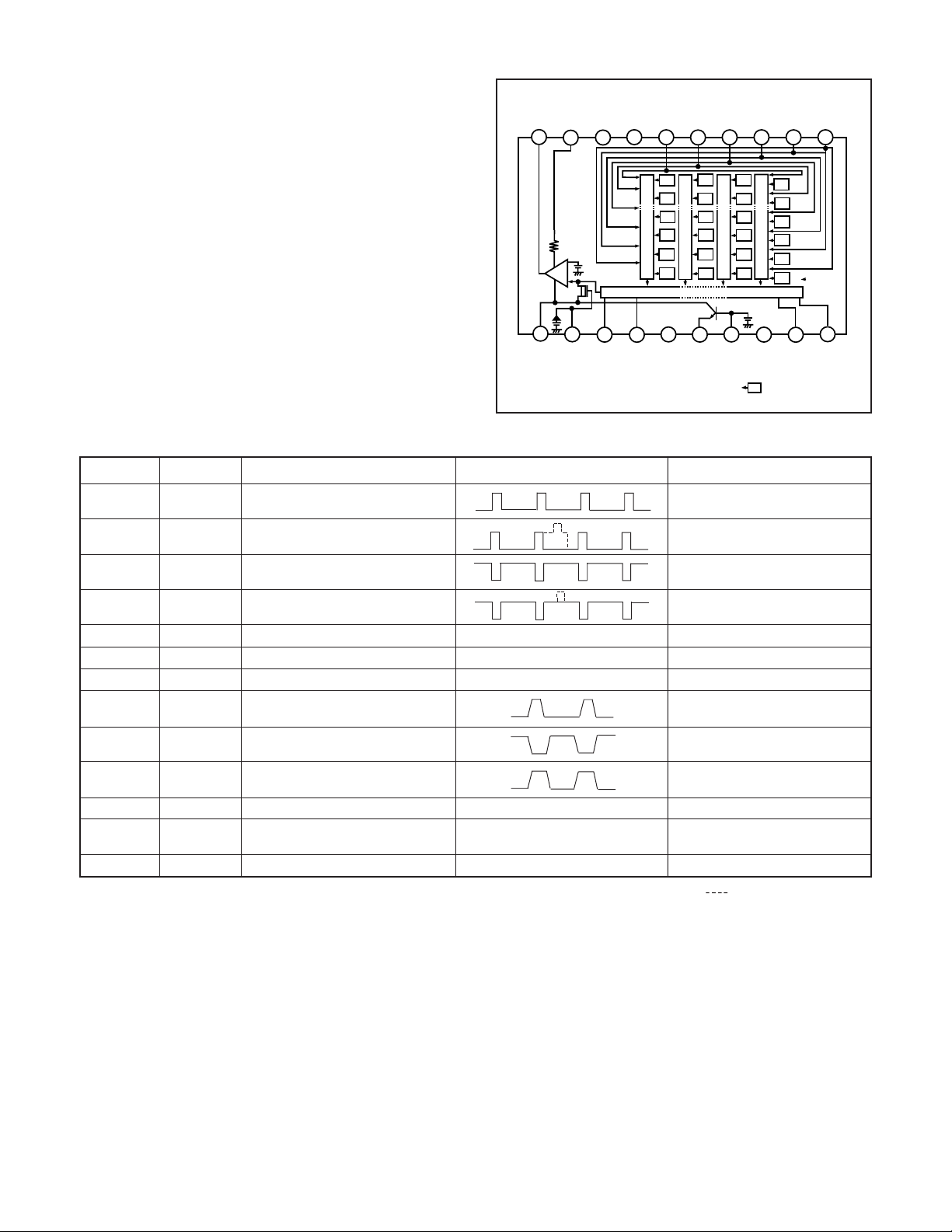
2. IC903 (CCD imager)
[Structure]
Interline type CCD image sensor
Image size Diagonal 8.293 mm (1/1.8 type)
Pixels in total 2384 (H) x 1734 (V)
Recording pixels 2288 (H) x 1712 (V)
10
11
1B
OUT
V
DD
V
9
12
GND
RG
Ø
TEST
8
13
2
Ø
H
Ø
V
TEST
7
6
Ye
G
Ye
G
Ye
Vertical register
G
Horizontal register
15
14
1
Ø
GND
H
Fig. 1-2. CCD Block Diagram
1A
Ø
Ø
V
V
4
5
Cy
Ye
Mg
G
Cy
Ye
Mg
G
Cy
Ye
Mg
G
17
16
SUB
SUB
C
Ø
(Note) : Photo sensor
3
18
Ø
V
L
V
Cy
Mg
Cy
Mg
Cy
Mg
19
2
3A
Ø
V
1
Ø
H
3B
2
1
(Note)
20
4
Ø
V
2
Ø
H
Pin No.
1
2, 3
4
5, 6
9, 15
10
11
12
13, 20
14, 19
16
17
18
Symbol
4
Vø
Vø
3A, Vø3B
Vø2
Vø1A, Vø1B
GND
OUT
V
VDD
øRG
Hø2
Hø
1
øSUB
CSUB
VL
Pin Description
Vertical register transfer clock
Vertical register transfer clock
Vertical register transfer clock
Vertical register transfer clock
GND
Signal output
Circuit power
Reset gate clock
Horizontal register transfer clock
Horizontal register transfer clock
Substrate clock
Substrate bias
Protection transistor bias
Table 1-1. CCD Pin Description
Waveform
GND
DC
DC
DC
DC
Voltage
-7.5 V, 0 V
-7.5 V, 0 V, 15 V
-7.5 V, 0 V
-7.5 V, 0 V, 15 V
0 V
Aprox. 10 V
15 V
12.5 V, 16 V
0 V, 5 V
0 V, 5 V
Approx. 8 V
Approx. 8 V
(Different from every CCD)
When sensor read-out
– 2 –
Page 3
3. IC901 (V Driver) and IC911 (H Driver)
An H driver and V driver are necessary in order to generate
the clocks (vertical transfer clock, horizontal transfer clock
and electronic shutter clock) which driver the CCD.
IC901 is V driver. In addition the XV1-XV4 signals which are
output from IC102 are the vertical transfer clocks, and the
XSG signal which is output from IC102 is superimposed onto
XV1 and XV3 at IC901 in order to generate a ternary pulse.
In addition, the XSUB signal which is output from IC102 is
used as the sweep pulse for the electronic shutter. A H driver
is inside IC911, and H1, H2 and RG clock are generated at
IC911.
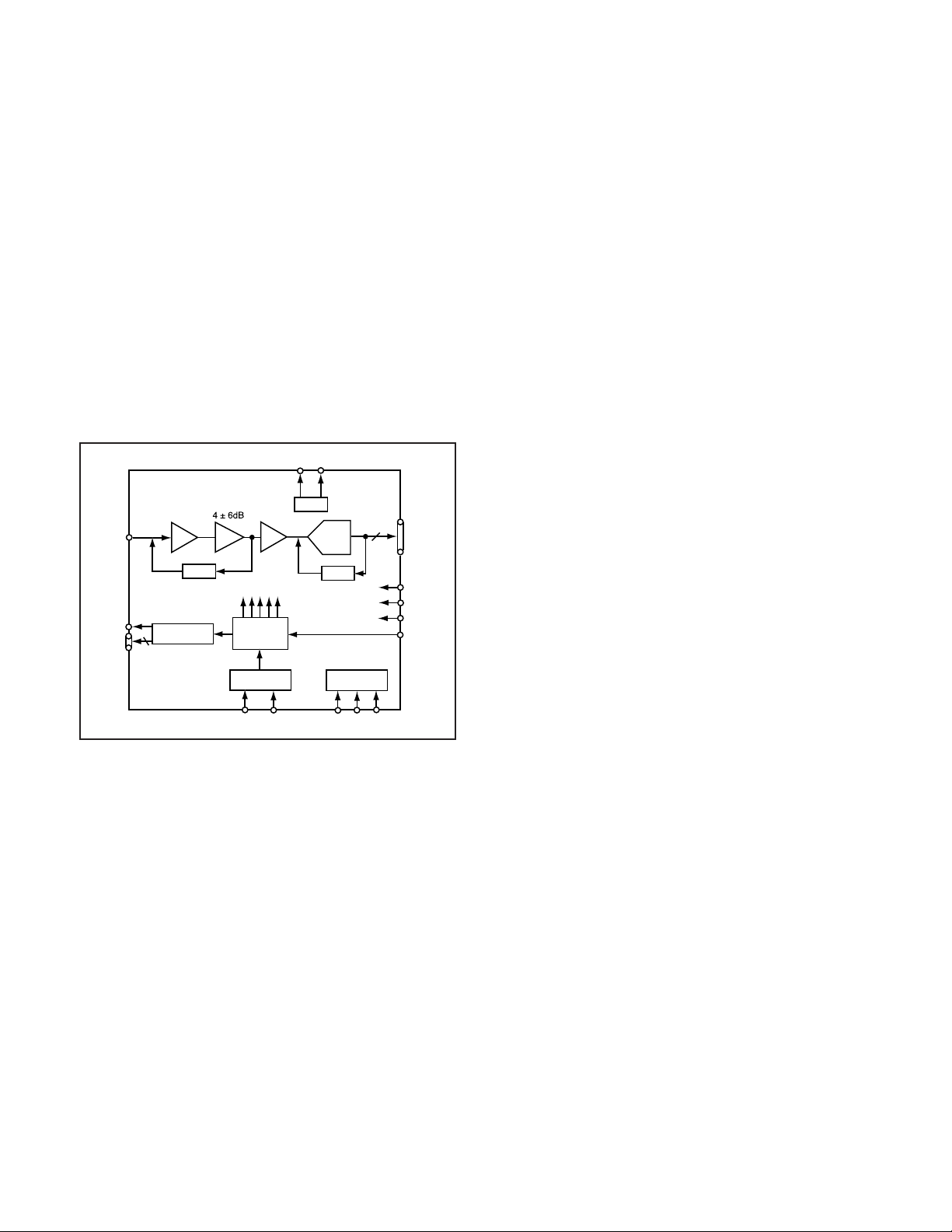
4. IC911 (CDS, AGC Circuit and A/D Converter)
The video signal which is output from the CCD is input to Pin
(29) of IC911. There are inside the sampling hold block, AGC
block and A/D converter block.
The setting of sampling phase and AGC amplifier is carried
out by serial data at Pin (37) of IC911. The video signal is
carried out A/D converter, and is output by 12-bit.
VRB
VRT
VREF
CCDIN
CDS
PxGA
2~36 dB
VGA
ADC
12
DOUT
5. Lens drive block
5-1. Iris and shutter drive
The shutter and iris stepping motor drive signals (IIN1, IIN2,
IIN3 and IIN4) which are output from the ASIC (IC102) are
used to drive by the motor driver (IC951), and are then used to
drive the iris steps.
5-2. Focus drive
The focus stepping motor drive signals (FIN1, FIN2, FIN3 and
FIN4) which are output from the ASIC expansion port (IC107)
are used to drive by the motor driver (IC952). Detection of the
standard focusing positions is carried out by means of the
photointerruptor (PI) inside the lens block.
5-3. Zoom drive
The zoom stepping motor drive signals (ZIN1, ZIN2, ZIN3 and
ZIN4) which are output from the ASIC expansion port (IC107)
are used to drive by the motor driver (IC952). Detection of the
standard zoom positions is carried out by means of
photoreflector (ZPI) inside the lens block.
RG
H1-H4
HORIZONTAL
4
DRIVERS
CLAMP
INTERNAL
CLOCKS
PRECISION
TIMING
CORE
SYNC
GENERATOR
VD
HD
Fig. 1-2. IC911 Block Diagram
CLAMP
INTERNAL
REGISTERS
SL
SCK
CLPOB
CLPDM
PBLK
CLI
SDATA
– 3 –
Page 4

1-2. CA2 CIRCUIT DESCRIPTION
1. Circuit Description
1-1. Digital clamp
The optical black section of the CCD extracts averaged values from the subsequent data to make the black level of the
CCD output data uniform for each line. The optical black section of the CCD averaged value for each line is taken as the
sum of the value for the previous line multiplied by the coefficient k and the value for the current line multiplied by the
coefficient 1-k.
1-2. Signal processor
1. γ correction circuit
This circuit performs (gamma) correction in order to maintain
a linear relationship between the light input to the camera
and the light output from the picture screen.
2. Color generation circuit
This circuit converts the CCD data into RGB signals.
3. Matrix circuit
This circuit generates the Y signals, R-Y signals and B-Y signals from the RGB signals.
4. Horizontal and vertical aperture circuit
This circuit is used gemerate the aperture signal.
1-3. AE/AWB and AF computing circuit
The AE/AWB carries out computation based on a 64-segment
screen, and the AF carries out computations based on a 6segment screen.
1-4. SDRAM controller
This circuit outputs address, RAS, CAS and AS data for controlling the SDRAM. It also refreshes the SDRAM.
1-5. Communication control
1. SIO
This is the interface for the 8-bit microprocessor.
2. PIO/PWM/SIO for LCD
8-bit parallel input and output makes it possible to switch between individual input/output and PWM input/output.
1-6. TG/SG
Timing generated for 4 million pixel CCD control.
1-7. Digital encorder
It generates chroma signal from color difference signal.
2. Outline of Operation
When the shutter opens, the reset signals (ASIC and CPU)
and the serial signals (“take a picture” commands) from the
8-bit microprocessor are input and operation starts.
When the TG/SG drives the CCD, picture data passes through
the A/D and CDS, and is then input to the ASIC as 12-bit
data. The AF, AE, AWB, shutter, and AGC value are computed from this data, and three exposures are made to obtain
the optimum picture. The data which has already been stored
in the SDRAM is read by the CPU and color generation is
carried out. Each pixel is interpolated from the surrounding
data as being either Ye, Cy, Mg or B primary color data to
produce R, G and B data. At this time, correction of the lens
distortion which is a characteristic of wide-angle lenses is
carried out. After AWB and γ processing are carried out, a
matrix is generated and aperture correction is carried out for
the Y signal, and the data is then compressed by JPEG and
is then written to card memory (smart media).
When the data is to be output to an external device, it is taken
data from the memory and output via the USART. When played
back on the LCD and monitor, data is transferred from memery
to the SDRAM, and the image is then elongated so that it is
displayed over the SDRAM display area.
3. LCD Block
During monitoring, YUV conversion is carried out for the 12bit CCD data which is input from the A/D conversion block to
the ASIC and is then transferred to the DRAM so that the
CCD data can be displayed on the LCD.
The data which has accumulated in the DRAM is passed
through the NTSC encoder , and after D/A conversion is carried out to change the data into a Y/C signal, the data is sent
to the LCD panel and displayed.
If the shutter button is pressed in this condition, the 12-bit
data which is output from the A/D conversion block of the
CCD is sent to the DRAM (DMA transfer), and after processor, it is displayed on the LCD as a freeze-frame image.
During playback, the JPEG image data which has accumulated in the flash memory is converted to YUV signals, and
then in the same way as during monitoring, it is passed through
the NTSC endoder, and after D/A conversion is carried out to
change the data into a Y/C signal, the data is sent to the LCD
panel and displayed.
The two analog signal (Y/C signals) from the ASIC are converted into RGB signals by the LCD driver, and these RGB
signals and the control signal which is output by the LCD driver
are used to drive the LCD panel. The RGB signals are 1H
transposed so that no DC component is present in the LCD
element, and the two horizontal shift register clocks drive the
horizontal shift registers inside the LCD panel so that the 1H
transposed RGB signals are applied to the LCD panel. Because the LCD closes more as the difference in potential between the COM (common polar voltage: fixed at DC) and the
R, G and B signals becomes greater, the display becomes
darker; if the difference in potential is smaller, the element
opens and the LCD become brighter.
– 4 –
Page 5

1-3. CA3 CIRCUIT DESCRIPTION
1. Outline
This is the main CA3 power block, and is comprised of the
following blocks.
Switching controller (IC511)
Lens system 3.4 V power output (L5106, Q5104, D5105,
C5117)
Backlight power output (L5102, Q5101, C5113)
LCD system power output (Q5107, T5101)
2. Switching Controller (IC511)
This is the basic circuit which is necessary for controlling the
power supply for a PWM-type switching regulator, and is provided with six built-in channels. They are CH5 (lens system
3.4 V), CH4 (backlight) and CH3 (LCD system). CH1, CH2
and CH6 are not used. Feedback from 3.4 V (D) C (CH5) and
+12.4 V (L) power supply output are received, and the PWM
duty is varied so that each one is maintained at the correct
voltage setting level. CH4 is feedback from 10 mA power supply output are received, and the PWM duty is varied so that
each one is maintained at the correct voltage setting level.
2-1. Short-circuit protection circuit
If output is short-circuited for the length of time determined
by the condenser which is connected to Pin (18) of IC511, all
output is turned off. The control signal (P(A) ON, LCD ON
and BL ON) are recontrolled to restore output.
3. Lens system 3.4 V Power Output
3.4 V (D) C is output for lens. Feedback for the 3.4 V (D) is
provided to the swiching controller (Pin (8) of IC511) so that
PWM control can be carried out.
4. Backlight Power Output
10 mA (L) is output. The backlighting turns on when current
flows in the direction from pin (1) to pin (2) of CN531. At this
time, a feedback signal is sent from pin (2) of CN531 to pin
(12) of IC511 through R5122 so that PWM control is carried
out to keep the current at a constant level (10 mA).
5. LCD System Power Output
12.4 V (L), 15 V (L) and 4 V (L) are output. Feedback for the
12.4 V (L) is provided to the switching controller (Pin (28) of
IC511) so that PWM control can be carried out.
– 5 –
Page 6

1-4. PW1 POWER CIRCUIT DESCRIPTION
1. Outline
This is the main power circuit, and is comprised of the following blocks.
Switching controller (IC501)
5.6 V system power output (L5001, Q5001)
5 V system power output (IC502)
Analog system power output (T5001, Q5002)
Digital 3.4 V system power output (L5005, Q5010)
Digital 1.8 V system power output (L5007, Q5014)
2. Switching Controller
This is the basic circuit which is necessary for controlling the
power supply for a PWM-type switching regulator, and is provided with six built-in channels, only CH3 (analog system),
CH2 (digital 1.8 V), CH5 (digital 3.4 V) and CH6 (5.6 V system) are used. CH1 and CH4 are not used. Feedback from
15.2 V (A) (CH1), 1.8 V (D) (CH2), 3.4 V (D) (CH5) and 5.6 V
(CH6) power supply outputs are received, and the PWM duty
is varied so that each one is maintained at the correct voltage
setting level.
2-1. Short-circuit Protection
If output is short-circuited for the length of time determined
by the condenser which is connected to Pin (18) of IC501, all
output is turned off. The control signal (P ON) are recontrolled
to restore output.
3. Analog System Power Output
15.2 V (A) and -7.7 V (A) are output. Feedback for the 15.2 V
(A) is provided to the switching controller (Pin (28) of IC501)
so that PWM control can be carried out.
4. Digital 1.8 V Power Output
1.8 V (D) is output. Feedback for the 1.8 V (D) is provided to
the switching controller (Pins (31) of IC501) so that PWM
control can be carried out.
5. Digital 3.4 V Power Output
3.4 V (D) is output. Feedback for the 3.4 V (D) is provided to
the swiching controller (Pin (8) of IC501) so that PWM control
can be carried out.
6. 5.6 V System Power Output
5.6 V is output. Feedback is provided to the swiching controller (Pin (4) of IC501) so that PWM control can be carried out.
– 6 –
Page 7

1-5. PW1 STROBE CIRCUIT DESCRIPTION
1. Charging Circuit
When UNREG power is supplied to the charge circuit and the
CHG signal becomes High (3.3 V), the charging circuit starts
operating and the main electorolytic capacitor is charged with
high-voltage direct current.
However, when the CHG signal is Low (0 V), the charging
circuit does not operate.
1-1. Power switch
When the CHG signal switches to Hi, Q5406 turns ON and
the charging circuit starts operating.
1-2. Power supply filter
L5401 and C5401 constitute the power supply filter. They
smooth out ripples in the current which accompany the switching of the oscillation transformer.
1-3. Oscillation circuit
This circuit generates an AC voltage (pulse) in order to increase the UNREG power supply voltage when drops in current occur. This circuit generates a drive pulse with a frequency
of approximately 50-100 kHz. Because self-excited light omission is used, the oscillation frequency changes according to
the drive conditions.
2. Light Emission Circuit
When RDY and TRIG signals are input from the ASIC expansion port, the stroboscope emits light.
2-1. Emission control circuit
When the RDY signal is input to the emission control circuit,
Q5409 switches on and preparation is made to let current
flow to the light emitting element. Moreover, when a STOP
signal is input, the stroboscope stops emitting light.
2-2. Trigger circuit
When a TRIG signal is input to the trigger circuit, D5405
switches on, a high-voltage pulse of several kilovolts is generated inside the trigger circuit, and this pulse is then applied
to the light emitting part.
2-3. Light emitting element
When the high-voltage pulse form the trigger circuit is applied to the light emitting part, currnet flows to the light emitting element and light is emitted.
Beware of electric shocks.
1-4. Oscillation transformer
The low-voltage alternating current which is generated by the
oscillation control circuit is converted to a high-voltage alternating current by the oscillation transformer.
1-5. Rectifier circuit
The high-voltage alternating current which is generated at
the secondary side of T5401 is rectified to produce a highvoltage direct current and is accumulated at electrolytic capacitor C5144 on the CA3 board.
1-6. Voltage monitoring circuit
This circuit is used to maintain the voltage accumulated at
C5144 at a constance level.
After the charging voltage is divided and converted to a lower
voltage by R5417 and R5419, it is output to the SY1 circuit
board as the monitoring voltage VMONIT. When this VMONIT
voltage reaches a specified level at the SY1 circuit board, the
CHG signal is switched to Low and charging is interrupted.
– 7 –
Page 8

1-6. SY1 CIRCUIT DESCRIPTION
1. Configuration and Functions
For the overall configuration of the SY1 circuit board, refer to the block diagram. The SY1 circuit board centers around a 8-bit
microprocessor (IC301), and controls camera system condition (mode).
The 8-bit microprocessor handles the following functions.
1. Operation key input, 2. Clock control and backup, 3. Power ON/OFF, 4. Storobe charge control, 5. Signal input and output for
zoom and lens control.
Pin
1~4
5
6
7
8
9
10
11
12
13
14
15
16
17
18
19
20
21
22
23
24 VDD
25 AVSS
26~29 SCAN IN 3~0
30
31 DC_IN
32
33
34
35
36
37
38
39
40
41
42
43
44
45
46
47
48
STBY_LED (GREEN)
Signal
SCAN OUT 0~3
P ON
PA ON
LCD ON
BL ON
VSS
VDD
SELF_LED
STBY_LED (RED)
AVREF_ON
SI
SO
SCK
PRG SI
PRG SO
PRG SCK
AV J ACK
NOT USED
CHG ON
NOT USED
CHG VOL
BATTERY
AVREF
AVDD
RESET
XCOUT
XCIN
IC
XOUT
XIN
VSS
BAT OFF
SREQ
JOG 0
SCAN_IN5
JOG 1
RSENS 1
I/O
O
O
O
O
O
O
O
O
O
O
I/O
O
I/O
O
O
O
Outline
Key matrix output
Digital power ON/OFF control H : ON
Analog power ON/OFF control H : ON
LCD power ON/OFF control H : ON
LCD backlight power ON/OFF H : ON
-
-
I
I
I
-
-
-
I
-
I
I
I
-
-
I
I
I
I
-
I
I
I
I
I
I
GND
VDD
Self-timer LED control L : ON
Stand-by LED (green) control L : ON
Stand-by LED (red) control L : ON
A/D converter standard voltage control L : ON
Receiving data (from ASIC)
Sending data (to ASIC)
Communication clock (to ASIC)
Flash memory write receiving data
Flash memory write sending data
Flash memory write communication clock
AV jack connection detection H : AV JACK detection
-
Flash charge control H : ON
VDD
Analog GND
Key scan input
-
DC JACK/battery detection input (analog input)
Storobe charge voltage detection (analog input)
Battery voltage detection (analog input)
Analog standard voltage input terminal
A/D converter analog power terminal
Reset input
Clock oscillation terminal (32.768 kHz)
Clock oscillation terminal
Flash memory writing voltage
Main clock oscillation terminal (4MHz)
Main clock oscillation terminal
GND
Battery OFF detection
Serial communication requirement (from ASIC)
Jog shuttle input 0
Key scan input 5
Jog shuttle input 1
Inclination sensor input 1 L : Inclination detection (left)
See next page →
– 8 –
Page 9
49 BR OPEN
50
51
52
53
54
55
56
57
58
59
60
61
62
63
64
RSENS 0
CARD
BUZZER
SCAN IN 4
SCAN OUT 4
WAKE UP
SYMUTE
USB
NOT USED
NOT USED -
BR CLOSE
NOT USED
ASIC TEST O ASIC reset control signal 1 L : Reset
ASIC RESET
MAIN RESET
O
I Inclination sensor input 0 L : Inclination detection (right)
I
O
I
O
I
O
I
--
O
-
O
O
Table 4-1. 8-bit Microprocessor Port Specification
Barrier open control H : Open
CF card insertion detection L : Insertion
Buzzer beep tone output L : Pulse output
Key scan input 4
Key scan output 4
-
Audio mute control L : Mute
USB connector detection L : USB detecion
-
Barrier close control L : Close
-
ASIC reset control signal 2 L : Reset
Main CPU reset singal L : Reset
2. Internal Communication Bus
The SY1 circuit board carries out overall control of camera operation by detecting the input from the keyboard and the condition
of the camera circuits. The 8-bit microprocessor reads the signals from each sensor element as input data and outputs this data
to the camera circuits (ASIC) or to the LCD display device as operation mode setting data. Fig. 4-1 shows the internal communication between the 8-bit microprocessor, ASIC and SPARC lite circuits.
MAIN RESET
S. REQ
8-bit
Microprocessor
Fig. 4-1 Internal Bus Communication System
ASIC SO
ASIC SI
ASIC SCK
ASIC TEST
ASIC RESET
3. Key Operation
For details of the key operation, refer to the instruction manual.
SCAN
SCAN
OUT
IN
0
1
2
3
4
0
← LEFT
TELE
MODE
STILL IMAGE
--
123
↑ UP
WIDE
SET FLASH MODE BARRIER OPEN
SEQUENTIAL
SHOT
→ RIGHT
PLAY MODE
INFO
VIDEO CLIP
SHOOTING
-
↓ DOWN
REC MODE
(LCD OFF)
SET UP
-
4
1st shutter
REC MODE
(LCD ON)
PC MODE
-
CPU
5
2nd shutter
-
BARRIER
CLOSE
TEST
POWER ON
Table 4-2. Key Operation
– 9 –
Page 10
4. Power Supply Control
The 8-bit microprocessor controls the power supply for the overall system.
The following is a description of how the power supply is turned on and off. When the battery is attached, a regulated 3.2 V
voltage is normally input to the 8-bit microprocessor (IC301) by IC302, so that clock counting and key scanning is carried out
even when the power switch is turned off, so that the camera can start up again. When the battery is removed, the 8-bit microprocessor operates in sleep mode using the backup capacitor. At this time, the 8-bit microprocessor only carries out clock
counting, and waits in standby for the battery to be attached again. When a switch is operated, the 8-bit microprocessor supplies
power to the system as required.
The 8-bit microprocessor first sets both the P (A) ON signal at pin (6) and the P ON signal at pin (5) to high, and then turns on the
DC/DC converter. After this, low signals are output from pins (62), (63) and (64) so that the ASIC is set to the active condition. If
the LCD monitor is on, the LCD ON signal at pin (7) set to high, and the DC/DC converter for the LCD monitor is turned on. Once
it is completed, the ASIC returns to the reset condition, all DC/DC converters are turned off and the power supply to the whole
system is halted.
ASIC,
memory
Power voltage
Power OFF
Power switch ON-
Auto power OFF
Shutter switch ON
CAMERA
Monitor OFF
LCD finder
Play back
Table 4-3. Camera Mode (Battery Operation)
Note) 4 MHz = Main clock operation, 32 kHz = Sub clock operation
3.3 V
OFF
OFF
ON
OFF
ON
ON
CCD
5 V (A)
+12 V etc.
OFF
OFF
ON→OFF
OFF
ON
OFF
8 bit
CPU
3.2 V
(ALWAYS)
32KHz OFF
4 MHz OFF
4 MHz OFF
4 MHz OFF
4 MHz ON
4 MHz ON
MONITOR
+12V etc.
LCD
5V (L)
– 10 –
Page 11
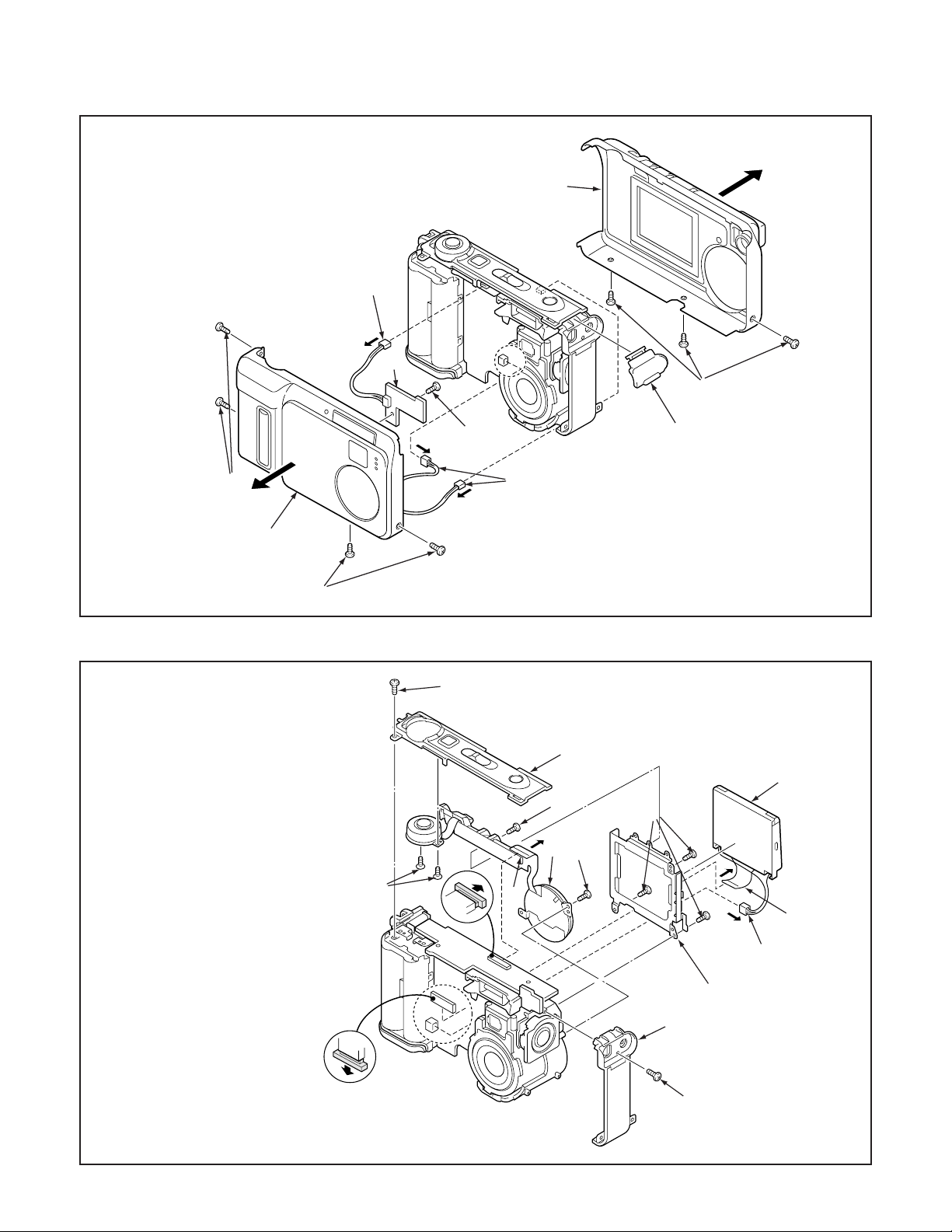
2. DISASSEMBLY
2-1. REMOVAL OF CABINET BACK, CABINET FRONT AND SY2 BOARD
1. Seven screws 1.7 x 4
2. Cabinet back
3. Cabinet front
4. Three connectors
5. Screw 1.7 x 5
6. SY2 board
7. Cover jack
4
6
2
1
1
3
1
2-2. REMOVAL OF CABINET TOP AND LCD
1. Screw 1.7 x 4
2. Cabinet left
3. Screw 1.7 x 2.5
4. Two screws 1.7 x 2.5
5. Cabinet top
6. Screw 1.7 x 3.5
7. Screw 1.7 x 4
8. FPC
9. Unit control panel
10. Connector
11. FPC
12. LCD
13. Three screws 1.7 x 4
14. Holder monitor
4
5
7
4
3
5
12
6
9
7
8
13
11
10
14
2
– 11 –
1
Page 12
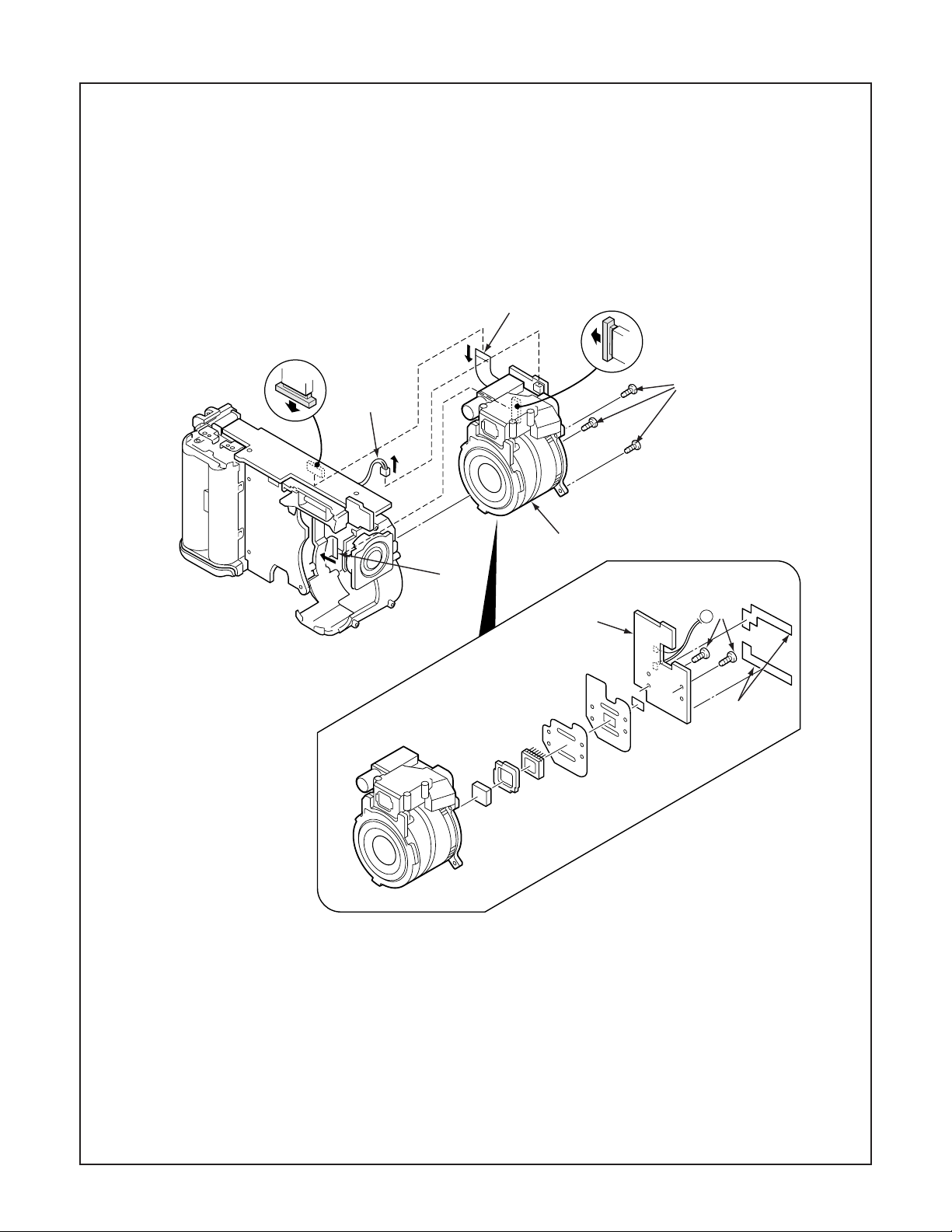
2-3. REMOVAL OF LENS ASSEMBLY AND CA1 BOARD
1
2
4
1. Connector
2. FPC
3. FPC
4. Three screws 1.7 x 4
5. Lens assembly
6. Two screws 1.7 x 5
7. Sheild tape CA1 lens
8. CA1 board
5
3
6
8
E
7
– 12 –
Page 13
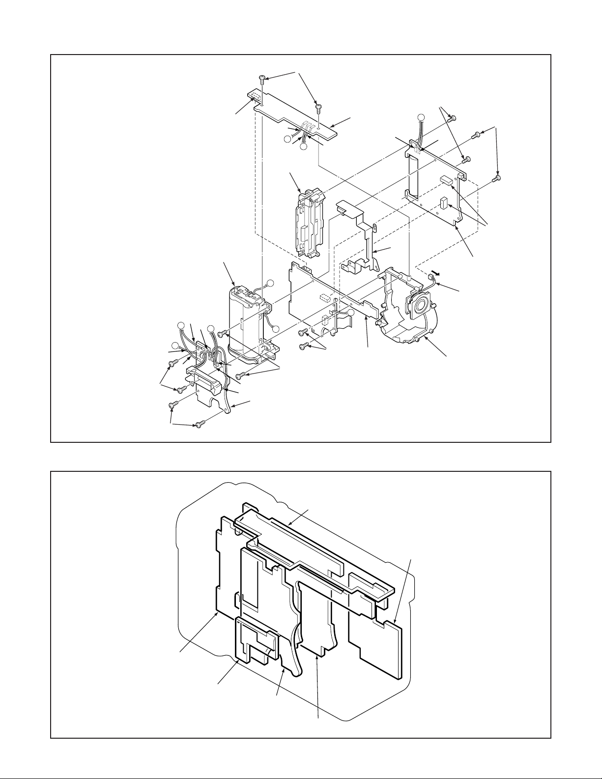
2-4. REMOVAL OF SY1 BOARD, PW1 BOARD, CA3 BOARD AND CA2 BOARD
1
1. Two screws 1.7 x 4
2. Connector
3. SY1 board
4. Four screws 1.7 x 4
5. PW1 board
6. Two screws 1.7 x 3.5
7. Two screws 1.7 x 4
8. Two screws 1.7 x 3.5
9. Holder battery
10. Two connectors
11. Holder card
12. Connector
13. CA3 board
14. Two screws 1.7 x 4
15. CA2 board
16. Holder lens
17. Holder chassis
C
B
red
gray
4
pink
red
2
black
A
white
D
11
9
A
D
blue
white
black
B
6
5
blue
14
3
gray
17
E
15
7
C
pink
8
10
13
12
16
2-5. BOARD LOCATION
4
SY1 board
CA1 board
CA2 board
SY2 board
PW1 board
CA3 board
– 13 –
Page 14
3. ELECTRICAL ADJUSTMENT
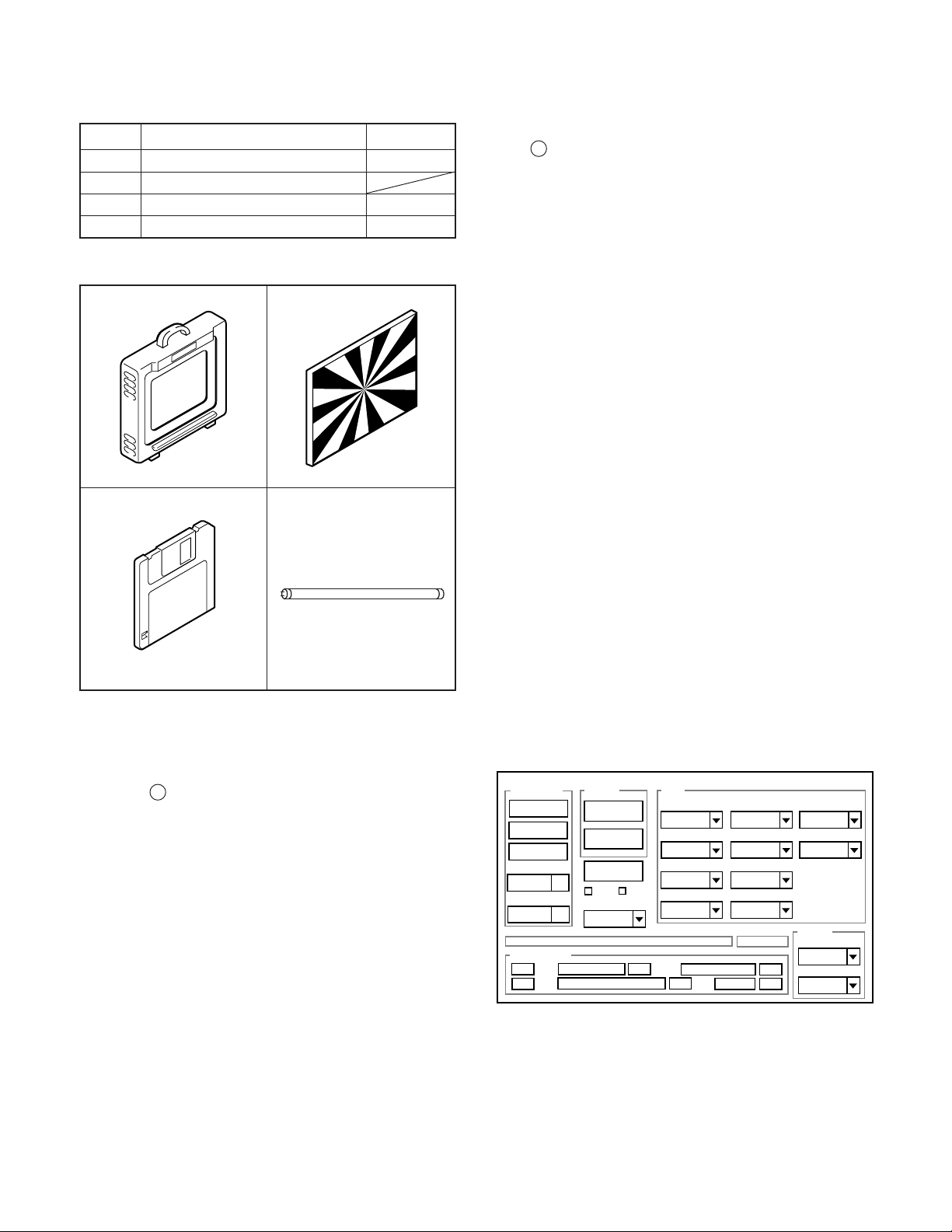
3-1. Table for Servicing Tools
Ref. No.
J-1
J-2
J-3
J-4
Note: J-1 color viewer is 100 - 110 VAC only.
Color viewer 5,100 K
Siemens star chart
Calibration software
Spare lamp
Name
Part code
VJ8-0007
VJ8-0184
VJ8-0028
3-4. Setup
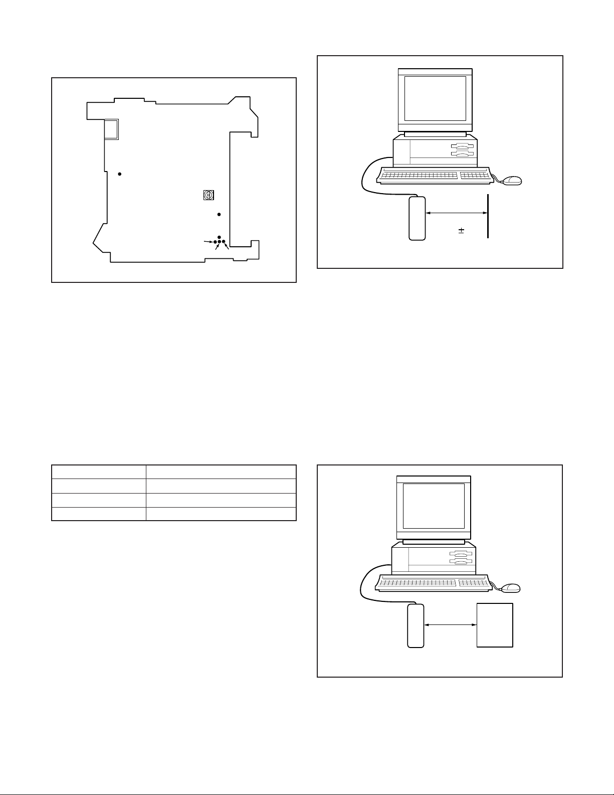
1. System requirements
Windows 98 or Me
IBM R -compatible PC with pentium processor
CD-ROM drive
3.5-inch high-density diskette drive
USB port
40 MB RAM
Hard disk drive with at least 15 MB available
VGA or SVGA monitor with at least 256-color display
J-1 J-2
J-3
J-4
3-2. Equipment
1. Oscilloscope
2. Digital voltmeter
3. AC adaptor
4. PC (IBM R -compatible PC, Pentium processor, Window
98 or Me)
3-3. Adjustment Items and Order
1. IC511 Oscillation Frequency Adjustment
2. Lens Adjustment
3. AWB Adjustment
4. Color Adjustment
5. CCD White Point Defect Detect Adjustment
6. CCD Black Point Defect Detect Adjustment
7. LCD Panel Adjustment
7-1. LCD H AFC Adjustment
7-2. LCD RGB Offset Adjustment
7-3. LCD Gain Adjustment
7-4. LCD Red Brightness Adjustment
7-5. LCD Blue Brightness Adjustment
Note: If the lens, CCD and board and changing the part in
item 2-6 replace, it is necessary to adjust again. Item 35 adjustments should be carried out in sequence. Item
6 adjustments should be carried out after item 3.
2. Installing calibration software
1. Insert the calibration software installation diskette into your
diskette drive.
2. Open the explorer.
3. Copy the DscCalDI_128 folder on the floppy disk in the FD
drive to a folder on the hard disk.
3. Installing USB drive
Install the USB drive with camera or connection kit for PC.
4. Color Viewer
1. Turn on the switch and wait for 30 minutes for aging to take
place before using Color Pure.
2. The luminance adjustment control on the color viewer
should be set to around the middle position (memory 5)
during use.
3. The fluorescent lamps which are used in the color viewer
are consumable parts. After the cumulative usage time
reaches 2000 hours, the color temperature will start to increase as the usage time increases, and correct adjustment will not be possible. When the cumulative usage time
reaches 2000 hours, all of the fluorescent lamps should be
simultaneously replaced with new lamps.
5. Computer screen during adjustment
Calibration
AWB
Focus
UV Matrix
Cal Mode
Cal Data
USB storage
VID
Get
PID
Set
OK
OK
Upload
Firmware
Image
Initialize
EVF
LCD Type
LCD
R Bright
RGB Offset
Tint
VCO
H AFC Test
Serial
Set
Set
Rev.
B Bright
Gain
Phase
Set
Set
VCOMDC
VCOMPP
Setting
Language
Video Mode
– 14 –
Page 15
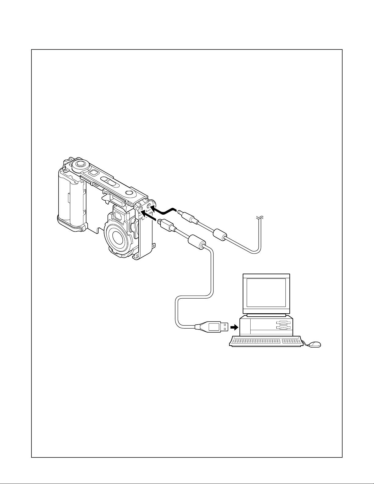
3-5. Connecting the camera to the computer
1. Line up the arrow on the cable connector with the notch on the camera's USB port. Insert the connector.
2. Locate a USB port on your computer.
USB cable
To USB port
AC adaptor
– 15 –
Page 16
3-6. Adjust Specifications
[CA3 board (Side A)]
CL578
VR513
CL407
(CSYNC)
CL402(G)
CL404
(XENB)
CL401(B)
Note:
1. Voltage adjustment is necessary to repair in the CA3 board
and replace the parts.
2. Power voltage set about +3.0 V.
Preparation:
1. Carry out the voltage adjustments disconnecting cabinet
back.
2. Insert the compact flash.
3. Set the main switch to the camera mode.
4. Set the selector dial to the still image shooting mode.
5. Push the power switch, and comfirm that the through screen
from the CCD can be seen on the LCD.
CL403(R)
2. Lens Adjustment
Camera
Preparation:
POWER switch: ON
Adjustment condition:
More than A3 size siemens star chart
Fluorescent light illumination with no flicker
Illumination above the subject should be 400 lux ± 10 %.
Adjustment method:
1. Set the siemens star chart 150 cm ± 3 cm so that it becomes center of the screen.
2. Double-click on the DscCalDi128.
3. Click the Focus, and click the Yes.
4. Lens adjustment value will appear on the screen.
5. Click the OK.
Approx.
150 cm 3 cm
Siemens
star chart
1. IC511 Oscillation Frequency Adjustment
Measuring Point
Measuring Equipment
ADJ. Location
ADJ. Value
Adjustment method:
1. Adjust with VR513 to 495 ± 2 kHz.
CL578
Frequency counter
VR513
495 ± 2 kHz
3. AWB Adjustment
Camera
All white pattern
Color viewer
Preparation:
POWER switch: ON
Adjusting method:
1. When setting the camera in place, set it to an angle so that
nothing appears in any part of the color viewer except the
white section. (Do not enter any light.)
– 16 –
Page 17

2. Double-click on the DscCalDi128.
3. Click the AWB, and click the Yes.
4. AWB adjustment value will appear on the screen.
5. Click the OK.
4. Color Adjustment
6. CCD Black Point Defect Detect Adjustment
Camera
All white pattern
Color viewer
Camera
All white pattern color
viewer and color matrix
adjustment chart
Preparation:
POWER switch: ON
Adjustment method:
1. Set the color adjustment chart to the color viewer.
(Do not enter any light.)
2. Set the color adjustment chart so that it becomes center
of the screen.
3. Double-click on the DscCalDi128.
4. Click the “UV Matrix”, and Click the “Ye s ”.
5. Adjustment values will appear on the screen.
6. Click the OK.
5. CCD White Point Defect Detect Adjustment
Preparation:
POWER switch: ON
Adjustment method:
1. Double-click on the DscCalDi128.
2. Select “CCD Defect” on the LCD “Test”, and click the “Ye s ”.
3. After the adjustment is completed, the number of defect
will appear.
Preparation:
POWER switch: ON
Adjusting method:
1. When setting the camera in place, set it to an angle so
that nothing appears in any part of the color viewer except the white section. (Do not enter any light.)
2. Double-click on the DscCalDi128.
3. Select “CCD Black” on the LCD “Test”, and click the “Ye s ”.
4. After the adjustment is completed, the number of defect
will appear.
7. LCD Panel Adjustment
[CA3 board (Side A)]
CL578
VR513
CL407
(CSYNC)
CL402(G)
CL404
(XENB)
CL401(B)
CL403(R)
7-1. LCD H AFC Adjustment
Preparation:
POWER switch: ON
Adjusting method:
1. Double-click on the DscCalDi128.
2. Select 0 on the LCD “H AFC”.
3. Apply a trigger using CL407, and adjust LCD “H AFC” so
that the time A from the rising signal at CL407 to the falling signal at CL404 is 5.26 ± 0.2 µsec.
– 17 –
Page 18

○○○○○○○○
○○
A
CL404
CL407
Enlargement
○○○○○○○○
○○
A
CL404
CL407
7-2. LCD RGB Offset Adjustment
Adjusting method:
1. Adjust LCD “RGB Offset” so that the amplitude of the CL402
waveform is 4.0 V ± 0.1 Vp-p.
Note:
7-2. LCD RGB Offset adjustment and 7-3. LCD Gain adjustment should always be carried out first.
VG
CL402 waveform
(VG–0.1) ±
0.05 Vp-p
4.0 V ±
0.1 Vp-p
CL402 waveform
7-3. LCD Gain Adjustment
Adjusting method:
1. Adjust LCD “Gain” so that the amplitude of the CL402 wave-
form is 7.3 V ± 0.3 Vp-p.
Note:
7-2. LCD RGB Offset adjustment should always be carried
out first.
7.3 V ±
0.3 Vp-p
CL403 waveform
7-5. LCD Blue Brightness Adjustment
Adjusting method:
1. Adjust LCD “B Bright” so that the amplitude of the CL401
waveform is (VG+0.2) ± 0.05 Vp-p with respect to the CL402
(VG) waveform.
Note:
7-2. LCD RGB Offset adjustment and 7-3. LCD Gain adjustment have done.
VG
CL402 waveform
CL402 waveform
7-4. LCD Red Brightness Adjustment
Adjusting method:
1. Adjust LCD “R Bright” so that the amplitude of the CL403
waveform is (VG–0.1) ± 0.05 Vp-p with respect to the CL402
(VG) waveform.
(VG+0.2) ±
0.05Vp-p
CL401 waveform
– 18 –
Page 19

4. USB STORAGE INFORMATION
REGISTRATION
USB storage data is important for when the camera is connected to a computer via a USB connection.
If there are any errors in the USB storage data, or if it has not
been saved, the USB specification conditions will not be satisfied, so always check and save the USB storage data.
Preparation:
POWER switch: ON
Adjustment method:
1. Connect the camera to a computer. (Refer to 3-5. Connecting the camera to the computer on the page 15.)
2. Double-click on the DscCalDi128.
3. Click on the Get button in the USB storage window and
check the USB storage data.
VID: SANYO
PID: VPC-AZ1EX or VPC-AZ1E or VPC-AZ1
Serial:
Rev. : 1.00
4. Check the “Serial” in the above USB storage data. If the
displayed value is different from the serial number printed
on the base of the camera, enter the number on the base
of the camera. Then click the Set button.
5. Next, check VID, PID and Rev. entries in the USB storage
data. If any of them are different from the values in 3. above,
make the changes and then click the corresponding Set
button.
Calibration
AWB
Focus
UV Matrix
Cal Mode
Cal Data
USB storage
VID
Get
PID
Set
OK
OK
Upload
Firmware
Image
Initialize
EVF
LCD Type
LCD
R Bright
RGB Offset
Tint
VCO
H AFC Test
Serial
Set
Set
Rev.
B Bright
Gain
Phase
Set
Set
VCOMDC
VCOMPP
Setting
Language
Video Mode
– 19 –
Page 20

5. TROUBLESHOOTING GUIDE
POWER LOSS INOPERTIVE
PUSH MAIN SW
IC301-46 (SCAN IN 5)
PULSE INPUT
YES
IC302-7 (UNREG)
HIGH
IC301-10
(VDD)
HIGH
IC301-36
(RESET)
HIGH
IC301-43
(BAT OFF)
HIGH
IC301-40
OSCILLATION
YES
IC301-37
OSCILLATION
YES
NO
LOW
CHECK PW1, IC303
LOW
LOW
CHECK IC302, R3006
LOW
NO
NO
CHECK
S3002, R3055
CHECK IC302
CHECK R3007
CHECK X3001
CHECK X3002
TAKING INOPERATIVE
PUSH SHUTTER
BUTTON
IC301-53, 46
(SCAN IN 4, 5)
PULSE INPUT
YES
CN301-5, 6
(P ON, P(A) ON)
HIGH
SERIAL
COMMUNICATION
OK
CHECK CA2
NO
LOW
R3023, R3024, PW1
NG
CHECK R3054,
R3055, D3012
CHECK IC301,
CHECK
IC301, CA2
CHECK IC301
NO PICTURE
CLK (96 MHz)
INPUT TO
IC102-283 (CLK IN 1)
NO
CLK (36 MHz)
INPUT TO
IC101-132 (CLK IN 1)
OK
IC101-61 (ZAS)
OK
IC101-118, 119
(IRL1, 2)
OK
CHECK SOLDERING OF
EACH CPU AND
MEMORY PIN
MAIN CLOCK FOR SYSTEM OPERATION
YES
NO OPERATION IF ABSENT
CHECK X1101 OSCILLATOR AND IC111
NG
BASIC CPU BLOCK
CHECK IC102-272
ALWAYS APPEARS WHEN CPU, ETC. IS ACCESSED
NG
CHECK IF CPU IS READKING PROGRAM, AND
CHECK ADDRESS AND DATA BUS OF IC121
INCORRECT HANDSHAKING BETWEEN 8-BIT
NG
CPU AND RS-232C
CHECK EACH INTERFACE
– 20 –
Page 21

6. PARTS LIST
LOCATION PARTS NO. DESCRIPTION LOCATION PARTS NO. DESCRIPTION
CABINET AND CHASSIS PARTS 1
1 636 063 7641 CABINET FRONT-SX511/EX
2 636 063 8105 DEC GRIP-SX511/J
3 636 062 8540 SPACER FRONT-SX212
4 636 061 4208 DEC FLASH-SX212/J
5 636 063 0222 SHILED TAPE-SX212/J
6 636 063 6378 ASSY,COVER LENS-SX511/J
7 636 065 6253 SPACER COVER LENS B-212/J
8 636 065 6246 SPACER COVER LENS A-212/J
9 636 061 4130 CABINET FRONT INNER-212/J
10 645 045 9214 MICROPHONE
11 636 064 8753 HOLDER MIC-SX212/J
12 636 062 8502 ADHESIVE TAPE FRONT A-212
13 636 062 8519 ADHESIVE TAPE FRONT B-212
14 636 062 9974 SPACER A-SX212/J
15 636 063 3223 LEVER COVER LENS-SX212/J
16 636 062 8564 SPRING COVER LENS B-SX212
17 645 046 9121 ASSY,MOTOR
18 636 063 3919 COMPL PWB,SY-2
19 636 063 6538 COVER JACK-SX511/J
20 636 063 6484 CABINET LEFT-SX511/J
21 645 037 0274 PAD(L=15)
22 636 063 2745 SPACER UNIT-SX212/J
23 645 050 3641 UNIT,CONTROL PANEL SX511
24 636 063 7603 ASSY,CABINET TOP-SX511/EX
25 636 063 6613 KNOB FUNCTION-SX511/J
26 636 061 4307 SLIDE FUNCTION-SX212/J
27 636 061 3447 HOLDER MONITOR-SX212/J
28 636 064 7640 SPACER HL MONITOR-SX511/J
29 645 045 8590 LCD(ALP228CGXC0)
30 636 061 4291 SPACER MONTOR-SX212/J
31 636 063 7634 CABINET BACK-SX511/EX
32 636 061 9210 DEC MONITOR-SX511/J
33 636 061 5175 ASSY,COVER EYE-SX212/J
34 636 063 1298 SPACER MIC-SX212
35 636 063 4954 SPACER B-SX212
36 636 064 7831 SPACER CABI BACK-SX511/J
101 411 177 6502 SCR S-TPG PAN PCS 1.7X4
102 411 176 7005 SCR S-TPG PAN PCS 1.7X5.0
103 412 064 1808 SPECIAL SCREW-1.7X4
104 412 060 9501 SPECIAL SCREW-1.7X2.5
105 411 175 8904 SCR PAN PCS 1.7X3.5
106 411 177 8407 SCR S-TPG PAN PCS 1.7X3
107 411 177 8100 SCR S-TPG PAN PCS 1.7X2.5
104
107
23
22
14
25
26
106
105
24
101
101
27
36
30
101
19
31
35
29
28
103
5
32
18
33
103
102
103
2
21
15
17
20
103
14
3
4
13
16
101
8
12
9
6
7
10
11
SX511/J Parts List-1
N.S.P.: Not available as service parts.
1
103
5
103
34
21
Page 22

LOCATION PARTS NO. DESCRIPTION LOCATION PARTS NO. DESCRIPTION
CABINET AND CHASSIS PARTS 2
1 645 050 7885 LENS(ASSY),R127E
2 636 062 9813 SPACER LENS-SX212/J
3 645 051 4913 OPTICAL FILTER
4 636 057 0696 SPACER
5 409 505 6003 IC ICX411AK-C
6 636 061 5298 MOUNTING,LENS
7 636 061 5304 SPACER INSULATOR
8 636 060 9785 SHILED TAPE SX212
9 636 063 2981 COMPL PWB,CA-1
10 636 063 3971 COMPL PWB,PW-1
11 645 046 9343 ASSY,LAMP,SX212
12 636 061 3768 HOLDER FLASH-SX212/J, HOLDER_FLASH
13 636 063 6514 COVER BATTETY-SX511/J
14 636 061 4161 CAP BATT TERMINAL-SX212/J
15 636 062 9738 ASSY,HOLDER CV BATT-SX212
16 636 063 6606 HOLDER COVER BATT-SX511/J
17 636 065 8172 ASSY,HLD BATT B-SX511J SV
18 636 063 2974 COMPL PWB,CA-2,VPC-AZ1 ONLY
18 636 063 3001 COMPL PWB,CA-2,EXCEPT VPC-AZ1
19 645 045 9290 FLEXIBLE FLAT CABLE
38
17
(Included in the COMPL PWB PW-1)
(Included in the COMPL PWB PW-1)
30
32
29
28
27
101
31
26
20 636 063 6620 STAND-SX511/J, STAND
21 636 061 5335 SPACER SPEAKER A-SX212/J
22 645 045 9207 SPEAKER,8
23 636 061 3775 HOLDER SPEAKER-SX212/J
24 636 061 3744 HOLDER LENS-SX212/J
25 645 041 3148 PAD(L=12)
26 636 061 3454 HOLDER CHASSIS-SX212/J
27 636 061 8893 SPACER CHASSIS M-SX212/J
28 636 063 7511 SHAFT CARD-SX212/J
29 636 063 6507 COVER CARD-SX511/J
30 636 063 6576 HOLDER CARD-SX511/J
31 636 061 3836 SHAFT STRAP-SX212/J
32 636 063 3902 COMPL PWB,SY-1
33 636 063 3896 COMPL PWB,CA-3
34 636 061 5342 SPACER SPEAKER B-SX212/J
35 636 064 8234 SHILED TAPE CA1-LENSSX511
36 636 064 8241 SHILED TAPE CA1-LENSSX511
37 636 064 9743 SPACER FLASH-SX511/J
38 636 062 9974 SPACER A-SX212/J
39 645 052 2130 PAD(L=10)
101 411 177 6502 SCR S-TPG PAN PCS 1.7X4
105 411 175 8904 SCR PAN PCS 1.7X3.5
107 411 177 8100 SCR S-TPG PAN PCS 1.7X2.5
108 411 182 3701 SCRS-TPG PAN PCS 1.7X5
101
101
105
105
107
16
15
14
13
101
SX511/J Parts List-2
107
107
101
101
18
101
12
11
37
25
39
101
33
24
23
34
19
107
22
20
10
2
6
5
4
3
101
1
N.S.P.: Not available as service parts.
21
35
108
36
8
9
7
22
Page 23

ELECTRICAL PARTS
Note:
1. Materials of Capacitors and Resistors are abbreviated as follows ;
Resistors Capacitors
MT-FILM Metallized Film Resistor MT-POLYEST Metallized Polyester Capacitor
MT-GLAZE Metallized Glaze Resistor MT-COMPO Metallized Composite Capacitor
OXIDE-MT Oxide Metallized Film Resistor TA-SOLD Tantalum Solid Capacitor
AL-SOLID Aluminum Solid Capacitor
NP-ELECT Non-Polarized Electrolytic Capacitor
OS-SOLID Aluminum Solid Capacitors with Organic
2. Tolerance of Capacitor (10pF over) and Resistor are noted with follow symboles.
DL-ELECT Double Layered Electrolytic Capacitor
F ............1% G ............2% J ............5% K ............10%
M ..........20% N ..........30% Z ..........+80% ~ -20%
3. Capacitors
µ
F P : pF
U :
4. Inductors
µ
H MH : mH
UH :
5. N.S.P. : Not available as service parts.
LOCATION PARTS NO. DESCRIPTION LOCATION PARTS NO. DESCRIPTION
COMPL PWB,CA-1
636 063 2981
(SEMICONDUCTORS)
Q9001 405 102 5609 TR 2SD1819A-R
OR 405 092 4101 TR 2SC4081-R
Q9002 405 102 5609 TR 2SD1819A-R
OR 405 092 4101 TR 2SC4081-R
Q9003 405 153 6709 TR 2SC3931-D
(INTEGRATED CIRCUIT)
IC901 409 446 8708 IC CXD3400N
(DIODES)
D9001 407 205 2707 LED SML-310LT,
D9002 407 113 5609 DIODE DSH015
OR 407 134 7200 DIODE MA141K
D9003 407 198 9905 DIODE MA727
D9004 407 198 9905 DIODE MA727
D9005 407 222 4807 LED SML-521MUW,
(CAPACITORS)
C9001 403 320 5500 CERAMIC 1U Z 25V
C9002 403 312 6805 CERAMIC 0.1U Z 16V
C9003 403 283 6309 CERAMIC 1U Z 10V
C9005 403 283 6309 CERAMIC 1U Z 10V
C9006 403 283 6309 CERAMIC 1U Z 10V
C9007 403 311 3409 CERAMIC 0.01U K 16V
C9008 403 311 3409 CERAMIC 0.01U K 16V
C9009 403 312 6805 CERAMIC 0.1U Z 16V
C9010 403 320 5500 CERAMIC 1U Z 25V
C9011 403 312 6805 CERAMIC 0.1U Z 16V
C9012 403 312 6805 CERAMIC 0.1U Z 16V
C9013 403 312 6805 CERAMIC 0.1U Z 16V
C9014 403 312 6805 CERAMIC 0.1U Z 16V
C9015 403 283 6309 CERAMIC 1U Z 10V
C9016 403 283 6309 CERAMIC 1U Z 10V
C9017 403 332 8209 CERAMIC 10U M 16V
C9018 403 312 6805 CERAMIC 0.1U Z 16V
C9019 403 312 6805 CERAMIC 0.1U Z 16V
C9020 403 155 1807 CERAMIC 0.01U K 25V
C9021 403 320 5500 CERAMIC 1U Z 25V
C9023 403 164 0204 CERAMIC 0.1U Z 25V
(RESISTORS)
R9001 401 225 1306 MT-GLAZE 470 JA 1/16W
R9002 401 224 8900 MT-GLAZE 100K JA 1/16W
R9003 401 261 5900 MT-FILM 330 DU 1/16W
R9004 401 261 3906 MT-FILM 2.2K DU 1/16W
R9014 401 224 9402 MT-GLAZE 1.0M JA 1/16W
R9015 401 224 9006 MT-GLAZE 10K JA 1/16W
R9016 401 240 9004 MT-GLAZE 3.9 JA 1/16W
R9017 401 225 0903 MT-GLAZE 82K JA 1/16W
R9018 401 224 9006 MT-GLAZE 10K JA 1/16W
R9019 401 261 1001 MT-GLAZE 2.4K JA 1/16W
R9021 401 224 8801 MT-GLAZE 100 JA 1/16W
R9022 401 225 0200 MT-GLAZE 3.3K JA 1/16W
CN901 645 045 4424 SOCKET,26P (N.S.P)
CN902 645 027 5340 PLUG,3P (N.S.P)
COMPL PWB,CA-2
Q1001 405 115 5702 TR DTA144EE
Q1301 405 129 2001 TR UMH2N
Q1302 405 129 3107 TR UMD3N
Q1303 405 115 7201 TR DTC144EE
Q1304 405 115 7201 TR DTC144EE
Q1401 405 115 5702 TR DTA144EE
Q1402 405 115 7201 TR DTC144EE
Q1501 405 129 2100 TR UMT1N
Q1502 405 129 2308 TR UMZ1N
OR 405 106 4806 TR XP4601
Q1503 405 102 6705 TR 2SA1745-7
OR 405 102 8303 TR 2SA1745-6
Q1504 405 115 7201 TR DTC144EE
Q1505 405 129 2308 TR UMZ1N
OR 405 106 4806 TR XP4601
Q1601 405 115 7201 TR DTC144EE
Q1602 405 102 6705 TR 2SA1745-7
OR 405 102 8303 TR 2SA1745-6
Q1801 405 129 2209 TR UMX1N
Q1802 405 102 5609 TR 2SD1819A-R
OR 405 092 4101 TR 2SC4081-R
Q1803 405 115 5702 TR DTA144EE
Q9101 405 115 7201 TR DTC144EE
IC101 409 509 5507 IC MB86838PBT2-G (N.S.P.)
IC102 410 412 9100 IC KS6M0U1453CBP (N.S.P.)
IC103 409 497 3202 IC TC59SM716AFT-80
IC104 409 497 3202 IC TC59SM716AFT-80
IC105 409 471 4003 IC SN74LV273ADB
IC106 409 471 4003 IC SN74LV273ADB
IC107 409 471 4003 IC SN74LV273ADB
IC108 409 305 3103 IC TC7W74FU
IC109 409 305 3103 IC TC7W74FU
IC111 409 486 8300 IC BU2381FV
IC121 409 515 6307 IC 29900511G
IC141 409 327 6502 IC TC7W32FU
IC152 409 427 4101 IC TK15405M
IC161 645 048 6074 UNIT,SENSOR-SX511
IC181 409 432 2505 IC LMV321M7X
IC182 409 432 2505 IC LMV321M7X
IC183 409 407 0505 IC TK11331BM
IC184 409 432 2505 IC LMV321M7X
IC185 409 395 5902 IC TC7SH00FU
(CONNECTORS)
(MISCELLANEOUS)
636 064 8180 SPACER,CA1-SX511
6360632974 (VPC-AZ1 ONLY)
6360633001 (EXCEPT VPC-AZ1)
(SEMICONDUCTORS)
(INTEGRATED CIRCUITS)
Semiconductive Electrolytic Capacitor
23
Page 24

LOCATION PARTS NO. DESCRIPTION LOCATION PARTS NO. DESCRIPTION
IC186 409 301 5507 IC TC7S08FU
IC911 409 506 3100 IC AD9849KST
IC912 409 407 0505 IC TK11331BM
(DIODES)
D1001 407 134 7408 DIODE MA141WK
OR 407 130 4401 DIODE DAN202U
D1501 407 109 4609 DIODE MA728
D1801 407 188 9809 DIODE MA742
D1802 407 149 0807 DIODE 1SS355
(OSCILLATORS)
X1101 645 023 3951 OSC,CRYSTAL 14.31818MHZ
OR 645 040 0049 OSC,CRYSTAL 14.31818MHZ
(INDUCTORS)
L1001 645 020 1912 INDUCTOR,240 OHM
L1002 645 020 1912 INDUCTOR,240 OHM
L1003 645 021 1737 INDUCTOR,47U J
OR 645 043 5898 INDUCTOR,47U J
L1101 645 020 1899 INDUCTOR,68 OHM
L1102 645 020 1899 INDUCTOR,68 OHM
L1103 645 020 1912 INDUCTOR,240 OHM
L1301 645 020 1851 INDUCTOR,1000 OHM
L1302 645 020 1851 INDUCTOR,1000 OHM
L1303 645 020 1851 INDUCTOR,1000 OHM
L1501 645 035 7190 INDUCTOR,33U J
L1601 645 016 0349 INDUCTOR,600 OHM
L1602 645 016 0349 INDUCTOR,600 OHM
L1603 645 016 0349 INDUCTOR,600 OHM
L1604 645 016 0349 INDUCTOR,600 OHM
(FILTER)
L9101 645 045 3236 FILTER,EMI 1000PF
(CAPACITORS)
C1001 403 345 4304 TA-SOLID 22U M 10V
C1002 403 345 4205 TA-SOLID 47U M 6.3V
C1003 403 312 6805 CERAMIC 0.1U Z 16V
C1004 403 312 6805 CERAMIC 0.1U Z 16V
C1005 403 312 6805 CERAMIC 0.1U Z 16V
C1007 403 312 6805 CERAMIC 0.1U Z 16V
C1010 403 312 6805 CERAMIC 0.1U Z 16V
C1012 403 312 6805 CERAMIC 0.1U Z 16V
C1014 403 312 6805 CERAMIC 0.1U Z 16V
C1016 403 312 6805 CERAMIC 0.1U Z 16V
C1033 403 283 6309 CERAMIC 1U Z 10V
C1034 403 312 6805 CERAMIC 0.1U Z 16V
C1035 403 283 6309 CERAMIC 1U Z 10V
C1036 403 312 6805 CERAMIC 0.1U Z 16V
C1037 403 283 6309 CERAMIC 1U Z 10V
C1038 403 312 6805 CERAMIC 0.1U Z 16V
C1039 403 283 6309 CERAMIC 1U Z 10V
C1040 403 312 6805 CERAMIC 0.1U Z 16V
C1045 403 283 6309 CERAMIC 1U Z 10V
C1046 403 312 6805 CERAMIC 0.1U Z 16V
C1048 403 283 6309 CERAMIC 1U Z 10V
C1050 403 346 2309 CERAMIC 0.1U K 10V
C1051 403 346 2309 CERAMIC 0.1U K 10V
C1052 403 346 2309 CERAMIC 0.1U K 10V
C1053 403 283 6309 CERAMIC 1U Z 10V
C1055 403 346 2309 CERAMIC 0.1U K 10V
C1056 403 346 2309 CERAMIC 0.1U K 10V
C1057 403 346 2309 CERAMIC 0.1U K 10V
C1058 403 338 4403 CERAMIC 0.1U K 16V
C1059 403 338 4403 CERAMIC 0.1U K 16V
C1060 403 338 4403 CERAMIC 0.1U K 16V
C1062 403 283 6309 CERAMIC 1U Z 10V
C1063 403 312 6805 CERAMIC 0.1U Z 16V
C1064 403 283 6309 CERAMIC 1U Z 10V
C1065 403 283 6309 CERAMIC 1U Z 10V
C1066 403 283 6309 CERAMIC 1U Z 10V
C1067 403 311 4505 CERAMIC 1000P K 50V
C1068 403 311 4505 CERAMIC 1000P K 50V
C1069 403 311 4505 CERAMIC 1000P K 50V
C1101 403 309 8409 CERAMIC 10P D 50V
C1104 403 343 3101 CERAMIC 1U K 6.3V
C1105 403 311 3409 CERAMIC 0.01U K 16V
C1106 403 311 3409 CERAMIC 0.01U K 16V
C1107 403 311 3409 CERAMIC 0.01U K 16V
C1201 403 283 6309 CERAMIC 1U Z 10V
C1306 403 323 6207 CERAMIC 1U K 10V
C1401 403 312 6805 CERAMIC 0.1U Z 16V
C1402 403 312 6805 CERAMIC 0.1U Z 16V
C1403 403 329 6508 TA-SOLID 10U M 6.3V
C1404 403 312 6805 CERAMIC 0.1U Z 16V
C1501 403 311 5007 CERAMIC 33P J 50V
C1502 403 311 7506 CERAMIC 22P J 50V
C1504 403 343 3101 CERAMIC 1U K 6.3V
C1505 403 343 3101 CERAMIC 1U K 6.3V
C1506 403 345 4205 TA-SOLID 47U M 6.3V
C1507 403 345 3802 TA-SOLID 22U M 4V
C1508 403 283 6309 CERAMIC 1U Z 10V
C1801 403 346 2309 CERAMIC 0.1U K 10V
C1802 403 311 3409 CERAMIC 0.01U K 16V
C1803 403 344 0505 CERAMIC 0.033U K 10V
C1804 403 155 1807 CERAMIC 0.01U K 25V
C1805 403 283 6309 CERAMIC 1U Z 10V
C1806 403 283 6309 CERAMIC 1U Z 10V
C1807 403 346 2309 CERAMIC 0.1U K 10V
C1808 403 283 6309 CERAMIC 1U Z 10V
C1809 403 319 3609 CERAMIC 330P K 50V
C1810 403 283 6309 CERAMIC 1U Z 10V
C1811 403 343 3101 CERAMIC 1U K 6.3V
C1812 403 343 3101 CERAMIC 1U K 6.3V
C1813 403 329 6508 TA-SOLID 10U M 6.3V
C1814 403 311 3409 CERAMIC 0.01U K 16V
C1815 403 283 6309 CERAMIC 1U Z 10V
C1816 403 319 3609 CERAMIC 330P K 50V
C1817 403 283 6309 CERAMIC 1U Z 10V
C1818 403 283 6309 CERAMIC 1U Z 10V
C1819 403 283 6309 CERAMIC 1U Z 10V
C1820 403 343 3101 CERAMIC 1U K 6.3V
C9101 403 311 3409 CERAMIC 0.01U K 16V
C9102 403 283 6309 CERAMIC 1U Z 10V
C9103 403 283 6309 CERAMIC 1U Z 10V
C9105 403 346 2309 CERAMIC 0.1U K 10V
C9106 403 269 2806 CERAMIC 0.15U K 25V
C9107 403 346 2309 CERAMIC 0.1U K 10V
C9108 403 343 3101 CERAMIC 1U K 6.3V
C9109 403 311 3409 CERAMIC 0.01U K 16V
C9110 403 343 3101 CERAMIC 1U K 6.3V
C9111 403 311 3409 CERAMIC 0.01U K 16V
C9112 403 346 2309 CERAMIC 0.1U K 10V
C9113 403 346 2309 CERAMIC 0.1U K 10V
C9114 403 346 2309 CERAMIC 0.1U K 10V
C9115 403 346 2309 CERAMIC 0.1U K 10V
C9116 403 345 4304 TA-SOLID 22U M 10V
C9117 403 311 3409 CERAMIC 0.01U K 16V
C9118 403 346 2309 CERAMIC 0.1U K 10V
C9119 403 346 2309 CERAMIC 0.1U K 10V
C9120 403 346 2309 CERAMIC 0.1U K 10V
C9121 403 345 4304 TA-SOLID 22U M 10V
C9122 403 311 3409 CERAMIC 0.01U K 16V
C9123 403 207 0307 CERAMIC 1U Z 16V
(RESISTORS)
R1001 401 224 9006 MT-GLAZE 10K JA 1/16W
R1002 401 224 9006 MT-GLAZE 10K JA 1/16W
R1004 401 224 9006 MT-GLAZE 10K JA 1/16W
R1007 401 105 5103 MT-GLAZE 47 JA 1/16W
R1008 401 225 7902 MT-GLAZE 220 JA 1/16W
R1009 401 225 7902 MT-GLAZE 220 JA 1/16W
R1010 401 225 7902 MT-GLAZE 220 JA 1/16W
R1011 401 224 9006 MT-GLAZE 10K JA 1/16W
R1012 401 224 9006 MT-GLAZE 10K JA 1/16W
R1015 401 224 9006 MT-GLAZE 10K JA 1/16W
R1016 401 226 1503 MT-GLAZE 0.000 ZA 1/16W
R1017 401 224 8801 MT-GLAZE 100 JA 1/16W
R1018 401 225 7902 MT-GLAZE 220 JA 1/16W
R1022 401 225 7902 MT-GLAZE 220 JA 1/16W
R1023 401 225 7902 MT-GLAZE 220 JA 1/16W
R1024 401 225 7902 MT-GLAZE 220 JA 1/16W
R1025 401 225 7902 MT-GLAZE 220 JA 1/16W
R1026 401 225 7902 MT-GLAZE 220 JA 1/16W
R1027 401 225 7902 MT-GLAZE 220 JA 1/16W
R1028 401 225 7902 MT-GLAZE 220 JA 1/16W
R1029 401 225 7902 MT-GLAZE 220 JA 1/16W
R1030 401 225 7902 MT-GLAZE 220 JA 1/16W
R1031 401 225 7902 MT-GLAZE 220 JA 1/16W
R1032 401 225 7902 MT-GLAZE 220 JA 1/16W
R1037 401 237 2308 MT-GLAZE 910 JA 1/16W
24
Page 25

LOCATION PARTS NO. DESCRIPTION LOCATION PARTS NO. DESCRIPTION
R1038 401 261 5108 MT-FILM 1.0K DU 1/16W
R1039 401 261 3401 MT-FILM 3.6K DU 1/16W
R1040 401 261 5108 MT-FILM 1.0K DU 1/16W
R1042 401 224 9006 MT-GLAZE 10K JA 1/16W
R1046 401 224 9303 MT-GLAZE 1K JA 1/16W
R1047 401 224 9006 MT-GLAZE 10K JA 1/16W
R1048 401 224 9006 MT-GLAZE 10K JA 1/16W
R1049 401 224 9006 MT-GLAZE 10K JA 1/16W
R1101 401 225 0309 MT-GLAZE 33 JA 1/16W
R1102 401 225 0309 MT-GLAZE 33 JA 1/16W
R1103 401 224 8801 MT-GLAZE 100 JA 1/16W
R1201 401 225 8107 MT-GLAZE 10 JA 1/16W
R1302 401 226 1503 MT-GLAZE 0.000 ZA 1/16W
R1303 401 224 9006 MT-GLAZE 10K JA 1/16W
R1304 401 224 9006 MT-GLAZE 10K JA 1/16W
R1305 401 224 8900 MT-GLAZE 100K JA 1/16W
R1306 401 224 9006 MT-GLAZE 10K JA 1/16W
R1307 401 225 3805 MT-GLAZE 1.5K JA 1/16W
R1308 401 225 1108 MT-GLAZE 27 JA 1/16W
R1309 401 225 1108 MT-GLAZE 27 JA 1/16W
R1310 401 226 1503 MT-GLAZE 0.000 ZA 1/16W
R1311 401 226 1503 MT-GLAZE 0.000 ZA 1/16W
R1401 401 224 9006 MT-GLAZE 10K JA 1/16W
R1402 401 224 9006 MT-GLAZE 10K JA 1/16W
R1403 401 224 9006 MT-GLAZE 10K JA 1/16W
R1404 401 224 9006 MT-GLAZE 10K JA 1/16W
R1405 401 224 9006 MT-GLAZE 10K JA 1/16W
R1406 401 224 9006 MT-GLAZE 10K JA 1/16W
R1407 401 224 9006 MT-GLAZE 10K JA 1/16W
R1408 401 226 1503 MT-GLAZE 0.000 ZA 1/16W
R1409 401 225 1405 MT-GLAZE 47K JA 1/16W
R1410 401 224 8900 MT-GLAZE 100K JA 1/16W
R1501 401 261 9908 MT-FILM 91 DD 1/16W
R1502 401 261 7102 MT-FILM 150 DU 1/16W
R1503 401 225 3805 MT-GLAZE 1.5K JA 1/16W
R1504 401 262 0409 MT-FILM 56 DD 1/16W
R1505 401 261 6105 MT-FILM 390 DU 1/16W
R1506 401 261 5504 MT-FILM 560 DU 1/16W
R1507 401 226 2401 MT-GLAZE 560 JA 1/16W
R1509 401 224 9006 MT-GLAZE 10K JA 1/16W
R1510 401 225 3805 MT-GLAZE 1.5K JA 1/16W
R1511 401 261 6105 MT-FILM 390 DU 1/16W
R1512 401 261 3807 MT-FILM 2.0K DU 1/16W
R1513 401 261 5108 MT-FILM 1.0K DU 1/16W
R1514 401 261 5108 MT-FILM 1.0K DU 1/16W
R1515 401 226 5402 MT-GLAZE 56 JA 1/16W
R1516 401 225 2006 MT-GLAZE 680 JA 1/16W
R1517 401 226 1503 MT-GLAZE 0.000 ZA 1/16W
R1518 401 224 8900 MT-GLAZE 100K JA 1/16W
R1519 401 261 9601 MT-FILM 68 DD 1/16W
R1602 401 225 1207 MT-GLAZE 4.7K JA 1/16W
R1603 401 225 1207 MT-GLAZE 4.7K JA 1/16W
R1801 401 261 6303 MT-FILM 180 DU 1/16W
R1802 401 225 1207 MT-GLAZE 4.7K JA 1/16W
R1803 401 225 0408 MT-GLAZE 330K JA 1/16W
R1804 401 225 0408 MT-GLAZE 330K JA 1/16W
R1805 401 225 0200 MT-GLAZE 3.3K JA 1/16W
R1806 401 225 0200 MT-GLAZE 3.3K JA 1/16W
R1807 401 224 9303 MT-GLAZE 1K JA 1/16W
R1809 401 224 9006 MT-GLAZE 10K JA 1/16W
R1810 401 224 9006 MT-GLAZE 10K JA 1/16W
R1811 401 224 9006 MT-GLAZE 10K JA 1/16W
R1812 401 229 7205 MT-GLAZE 18K JA 1/16W
R1813 401 224 9501 MT-GLAZE 2.2K JA 1/16W
R1814 401 225 0408 MT-GLAZE 330K JA 1/16W
R1816 401 224 9501 MT-GLAZE 2.2K JA 1/16W
R1817 401 224 9006 MT-GLAZE 10K JA 1/16W
R1818 401 225 0408 MT-GLAZE 330K JA 1/16W
R1819 401 225 0606 MT-GLAZE 5.6K JA 1/16W
R1820 401 229 7205 MT-GLAZE 18K JA 1/16W
R1821 401 225 2105 MT-GLAZE 12K JA 1/16W
R1822 401 224 9303 MT-GLAZE 1K JA 1/16W
R1823 401 224 9808 MT-GLAZE 220K JA 1/16W
R1824 401 224 9006 MT-GLAZE 10K JA 1/16W
R1826 401 226 1503 MT-GLAZE 0.000 ZA 1/16W
R9101 401 224 8900 MT-GLAZE 100K JA 1/16W
R9102 401 226 1503 MT-GLAZE 0.000 ZA 1/16W
R9106 401 224 8801 MT-GLAZE 100 JA 1/16W
R9107 401 224 8801 MT-GLAZE 100 JA 1/16W
R9108 401 224 8801 MT-GLAZE 100 JA 1/16W
R9109 401 224 8801 MT-GLAZE 100 JA 1/16W
R9110 401 224 8801 MT-GLAZE 100 JA 1/16W
R9111 401 224 8801 MT-GLAZE 100 JA 1/16W
R9112 401 224 8801 MT-GLAZE 100 JA 1/16W
R9113 401 224 8801 MT-GLAZE 100 JA 1/16W
R9114 401 224 8801 MT-GLAZE 100 JA 1/16W
R9115 401 224 8801 MT-GLAZE 100 JA 1/16W
R9116 401 224 8801 MT-GLAZE 100 JA 1/16W
R9117 401 224 8801 MT-GLAZE 100 JA 1/16W
R9118 401 225 1801 MT-GLAZE 47 JA 1/16W
R9119 401 234 4800 MT-GLAZE 3.3 JA 1/16W
R9120 401 234 4800 MT-GLAZE 3.3 JA 1/16W
R9121 401 226 1503 MT-GLAZE 0.000 ZA 1/16W
R9122 401 226 1503 MT-GLAZE 0.000 ZA 1/16W
(CONNECTORS)
CN101 645 035 5400 PLUG,PWB-PWB 30P (N.S.P)
CN102 645 021 5131 PLUG,PWB-PWB 30P (N.S.P)
CN103 645 035 5455 SOCKET,26P (N.S.P)
CN104 645 035 5455 SOCKET,26P (N.S.P)
CN105 645 040 4788 SOCKET,8P (USB)
CN141 645 051 5255 PLUG,CARD 50P (N.S.P)
CN911 645 042 8074 SOCKET,FFC 26P (N.S.P)
(MISCELLANEOUS)
636 062 6881 SPACER CA2,SIDE-B SX212/J
636 062 8991 SPACER HOLDER CF-SX212/J
645 051 5248 HOLDER,CF(NORMAL)
COMPL PWB,CA-3
636 063 3896
(SEMICONDUCTORS)
Q1704 405 102 5500 TR 2SB1218A-R
OR 405 137 2000 TR 2SA1576A-R
Q1901 405 115 7201 TR DTC144EE
Q5101 405 164 6408 TR MCH5803
Q5102 405 137 2000 TR 2SA1576A-R
Q5103 405 115 7201 TR DTC144EE
Q5104 405 148 7100 TR CPH6401
Q5105 405 148 6905 TR CPH3303
Q5106 405 115 7201 TR DTC144EE
Q5107 405 162 7605 TR CPH3414
Q9501 405 131 0408 TR DTC115EUA
Q9502 405 131 0408 TR DTC115EUA
Q9503 405 129 2803 TR UMH10N
(INTEGRATED CIRCUITS)
IC172 409 467 3409 IC LV4137W
IC173 409 505 9400 IC TK11130CS
IC191 409 508 1708 IC LM4890MMX
IC511 409 507 4502 IC MB3883PFV-G-BND
IC951 409 247 1205 IC LB1837M
IC952 409 497 9303 IC UPD168101MA-6A5
IC955 409 309 0207 IC TC7S66F
IC981 409 407 6903 IC LB1930M
(DIODES)
D1901 407 149 0807 DIODE 1SS355
D5101 407 153 1401 DIODE RB715F
D5102 407 149 0807 DIODE 1SS355
D5103 407 149 0807 DIODE 1SS355
D5104 407 210 5403 DIODE RB551V-30
D5105 407 201 2701 DIODE RB051L-40
(OSCILLATOR)
X1701 645 025 6004 OSC,CRYSTAL 3.579545MHZ
(VARIABLE RESISTOR)
VR513 645 028 2287 VR,SEMI,4.7K S
(INDUCTORS)
L1702 645 004 2478 INDUCTOR,10U J
L5101 645 037 0601 INDUCTOR,10U M
L5102 645 037 0601 INDUCTOR,10U M
L5103 645 037 1530 INDUCTOR,47U K
L5104 645 037 1530 INDUCTOR,47U K
L5105 645 037 1523 INDUCTOR,10U K
L5106 645 037 0625 INDUCTOR,4.7U M
(TRANSFORMER)
T5101 645 049 3263 TRANS,POWER,PULSE
(CAPACITORS)
C1701 403 344 0505 CERAMIC 0.033U K 10V
25
Page 26

LOCATION PARTS NO. DESCRIPTION LOCATION PARTS NO. DESCRIPTION
C1702 403 346 2309 CERAMIC 0.1U K 10V
C1703 403 311 3409 CERAMIC 0.01U K 16V
C1710 403 317 1904 CERAMIC 6800P K 25V
C1713 403 311 3409 CERAMIC 0.01U K 16V
C1714 403 317 2208 CERAMIC 16P K 50V
C1715 403 343 3101 CERAMIC 1U K 6.3V
C1716 403 311 3409 CERAMIC 0.01U K 16V
C1717 403 347 9406 CERAMIC 0.22U Z 10V
C1718 403 335 4802 CERAMIC 0.33U K 6.3V
C1719 403 338 4403 CERAMIC 0.1U K 16V
C1720 403 338 0405 CERAMIC 0.47U K 25V
C1728 403 338 0405 CERAMIC 0.47U K 25V
C1729 403 338 0405 CERAMIC 0.47U K 25V
C1730 403 338 0405 CERAMIC 0.47U K 25V
C1740 403 338 4403 CERAMIC 0.1U K 16V
C1741 403 343 3101 CERAMIC 1U K 6.3V
C1743 403 343 3101 CERAMIC 1U K 6.3V
C1745 403 343 3101 CERAMIC 1U K 6.3V
C1746 403 343 3101 CERAMIC 1U K 6.3V
C1748 403 346 2309 CERAMIC 0.1U K 10V
C1751 403 323 6009 CERAMIC 10U M 16V
C1752 403 343 3101 CERAMIC 1U K 6.3V
C1753 403 343 3101 CERAMIC 1U K 6.3V
C1754 403 343 3101 CERAMIC 1U K 6.3V
C1756 403 358 3202 CERAMIC 10U K 6.3V
C1778 403 323 6009 CERAMIC 10U M 16V
C1901 403 343 3101 CERAMIC 1U K 6.3V
C1902 403 338 4403 CERAMIC 0.1U K 16V
C1903 403 338 4403 CERAMIC 0.1U K 16V
C1904 403 343 3101 CERAMIC 1U K 6.3V
C5101 403 311 3409 CERAMIC 0.01U K 16V
C5102 403 346 2309 CERAMIC 0.1U K 10V
C5103 403 344 0505 CERAMIC 0.033U K 10V
C5104 403 338 4403 CERAMIC 0.1U K 16V
C5105 403 346 2309 CERAMIC 0.1U K 10V
C5106 403 343 3101 CERAMIC 1U K 6.3V
C5107 403 309 8706 CERAMIC 100P J 50V
C5108 403 346 2309 CERAMIC 0.1U K 10V
C5109 403 311 3409 CERAMIC 0.01U K 16V
C5111 403 352 7305 CERAMIC 4.7U K 6.3V
C5112 403 343 3101 CERAMIC 1U K 6.3V
C5113 403 343 5907 CERAMIC 4.7U K 16V
C5116 403 335 1405 CERAMIC 10U K 6.3V
C5117 403 367 6607 POS-SOLID 47U M 6.3V
C5118 403 279 5002 CERAMIC 4700P K 25V
C5119 403 335 1405 CERAMIC 10U K 6.3V
C5120 403 335 1405 CERAMIC 10U K 6.3V
C5121 403 367 6607 POS-SOLID 47U M 6.3V
C5122 403 325 7608 CERAMIC 1U K 16V
C5123 403 325 0500 CERAMIC 2.2U K 16V
C5124 403 325 7608 CERAMIC 1U K 16V
C5125 403 325 0500 CERAMIC 2.2U K 16V
C5126 403 335 1405 CERAMIC 10U K 6.3V
C5127 403 311 1801 CERAMIC 1U K 10V
C5128 403 311 7605 CERAMIC 2200P K 50V
C5144 404 081 5303 ELECT 140U A 330V
C9521 403 312 6805 CERAMIC 0.1U Z 16V
C9540 403 312 6805 CERAMIC 0.1U Z 16V
C9541 403 312 6805 CERAMIC 0.1U Z 16V
C9542 403 312 6805 CERAMIC 0.1U Z 16V
C9543 403 312 6805 CERAMIC 0.1U Z 16V
C9802 403 358 3202 CERAMIC 10U K 6.3V
(RESISTORS)
R1702 401 261 3906 MT-FILM 2.2K DU 1/16W
R1703 401 261 2602 MT-FILM 10K DU 1/16W
R1704 401 261 6105 MT-FILM 390 DU 1/16W
R1706 401 261 9304 MT-FILM 15K DD 1/16W
R1708 401 261 2602 MT-FILM 10K DU 1/16W
R1710 401 226 2401 MT-GLAZE 560 JA 1/16W
R1713 401 226 2401 MT-GLAZE 560 JA 1/16W
R1714 401 226 2401 MT-GLAZE 560 JA 1/16W
R1719 401 228 4502 MT-GLAZE 2.2 JA 1/16W
R1730 401 262 4508 MT-FILM 30K DD 1/16W
R1735 401 261 8703 MT-FILM 22K DD 1/16W
R1736 401 261 4309 MT-FILM 1.2K DU 1/16W
R1737 401 261 2602 MT-FILM 10K DU 1/16W
R1901 401 224 9006 MT-GLAZE 10K JA 1/16W
R1902 401 261 8802 MT-FILM 24K DD 1/16W
R1903 401 225 1405 MT-GLAZE 47K JA 1/16W
R1904 401 225 2105 MT-GLAZE 12K JA 1/16W
R1905 401 225 2105 MT-GLAZE 12K JA 1/16W
R1906 401 224 9808 MT-GLAZE 220K JA 1/16W
R5101 401 224 9907 MT-GLAZE 22K JA 1/16W
R5102 401 225 1405 MT-GLAZE 47K JA 1/16W
R5103 401 224 9303 MT-GLAZE 1K JA 1/16W
R5105 401 224 9303 MT-GLAZE 1K JA 1/16W
R5107 401 225 1405 MT-GLAZE 47K JA 1/16W
R5108 401 224 9907 MT-GLAZE 22K JA 1/16W
R5112 401 261 9304 MT-FILM 15K DD 1/16W
R5113 401 261 5108 MT-FILM 1.0K DU 1/16W
R5115 401 224 9303 MT-GLAZE 1K JA 1/16W
R5116 401 225 1405 MT-GLAZE 47K JA 1/16W
R5117 401 224 9907 MT-GLAZE 22K JA 1/16W
R5118 401 224 8801 MT-GLAZE 100 JA 1/16W
R5119 401 224 8900 MT-GLAZE 100K JA 1/16W
R5120 401 225 0507 MT-GLAZE 33K JA 1/16W
R5122 401 224 9006 MT-GLAZE 10K JA 1/16W
R5123 401 227 2400 MT-GLAZE 15 JA 1/16W
R5124 401 261 6501 MT-FILM 220 DU 1/16W
R5125 401 261 6501 MT-FILM 220 DU 1/16W
R5126 401 226 1503 MT-GLAZE 0.000 ZA 1/16W
R5127 401 224 8900 MT-GLAZE 100K JA 1/16W
R5128 401 224 9303 MT-GLAZE 1K JA 1/16W
R5129 401 261 8703 MT-FILM 22K DD 1/16W
R5130 401 261 9106 MT-FILM 12K DD 1/16W
R5131 401 224 9303 MT-GLAZE 1K JA 1/16W
R5132 401 261 4705 MT-FILM 680 DU 1/16W
R5133 401 225 1801 MT-GLAZE 47 JA 1/16W
R5134 401 225 1306 MT-GLAZE 470 JA 1/16W
R5135 401 225 1306 MT-GLAZE 470 JA 1/16W
R5136 401 225 1306 MT-GLAZE 470 JA 1/16W
R5137 401 224 9303 MT-GLAZE 1K JA 1/16W
R5138 401 258 7009 MT-GLAZE 150K DC 1/16W
R5139 401 261 9304 MT-FILM 15K DD 1/16W
R5140 401 261 3708 MT-FILM 1.8K DU 1/16W
R5141 401 226 1503 MT-GLAZE 0.000 ZA 1/16W
R5142 401 037 5004 MT-GLAZE 0.000 ZA 1/10W
R5143 401 224 8801 MT-GLAZE 100 JA 1/16W
R5146 401 224 8900 MT-GLAZE 100K JA 1/16W
R9501 401 038 0008 MT-GLAZE 200 JA 1/10W
R9502 401 038 0008 MT-GLAZE 200 JA 1/10W
R9503 401 226 1503 MT-GLAZE 0.000 ZA 1/16W
R9504 401 226 1503 MT-GLAZE 0.000 ZA 1/16W
R9505 401 225 0606 MT-GLAZE 5.6K JA 1/16W
R9506 401 225 0606 MT-GLAZE 5.6K JA 1/16W
R9519 401 225 0705 MT-GLAZE 56K JA 1/16W
R9520 401 225 0705 MT-GLAZE 56K JA 1/16W
R9521 401 261 8901 MT-FILM 27K DD 1/16W
R9522 401 261 8901 MT-FILM 27K DD 1/16W
R9523 401 261 2602 MT-FILM 10K DU 1/16W
R9524 401 261 2602 MT-FILM 10K DU 1/16W
R9525 401 261 2602 MT-FILM 10K DU 1/16W
R9530 401 277 5604 MT-FILM 2.2 FA 1/4W
R9531 401 277 5604 MT-FILM 2.2 FA 1/4W
R9534 401 277 5604 MT-FILM 2.2 FA 1/4W
R9546 401 037 5004 MT-GLAZE 0.000 ZA 1/10W
R9801 401 224 9006 MT-GLAZE 10K JA 1/16W
R9802 401 224 9006 MT-GLAZE 10K JA 1/16W
R9803 401 037 5004 MT-GLAZE 0.000 ZA 1/10W
(FUSES)
PR511 423 028 0904 FUSE 32V 2A
PR512 423 028 0904 FUSE 32V 2A
PR513 423 028 1307 FUSE 32V 1.5A
PR981 423 028 0904 FUSE 32V 2A
(CONNECTORS)
CN171 645 045 4417 SOCKET,24P (N.S.P)
CN172 645 024 8184 PLUG,26P (N.S.P)
CN173 645 024 8184 PLUG,26P (N.S.P)
CN175 645 025 1320 PLUG,2P (N.S.P)
CN531 645 005 6901 PLUG,SIDE-ZR-SM3 (N.S.P)
CN951 645 045 4400 SOCKET,18P (N.S.P)
CN981 645 002 2876 PLUG,2P (N.S.P)
(MISCELLANEOUS)
636 062 4375 SPACER FL CONDENCER-SX212
26
Page 27

LOCATION PARTS NO. DESCRIPTION LOCATION PARTS NO. DESCRIPTION
COMPL PWB,PW-1
636 063 3971
(SEMICONDUCTORS)
Q5001 405 153 8604 TR CPH5704
Q5002 405 162 7605 TR CPH3414
Q5003 405 115 5207 TR 2SC4617 R
Q5004 405 129 3008 TR UMD2N
Q5005 405 137 2000 TR 2SA1576A-R
Q5006 405 129 2902 TR UMH11N
Q5007 405 157 1403 TR 2SA2018
Q5008 405 115 6402 TR DTA114YE
Q5009 405 115 5207 TR 2SC4617 R
Q5010 405 148 7100 TR CPH6401
Q5012 405 163 2302 TR CPH3307
Q5013 405 152 5406 TR 3LN01S-TL
Q5014 405 162 4109 TR CPH6311
Q5015 405 152 5406 TR 3LN01S-TL
Q5016 405 162 3706 TR CPH3313
Q5401 405 115 7508 TR DTC123JE
Q5402 405 115 6907 TR DTC114EE
Q5405 405 150 6603 TR CPH3210
Q5406 405 150 5002 TR CPH3109
Q5407 405 115 5207 TR 2SC4617 R
Q5409 405 165 9200 TR GT8G131
(INTEGRATED CIRCUITS)
IC501 409 507 4502 IC MB3883PFV-G-BND
IC502 409 513 5401 IC XC6204B522M
(DIODES)
D5001 407 149 0807 DIODE 1SS355
D5002 407 149 0807 DIODE 1SS355
D5003 407 209 1706 DIODE RB081L-20
D5004 407 201 2701 DIODE RB051L-40
D5005 407 223 2604 DIODE CRS06
D5006 407 210 5403 DIODE RB551V-30
D5402 407 202 0300 DIODE F1F16
D5403 407 122 2606 DIODE SFPM-64
D5404 407 202 0102 DIODE F1SN4
D5405 407 199 4503 DIODE CR08AS-8-T1
D5407 407 162 8507 DIODE DAN222
D5410 407 162 8507 DIODE DAN222
(INDUCTORS)
L5001 645 037 0601 INDUCTOR,10U M
L5002 645 037 1530 INDUCTOR,47U K
L5003 645 037 1530 INDUCTOR,47U K
L5004 645 037 1523 INDUCTOR,10U K
L5005 645 036 7496 INDUCTOR,4.7U M
L5007 645 040 3286 INDUCTOR,22U M
L5010 645 030 5887 INDUCTOR,1000 OHM
L5401 645 036 4938 INDUCTOR,10U M
(TRANSFORMERS)
T5001 645 049 3249 TRANS,POWER,PULSE
T5401 645 032 8831 TRANS,STEP UP
T5402 645 031 6951 TRANS,STEP UP
(CAPACITORS)
C5002 403 335 1405 CERAMIC 10U K 6.3V
C5003 403 358 3202 CERAMIC 10U K 6.3V
C5004 403 338 4403 CERAMIC 0.1U K 16V
C5005 403 343 3101 CERAMIC 1U K 6.3V
C5006 403 311 7704 CERAMIC 4700P K 25V
C5007 403 311 3409 CERAMIC 0.01U K 16V
C5008 403 369 3000 CERAMIC 0.33U K 10V
C5009 403 317 1904 CERAMIC 6800P K 25V
C5011 403 344 0505 CERAMIC 0.033U K 10V
C5012 403 338 4403 CERAMIC 0.1U K 16V
C5013 403 346 2309 CERAMIC 0.1U K 10V
C5014 403 343 3101 CERAMIC 1U K 6.3V
C5015 403 309 8706 CERAMIC 100P J 50V
C5016 403 346 2309 CERAMIC 0.1U K 10V
C5017 403 311 3409 CERAMIC 0.01U K 16V
C5018 403 311 3409 CERAMIC 0.01U K 16V
C5020 403 319 3005 CERAMIC 220P J 25V
C5025 403 335 1405 CERAMIC 10U K 6.3V
C5026 403 325 7608 CERAMIC 1U K 16V
C5027 403 343 3101 CERAMIC 1U K 6.3V
C5028 403 341 4803 CERAMIC 10U K 10V
C5029 403 325 7608 CERAMIC 1U K 16V
C5030 403 311 7605 CERAMIC 2200P K 50V
C5031 403 332 8209 CERAMIC 10U M 16V
C5032 403 343 3101 CERAMIC 1U K 6.3V
C5034 403 335 1405 CERAMIC 10U K 6.3V
C5035 403 352 7305 CERAMIC 4.7U K 6.3V
C5036 403 343 3101 CERAMIC 1U K 6.3V
C5037 403 335 1405 CERAMIC 10U K 6.3V
C5038 403 367 6607 POS-SOLID 47U M 6.3V
C5039 403 311 3409 CERAMIC 0.01U K 16V
C5040 403 367 6607 POS-SOLID 47U M 6.3V
C5041 403 343 3101 CERAMIC 1U K 6.3V
C5042 403 367 6607 POS-SOLID 47U M 6.3V
C5044 403 358 3202 CERAMIC 10U K 6.3V
C5045 403 367 6607 POS-SOLID 47U M 6.3V
C5046 403 311 7704 CERAMIC 4700P K 25V
C5401 403 367 6607 POS-SOLID 47U M 6.3V
C5403 403 350 2005 CERAMIC 0.15U K 10V
C5404 403 311 4505 CERAMIC 1000P K 50V
C5406 403 343 3101 CERAMIC 1U K 6.3V
C5407 403 311 3409 CERAMIC 0.01U K 16V
C5409 403 347 9109 CERAMIC 0.033U Z 16V
C5410 403 341 4407 CERAMIC 0.047U K 350V
C5411 403 330 5903 CERAMIC 0.01U K 500V
C5414 403 311 7704 CERAMIC 4700P K 25V
(RESISTORS)
R5001 401 299 4005 MT-GLAZE 510K DC 1/16W
R5002 401 261 9106 MT-FILM 12K DD 1/16W
R5003 401 258 7009 MT-GLAZE 150K DC 1/16W
R5005 401 224 9303 MT-GLAZE 1K JA 1/16W
R5007 401 224 9907 MT-GLAZE 22K JA 1/16W
R5008 401 225 1405 MT-GLAZE 47K JA 1/16W
R5009 401 224 9303 MT-GLAZE 1K JA 1/16W
R5018 401 261 9502 MT-FILM 18K DD 1/16W
R5019 401 226 1503 MT-GLAZE 0.000 ZA 1/16W
R5020 401 224 9303 MT-GLAZE 1K JA 1/16W
R5022 401 261 8703 MT-FILM 22K DD 1/16W
R5023 401 261 8505 MT-FILM 47K DD 1/16W
R5024 401 224 9303 MT-GLAZE 1K JA 1/16W
R5026 401 226 1503 MT-GLAZE 0.000 ZA 1/16W
R5032 401 225 1207 MT-GLAZE 4.7K JA 1/16W
R5033 401 224 9303 MT-GLAZE 1K JA 1/16W
R5034 401 224 8801 MT-GLAZE 100 JA 1/16W
R5035 401 224 8900 MT-GLAZE 100K JA 1/16W
R5036 401 225 0507 MT-GLAZE 33K JA 1/16W
R5037 401 224 9303 MT-GLAZE 1K JA 1/16W
R5038 401 258 7009 MT-GLAZE 150K DC 1/16W
R5039 401 261 9106 MT-FILM 12K DD 1/16W
R5040 401 261 5108 MT-FILM 1.0K DU 1/16W
R5041 401 261 5900 MT-FILM 330 DU 1/16W
R5043 401 224 8900 MT-GLAZE 100K JA 1/16W
R5044 401 225 0903 MT-GLAZE 82K JA 1/16W
R5045 401 224 8900 MT-GLAZE 100K JA 1/16W
R5046 401 224 9006 MT-GLAZE 10K JA 1/16W
R5047 401 224 9907 MT-GLAZE 22K JA 1/16W
R5048 401 224 8900 MT-GLAZE 100K JA 1/16W
R5049 401 224 9006 MT-GLAZE 10K JA 1/16W
R5050 401 234 4909 MT-GLAZE 150K JA 1/16W
R5051 401 225 8008 MT-GLAZE 330 JA 1/16W
R5052 401 225 8008 MT-GLAZE 330 JA 1/16W
R5053 401 226 1503 MT-GLAZE 0.000 ZA 1/16W
R5055 401 224 8900 MT-GLAZE 100K JA 1/16W
R5056 401 224 9303 MT-GLAZE 1K JA 1/16W
R5057 401 283 8903 MT-FILM 0.22 FA 1/4W
R5058 401 261 8703 MT-FILM 22K DD 1/16W
R5059 401 261 9106 MT-FILM 12K DD 1/16W
R5060 401 261 5108 MT-FILM 1.0K DU 1/16W
R5061 401 261 6709 MT-FILM 100 DU 1/16W
R5062 401 225 8008 MT-GLAZE 330 JA 1/16W
R5063 401 224 8900 MT-GLAZE 100K JA 1/16W
R5064 401 224 9303 MT-GLAZE 1K JA 1/16W
R5065 401 261 7300 MT-FILME 82K DD 1/16W
R5066 401 226 1503 MT-GLAZE 0.000 ZA 1/16W
R5067 401 261 9502 MT-FILM 18K DD 1/16W
R5068 401 261 8109 MT-FILM 33K DD 1/16W
R5069 401 261 2701 MT-FILM 4.7K DU 1/16W
R5070 401 226 1503 MT-GLAZE 0.000 ZA 1/16W
R5071 401 224 9303 MT-GLAZE 1K JA 1/16W
R5073 401 225 8008 MT-GLAZE 330 JA 1/16W
27
Page 28

LOCATION PARTS NO. DESCRIPTION LOCATION PARTS NO. DESCRIPTION
R5401 401 224 9303 MT-GLAZE 1K JA 1/16W
R5408 401 229 3900 MT-GLAZE 180 JA 1/16W
R5409 401 224 9105 MT-GLAZE 150 JA 1/16W
R5410 401 225 7902 MT-GLAZE 220 JA 1/16W
R5411 401 224 9006 MT-GLAZE 10K JA 1/16W
R5412 401 227 2400 MT-GLAZE 15 JA 1/16W
R5413 401 224 9006 MT-GLAZE 10K JA 1/16W
R5414 401 224 9303 MT-GLAZE 1K JA 1/16W
R5417 402 078 4407 MT-GLAZE 10M FKG 1/8W
R5418 401 226 5402 MT-GLAZE 56 JA 1/16W
R5419 401 261 7300 MT-FILME 82K DD 1/16W
R5422 402 079 0200 MT-GLAZE 220K JKG 1/8W
R5423 401 225 0309 MT-GLAZE 33 JA 1/16W
R5424 401 226 5402 MT-GLAZE 56 JA 1/16W
R5425 402 077 7409 MT-GLAZE 100K JKG 1/8W
R5426 401 225 9005 MT-GLAZE 470K JA 1/16W
R5429 401 224 9006 MT-GLAZE 10K JA 1/16W
R5470 401 225 1306 MT-GLAZE 470 JA 1/16W
R5471 401 225 1306 MT-GLAZE 470 JA 1/16W
R5472 401 225 7902 MT-GLAZE 220 JA 1/16W
(FUSES)
PR501 423 028 0904 FUSE 32V 2A
PR502 423 028 1307 FUSE 32V 1.5A
PR503 423 028 0904 FUSE 32V 2A
PR504 423 029 3706 FUSE 32V 2.5A
(CONNECTOR)
CN501 645 009 9892 SOCKET,PWB-PWB 30(N.S.P)
(MISCELLANEOUS)
636 061 3768 HOLDER FLASH-SX212/J, HOLDER_FLASH
645 046 9343 ASSY,LAMP,SX212
COMPL PWB,SY-1
636 063 3902
(SEMICONDUCTORS)
Q3001 405 138 5703 TR DTA124EUA
OR 405 119 1007 TR UN5112
OR 405 078 6105 TR 2SA1677
(INTEGRATED CIRCUITS)
IC301 410 427 1809 IC UPD780022AGK-B57-9ET
IC302 409 383 1008 S-8423NFS
IC303 410 298 3605 IC S-8324A50MC-EPE
IC311 409 432 2505 IC LMV321M7X
(DIODES)
D3001 407 149 0807 DIODE 1SS355
D3003 407 210 5403 DIODE RB551V-30
D3010 407 220 5905 DIODE HN1D01FU
OR 407 175 2202 DIODE UMP11N
D3011 407 220 5905 DIODE HN1D01FU
OR 407 175 2202 DIODE UMP11N
D3012 407 220 5905 DIODE HN1D01FU
OR 407 175 2202 DIODE UMP11N
D3013 407 220 5905 DIODE HN1D01FU
OR 407 175 2202 DIODE UMP11N
D3014 407 220 5905 DIODE HN1D01FU
OR 407 175 2202 DIODE UMP11N
D3015 407 220 5905 DIODE HN1D01FU
OR 407 175 2202 DIODE UMP11N
D3022 407 205 2707 LED SML-310LT,
D5201 407 190 3703 DIODE RB050L-40-TE25
(OSCILLATORS)
X3001 645 034 8006 OSC,CERAMIC 4.00MHZ
X3002 645 034 7993 OSC,CRYSTAL 32.768KHZ
(INDUCTORS)
L3001 645 010 0987 INDUCTOR,100U K
L5202 645 021 5315 INDUCTOR,110 OHM
(CAPACITORS)
C3001 403 324 3502 DL-ELECT 0.1F Z 5.5V
C3002 403 283 6309 CERAMIC 1U Z 10V
C3003 403 312 6805 CERAMIC 0.1U Z 16V
C3004 403 312 6805 CERAMIC 0.1U Z 16V
C3005 403 312 6805 CERAMIC 0.1U Z 16V
C3006 403 345 4304 TA-SOLID 22U M 10V
C3007 403 283 6309 CERAMIC 1U Z 10V
C3008 403 312 6805 CERAMIC 0.1U Z 16V
C3010 403 311 7506 CERAMIC 22P J 50V
C3012 403 283 6309 CERAMIC 1U Z 10V
C3013 403 311 4505 CERAMIC 1000P K 50V
C3014 403 312 6805 CERAMIC 0.1U Z 16V
C3015 403 311 7506 CERAMIC 22P J 50V
C3016 403 312 6805 CERAMIC 0.1U Z 16V
C3017 403 332 8209 CERAMIC 10U M 16V
C3018 403 322 3504 CERAMIC 22U Z 10V
C3019 403 312 6805 CERAMIC 0.1U Z 16V
C3101 403 346 2309 CERAMIC 0.1U K 10V
C3102 403 283 6309 CERAMIC 1U Z 10V
C3103 403 311 5601 CERAMIC 1500P K 50V
C3104 403 346 2309 CERAMIC 0.1U K 10V
C3106 403 283 6309 CERAMIC 1U Z 10V
C3107 403 329 6508 TA-SOLID 10U M 6.3V
(RESISTORS)
R3001 401 224 9303 MT-GLAZE 1K JA 1/16W
R3002 401 224 9303 MT-GLAZE 1K JA 1/16W
R3006 401 224 8900 MT-GLAZE 100K JA 1/16W
R3007 401 224 8900 MT-GLAZE 100K JA 1/16W
R3008 401 224 9006 MT-GLAZE 10K JA 1/16W
R3010 401 224 9006 MT-GLAZE 10K JA 1/16W
R3012 401 225 1405 MT-GLAZE 47K JA 1/16W
R3013 401 258 9300 MT-GLAZE 220K DC 1/16W
R3014 401 258 9300 MT-GLAZE 220K DC 1/16W
R3017 401 225 0408 MT-GLAZE 330K JA 1/16W
R3022 401 225 1405 MT-GLAZE 47K JA 1/16W
R3023 401 225 1405 MT-GLAZE 47K JA 1/16W
R3024 401 225 1405 MT-GLAZE 47K JA 1/16W
R3027 401 224 9006 MT-GLAZE 10K JA 1/16W
R3028 401 224 9006 MT-GLAZE 10K JA 1/16W
R3029 401 224 9006 MT-GLAZE 10K JA 1/16W
R3030 401 225 1405 MT-GLAZE 47K JA 1/16W
R3033 401 225 1306 MT-GLAZE 470 JA 1/16W
R3035 401 225 1405 MT-GLAZE 47K JA 1/16W
R3036 401 225 1306 MT-GLAZE 470 JA 1/16W
R3037 401 229 3900 MT-GLAZE 180 JA 1/16W
R3042 401 258 9300 MT-GLAZE 220K DC 1/16W
R3043 401 258 9300 MT-GLAZE 220K DC 1/16W
R3050 401 225 0507 MT-GLAZE 33K JA 1/16W
R3051 401 225 0507 MT-GLAZE 33K JA 1/16W
R3052 401 225 0507 MT-GLAZE 33K JA 1/16W
R3053 401 225 0507 MT-GLAZE 33K JA 1/16W
R3054 401 225 0507 MT-GLAZE 33K JA 1/16W
R3055 401 225 0507 MT-GLAZE 33K JA 1/16W
R3061 401 225 0507 MT-GLAZE 33K JA 1/16W
R3062 401 225 0507 MT-GLAZE 33K JA 1/16W
R3101 401 224 9501 MT-GLAZE 2.2K JA 1/16W
R3102 401 235 1402 MT-GALZE 1.2K JA 1/16W
R3103 401 229 7205 MT-GLAZE 18K JA 1/16W
R3104 401 225 2105 MT-GLAZE 12K JA 1/16W
R3105 401 225 0705 MT-GLAZE 56K JA 1/16W
R3106 401 224 8900 MT-GLAZE 100K JA 1/16W
R3107 401 224 8801 MT-GLAZE 100 JA 1/16W
(SWITCHES)
S3001 645 029 5911 SWITCH,SLIDE 1P-3T,
S3002 645 024 3851 SWITCH,PUSH,
S3003 645 024 3851 SWITCH,PUSH,
(FUSES)
PR301 423 028 1505 FUSE 32V 1A
PR302 423 028 1505 FUSE 32V 1A
(SOCKET)
JK521 645 027 7030 SOCKET,DC
(CONNECTORS)
CN301 645 035 5424 SOCKET,PWB-PWB 30(N.S.P)
CN302 645 038 4103 PLUG,3P (N.S.P)
CN303 645 044 8515 SOCKET,FPC 24P (N.S.P)
CN305 645 037 7822 PLUG,3P (N.S.P)
CN310 645 037 7778 PLUG,2P (N.S.P)
COMPL PWB,SY-2
636 063 3919
(SWITCHES)
S3501 645 037 3138 SWITCH,DETECTOR 1P-1T,
S3502 645 037 3121 SWITCH,DETECTOR 1P-1T,
(CONNECTOR)
CN351 645 038 4103 PLUG,3P (N.S.P)
28
Page 29

LOCATION PARTS NO. DESCRIPTION
ACCESSORIES AND PACKING
MATERIALS
636 063 1939 STRAP HAND-SX511/J (Refer to Fig.1)
645 048 2632 BATTERY CHAGER (Refer to Fig.2)
645 036 4129 CORD,POWER-1.2MK,VPC-AZ1EX ONLY
645 036 7434 CORD,POWER-1.2MK,VPC-AZ1E ONLY
645 036 9896 CORD,POWER-1.8MK,VPC-AZ1 ONLY
645 046 8810 CABLE,DSC VIDEO (Refer to Fig.3)
645 046 8797 CABLE,DSC USB (Refer to Fig.4)
645 047 8789 BATTERY,RECHARGE,COMPOSITE
645 051 1370 CARD,CF
636 063 1908 CASE SOFT-SX511/J
645 049 5298 DISC,CD-ROM CEL SUSP55 E (N.S.P.)
9113 636 064 7800 INSTRUCTION MANUAL of Camera (English)
9114 636 064 9033 INSTRUCTION MANUAL of Sanyo Software Pack
9115 636 064 7732 INSTRUCTION MANUAL of PDF
9116 636 064 7770 INSTLUCTION MANUAL of Panorama Stitcher
9117 636 064 7787 INSTLUCTION MANUAL of Ulead PHOTO
636 063 9904 CARTON CASE INNER-SX511/E,
636 063 9911 CARTON CASE INNER-SX511/U,VPC-AZ1 ONLY
636 063 9898 CARTON CASE INNER-SX511EX,
636 060 6036 CUSHION SHEET-SX354/JO
636 061 4703 REINFORCEMENT PAD,A-212/J (BOTTOM)
636 064 3666 REINFORCEMENT PAD,B 511/J (TOP)
(Refer to Fig.2)
(Refer to Fig.2)
(Refer to Fig.2)
(Two pices in one pack)
6.0 For Digital Cameras(English)
(English,French,Spanish,German)
(English)
EXPLORER (English)
VPC-AZ1E ONLY
VPC-AZ1EX ONLY
Fig.2 Fig.3 Fig.4
Fig.1
29
Page 30

CIRCUIT DIAGRAMS & PARTS POSITION FIGURE
TABLE OF CONTENTS
OVERALL WIRING & BLOCK DIAGRAMS
OVERALL WIRING ........................................................................................................................................... C1
OVERALL CIRCUIT .......................................................................................................................................... C2
CAMERA CIRCUIT ........................................................................................................................................... C2
POWER CIRCUIT(CA3) .................................................................................................................................... C2
POWER CIRCUIT(PW1) ................................................................................................................................... C3
FLASH CIRCUIT ............................................................................................................................................... C3
MAIN CIRCUIT .................................................................................................................................................. C3
SYSTEM CONTROL CIRCUIT ......................................................................................................................... C4
CIRCUIT DIAGRAMS
CA1 BOARD CAMERA .................................................................................................................................... C5
CA2 BOARD MAIN .......................................................................................................................................... C6
MAIN, LCD DRIVER CIRCUIT WAVEFORMS ............................................................................................... C11
CA3 BOARD LENS, LCD DRIVER, POWER, AUDIO ................................................................................... C12
SY1 BOARD SYSTEM CONTROL ................................................................................................................ C15
SY2 BOARD BARRIER SW ........................................................................................................................... C15
PW1 BOARD POWER, FLASH ..................................................................................................................... C16
PARTS POSITION FIGURE
CA1 P.W.B. (SIDEA, B) .................................................................................................................................. C17
CA2 P.W.B. (SIDEA, B) .................................................................................................................................. C17
CA3 P.W.B. (SIDEA, B) .................................................................................................................................. C18
SY1 P.W.B. (SIDEA, B) ................................................................................................................................... C18
SY2 P.W.B. (SIDEA, B) ................................................................................................................................... C19
PW1 P.W.B. (SIDEA, B) .................................................................................................................................. C19
Page 31

NOTES:
1. All resistance values in "OHMS" unless otherwise noted.
(K=1,000 ; M=1,000,000)
2. All capacitance values in "µF" unless otherwise noted.
p=pico farad ; µ ,u or U=micro farad
3. All inductance values in "µH" unless otherwise noted.
µ ,u or U=micro henry ; m=milli henry
PRODUCT SAFETY NOTICE
THE COMPONENTS DESIGNATED BY A SYMBOL ( ) IN THIS
SCHEMATIC DIAGRAM DESIGNATES COMPONENTS WHOSE
VALUE ARE OF SPECIAL SIGNIFICANCE TO PRODUCT SAFETY.
SHOULD ANY COMPONENT DESIGNATED BY A SYMBOL NEED TO
BE REPLACED, USE ONLY THE PART DESIGNATED IN THE PARTS
LIST.
DO NOT DEVIATE FROM THE RESISTANCE, WATTAGE AND VOLTAGE RATINGS SHOWN.
EXPLANATORY NOTES (EXAMPLES)
Resistor 10K:1/16J means 10kilo ohm ±5%, 1/16watt max.
1M:1/10K means 1mega ohm ±10%, 1/10watt max.
Capacitor 0.047:F means 0.047micro farad, Ftype.
Electrolytic capacitor
10:16 means 10micro farad, 16volt max.
Inductor 330:J means 330micro henry ±5%
470:K means 470micro henry ±10%
No description J or K means ±5%
PAL-C-EX
Page 32

OVERALL WIRING & BLOCK DIAGRAMS
K
OVERALL WIRING
J
I
H
G
K
J
I
H
G
F
E
D
C
B
F
E
D
C
B
USB/AVOUT
CABLE
A
12345678910111213141516171819
C1
A
Page 33

K
K
CAMERA CIRCUIT
-7.5V
15V
J
I
OVERALL CIRCUIT
Address2
128Mbit x 2
SDRAM
Signal
Processor
Data2
JPEG
Controller
CA2_BLOCK
AF/AE.AWB
Integrator
Encoder
JPEG
SYSTEM
ASIC
Data1
Address1
USB
UART
USB
A/V
H
SX511
BLOCK
Illustrator9.0
16Mbit
Frash
Memory
G
RISC
CPU
12bitA/D
AGC
CDS
Driver
Driver
74LV273
Compact
Flash
Card
F
CA3
BLOCK
SDRAM
Controller
SRAM
Controller
LENS O_LPF
CCD
1~8
V1~V4
IC901
V_DRIVER
CXD3400N
VDD
IC902
ICX411
SUB
VL
16
19,20
12~14
H1,H2
Q9003
EF
CCD IN
RG
POWER CIRCUIT (CA3)
IC911
2910
H_DRIVER
CDS, AGC, A/D
AD9849
13,14,17,
18,20
89~91,94
XSUB, XSG1~XSG3
XV1~XV4
102,96,97,99
36,38,37
CL1,HD,VD
SL, SCK, SDI
IC102
ASIC
D0~D11
45,48,
1~5,
7~12
22,44,43
J
I
H
G
F
YC
8bit
E
LENS
2312 x 1720
IS-CCD
SG/TG
CLK
GEN
8bi t
D/A
D/A
8bit
D/A
10bit
A/D
PIO
OUT3
T5101,Q5107
CONVERTER
+15V(L)
+12.4V(L)
E
TRANS
SW
SW
+4V(L)
FB
+3.4V(D)C
LED AN
LED KT
CN172
17
PA ON
18
LCD ON
19
BL ON
D
C
B
CA1
BLOCK
D
Electronic
Flash
C
CA3
BLOCK
96MHz
Y
LCD
Driver
LCD
Display
1.8inch
PW1_BLOCK
8bit
CPU
32.768KHz
MIC
A/V OUT
CLK
DC-DC
Converter
MIC
DC JACK
2
1
3
+
—
Battery
1.5V x 2
41
IC511
SWITCHING
CONTROLLER
MB3883
20
22
24
CTL3
CTL
23
CTL5
CTL4
45
OUT5-1
L5106,Q5104
STEP UP
Q5105
CIRCUIT
43
Q5102
OUT4
L5102,Q5101
STEP UP
CIRCUIT
Audio
SY1
BLOCK
AMP
4MHz
CLK
C
Y-C
MIX
SPEAKER
IC191
Video
Driver
B
D5101
A
1 2 3 4 5 6 7 8 9 10111213141516171819
C2
A
Page 34

K
K
J
OUT6
SW OUT
I
41
47
H
CONTROLLER
22
CTL3
IC501
SWITCHING
(MB3883)
21 20
CTL
CTL1,2
45
24
CTL5
39
OUT3
OUT5-1
OUT2-1
POWER CIRCUIT (PW1)
L5001,Q5001
STEP UP
CIRCUIT
T5001,Q5002
CONVERTER
TRANS
L5005,Q5010
STEP UP
CIRCUIT
L5007,Q5014
STEP DOWN
CIRCUIT
LINIER
REGURATOR
SW
IC502
SW
Q5003,Q5004
Q5005,Q5006
SW
Q5012,Q5013
Q5007
Q5006
SW
RC
SW
Q5014,Q5015
2
4
3
8
9,10,11,12
15,16
1
28
CN501
5.1V (A)
-7.7V (A)
15.2V (A)
5.2V (D)
3.3V (D)
1.8V (D)
P A ON
MAIN CIRCUIT
P ON
G
J
I
H
G
KS6MOU1453CBP
F
F
FLASH CIRCUIT
E
D
C
B
E
D
C
B
A
12345678910111213141516171819
C3
A
Page 35

K
SYSTEM CONTROL CIRCUIT
K
J
I
H
G
F
J
I
H
G
F
E
D
C
B
A
E
D
C
B
A
1 2 3 4 5 6 7 8 9 10111213141516171819
C4
Page 36

CIRCUIT DIAGRAMS
K
J
I
H
G
CA1 BOARD CAMERA
K
J
I
H
G
F
E
D
C
B
F
E
D
C
B
A
12345678910111213141516171819
C5
A
Page 37

CA2 BOARD MAIN
K
K
J
I
H
G
F
J
I
H
G
F
E
D
C
B
A
E
D
C
B
A
1 2 3 4 5 6 7 8 9 10111213141516171819
C6
Page 38

CA2 BOARD MAIN [UPPER LEFT]
K
K
J
I
H
G
F
J
I
H
G
F
E
D
C
B
A
E
D
C
B
A
12345678910111213141516171819
C7
Page 39

CA2 BOARD MAIN [UPPER RIGHT]
K
J
I
H
G
K
J
I
H
G
F
E
D
C
B
F
E
D
C
B
A
1 2 3 4 5 6 7 8 9 10111213141516171819
C8
A
Page 40

CA2 BOARD MAIN [LOWER LEFT]
K
J
I
H
G
K
J
I
H
G
F
E
D
C
B
F
E
D
C
B
A
12345678910111213141516171819
C9
A
Page 41

CA2 BOARD MAIN [LOWER RIGHT]
K
J
I
H
G
K
J
I
H
G
F
E
D
C
B
F
E
D
C
B
A
1 2 3 4 5 6 7 8 9 10111213141516171819
C10
A
Page 42

K
NORM:5
NORM:20
NORM:2
MAIN, LCD DRIVER CIRCUIT WAVEFORMS
K
TEST
J
LOCATION
WAVE FORM
IC102
PIN 272
I
MCLK
2V/div
20ns/div
H
IC111
PIN 1
FSC4
G
2V/div
20ns/div
IC111
F
PIN 9
CLK1
2V/div
10ns/div
E
TEST
LOCATION
IC172
PIN 22
CKH1
1V/div
200ns/div
IC172
PIN 24
PCG1
1V/div
20µs/div
IC172
PIN 28
STV
1V/div
5ms/div
WAVE FORM
J
I
H
G
F
E
IC172
PIN61
D
CSYNC
1V/div
20µs/div
C
IC172
PIN 30
CKV1
1V/div
50µs/div
IC172
PIN18
STH1
1V/div
20µs/div
WF-SX511
C11
B
A
12345678910111213141516171819
D
C
B
A
Page 43

VOLTAGE: VIEW MODE
!
!
!
!
CA3 BOARD LENS, LCD DRIVER, POWER, AUDIO
K
J
I
H
G
K
J
I
H
G
F
E
D
C
B
F
E
D
C
B
A
1 2 3 4 5 6 7 8 9 10111213141516171819
C12
A
Page 44

K
VOLTAGE: VIEW MODE
!
!
!
!
J
I
H
G
F
E
D
C
B
A
CA3 BOARD LENS, LCD DRIVER, POWER, AUDIO [LEFT]
C13
12345678910111213141516171819
K
J
I
H
G
F
E
D
C
B
A
Page 45

K
J
I
H
G
F
E
D
C
B
A
CA3 BOARD LENS, LCD DRIVER, POWER, AUDIO [RIGHT]
C14
1 2 3 4 5 6 7 8 9 10111213141516171819
K
J
I
H
G
F
E
D
C
B
A
Page 46

SY1 BOARD SYSTEM CONTROL
K
J
I
H
G
K
J
I
H
G
F
E
D
SY2 BOARD BARRIER SW
C
B
F
E
D
C
B
TO PW1
A
TO BATTERY-
12345678910111213141516171819
C15
A
Page 47

PW1 BOARD POWER, FLASH
K
TO CA3
K
VOLTAGE: VIEW MODE
J
I
TO CA3
!
H
TO SY1
TO BATTERY+
G
!
J
I
H
G
F
!
E
!!
D
C
B
F
E
D
C
B
A
1 2 3 4 5 6 7 8 9 10111213141516171819
C16
A
Page 48

PRINTED WIRING BOARDS (P.W.B.)
CA1 P.W.B. (SIDE A)
K
J
I
H
CA2 P.W.B. (SIDE A)
G
CA2 P.W.B. (SIDE B)
CA1 P.W.B. (SIDE B)
K
J
I
H
G
F
E
D
C
B
F
E
D
C
B
A
12345678910111213141516171819
C17
A
Page 49

K
K
CA3 P.W.B. (SIDE A)
J
I
H
G
CA3 P.W.B. (SIDE B)
J
I
H
G
F
E
D
SY1 P.W.B. (SIDE A)
SY1 P.W.B. (SIDE B)
C
B
F
E
D
C
B
A
1 2 3 4 5 6 7 8 9 10111213141516171819
C18
A
Page 50

K
K
J
I
H
G
F
PW1 P.W.B. (SIDE A) PW1 P.W.B. (SIDE B)
SY2 P.W.B. (SIDE A)
SY2 P.W.B. (SIDE B)
J
I
H
G
F
E
D
C
B
A
E
D
C
B
A
12345678910111213141516171819
C19
Page 51

Page 52

Dec./’01
SANYO Electric Co., Ltd.
Osaka, Japan
 Loading...