

SANYO STK4042V Datasheet
Thick Film Hybrid IC
Ordering number : EN4390A
N3096HA (OT)/31993YO 5-2171 No. 4390-1/5
SANYO Electric Co.,Ltd. Semiconductor Bussiness Headquarters
TOKYO OFFICE Tokyo Bldg., 1-10, 1 Chome, Ueno, Taito-ku, TOKYO, 110 JAPAN
AF Power Amplifier (Split Power Supply)
(80 W min, THD = 0.08%)
STK4042V
Features
• Compact packaging supports slimmer set designs
• Series designed from 20 up to 100 W (200 W) and pincompatibility (120 to 200 W have 18 pins)
• Simpler heat sink design facilitates thermal design of
slim stereo sets
• Current mirror circuit application reduces distortion to
0.08%
• Supports addition of electronic circuits for thermal
shutdown and load-short protection circuit as well as
pop noise muting which occurs when the power supply
switch is turned on and off
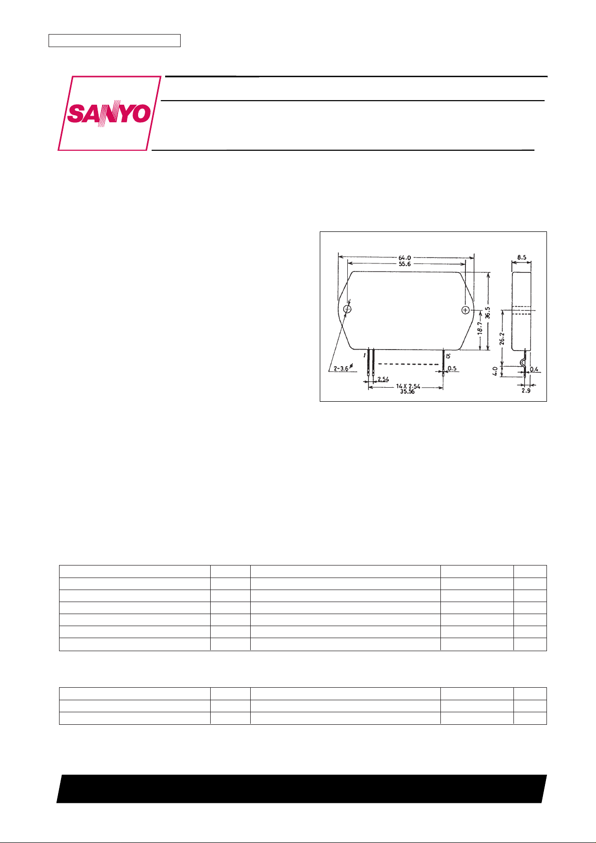
Package Dimensions
unit : mm
4075
Specifications
Maximum Ratings at Ta = 25°C
Recommended Operational Voltage at Ta = 25°C
[STK4042V]
Parameter Symbol Conditions Ratings Unit
Maximum supply voltage V
CC
max ±65 V
Thermal resistance
θj-c 1.2 °C/W
Junction temperature Tj 150 °C
Operating substrate temperature Tc 125 °C
Storage temperature Tstg –30 to +125 °C
Available time for load shorted ts *1V
CC
= ±45 V, RL= 8 Ω, f = 50 Hz, PO= 80 W 1 s
Parameter Symbol Conditions Ratings Unit
Recommended supply voltage V
CC
±45 V
Load resistance R
L
8 Ω
STK4042V
No. 4390-2/5
Operating Characteristics
at Ta = 25°C, VCC= ±45 V, RL= 8 Ω, VG = 40 dB, Rg = 600 Ω, 100k LPF ON, RL(non-inductive)
Note: Use rated power supply for test unless otherwise specified.
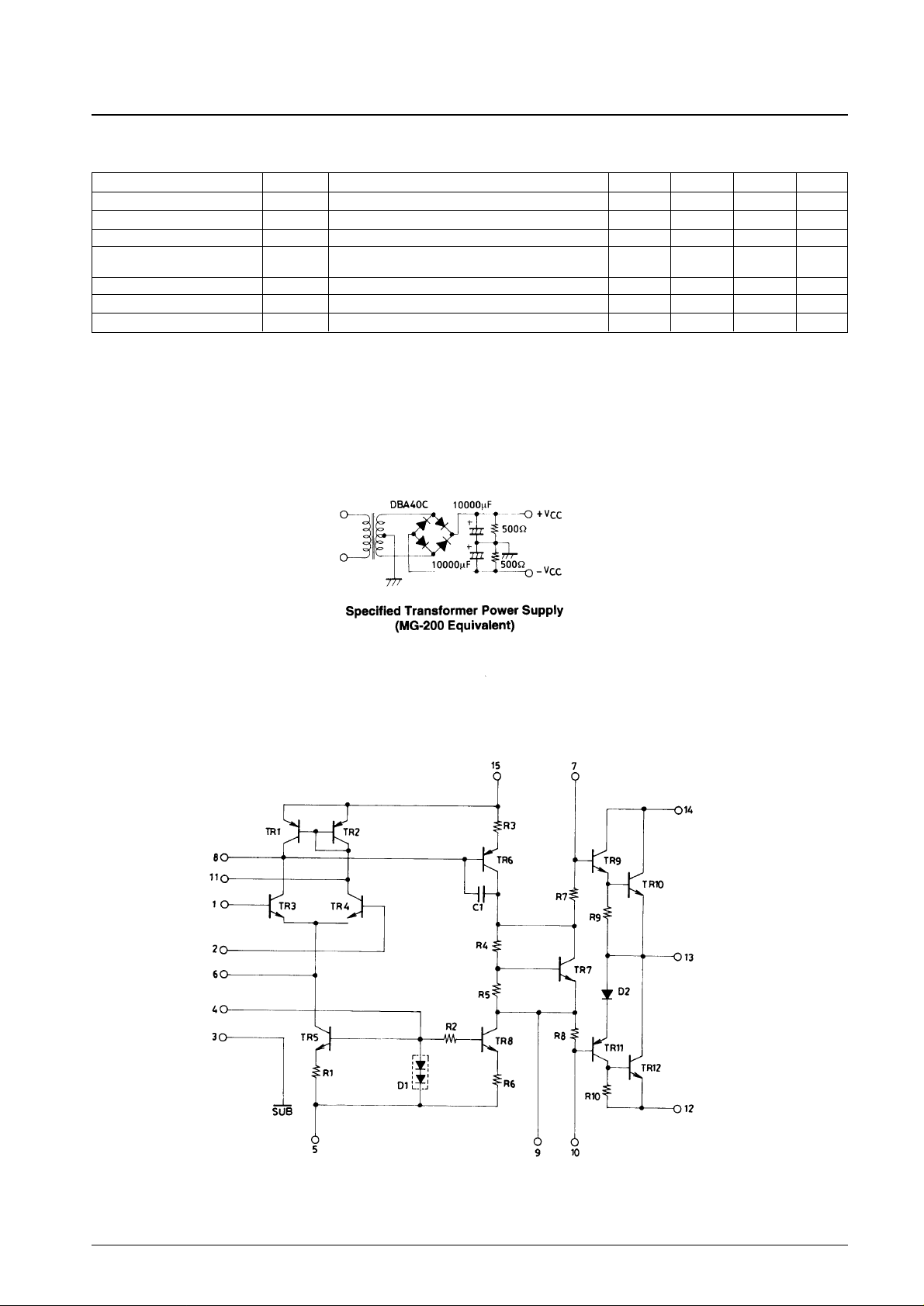
*1 When measuring permissible load short time and output noise voltage use transformer power supply indicated below.
*2 Output noise voltage represents the peak value on the rms scale (VTVM). The noise voltage waveform does not include the pulse noise.
Equivalent Circuit
Parameter Symbol Conditions min typ max Unit
Quiescent current I
CCO
V
CC
= ±54 V 15 120 mA
Output power P
O
(1) THD = 0.08%, f = 20 Hz to 20 kHz 80 W
Total harmonic distortion THD P
O
= 1.0 W, f = 1 kHz 0.08 %
Frequency response f
L
, f
H
PO = 1.0 W,
+0
dB 20 to 50k Hz
–3
Input resistance r
i
PO = 1.0 W, f = 1 kHz 55 kΩ
Output noise voltage V
NO
*2 V
CC
= ±54 V, Rg=10 kΩ 1.2 mVrms
Neutral voltage V
N
V
CC
= ±54 V –70 0 +70 mV
 Loading...