

SANYO STK401-060 Datasheet
↓
Ordering number: EN 4680B
Thick Film Hybrid IC
STK401-060
AF Power Amplifier (Split Power Supply)
(35W + 35W min, THD = 0.4%)
Overview
The STK401-060 is a thick-film audio power amplifier IC
belonging to a series in which all devices are pin compatible. This allows a single PCB design to be used to construct amplifiers of various output capacity simply by
changing hybrid ICs. Also, this series is part of a new,
larger series that comprises mutually similar devices with
the same pin compatibility. This makes possible the development of a 2-channel amplifier from a 3-channel amplifier using the same PCB. In addition, this new series
features 6/3 Ω drive in order to support the low impedance
of modern speakers.
Features
• Pin compatible
STK400-000 series (3-channel/single package)
STK401-000 series (2-channel/single package)
• Output load impedance R
• New pin configuration
Pin configuration has been grouped into individual
blocks of inputs, outputs and supply lines, minimizing
the adverse effects of pattern layout on operating characteristics.
• Few external components
In comparison with existing series, external bootstrap
resistors and capacitors can be eliminated.
= 6/3 Ω supported
L
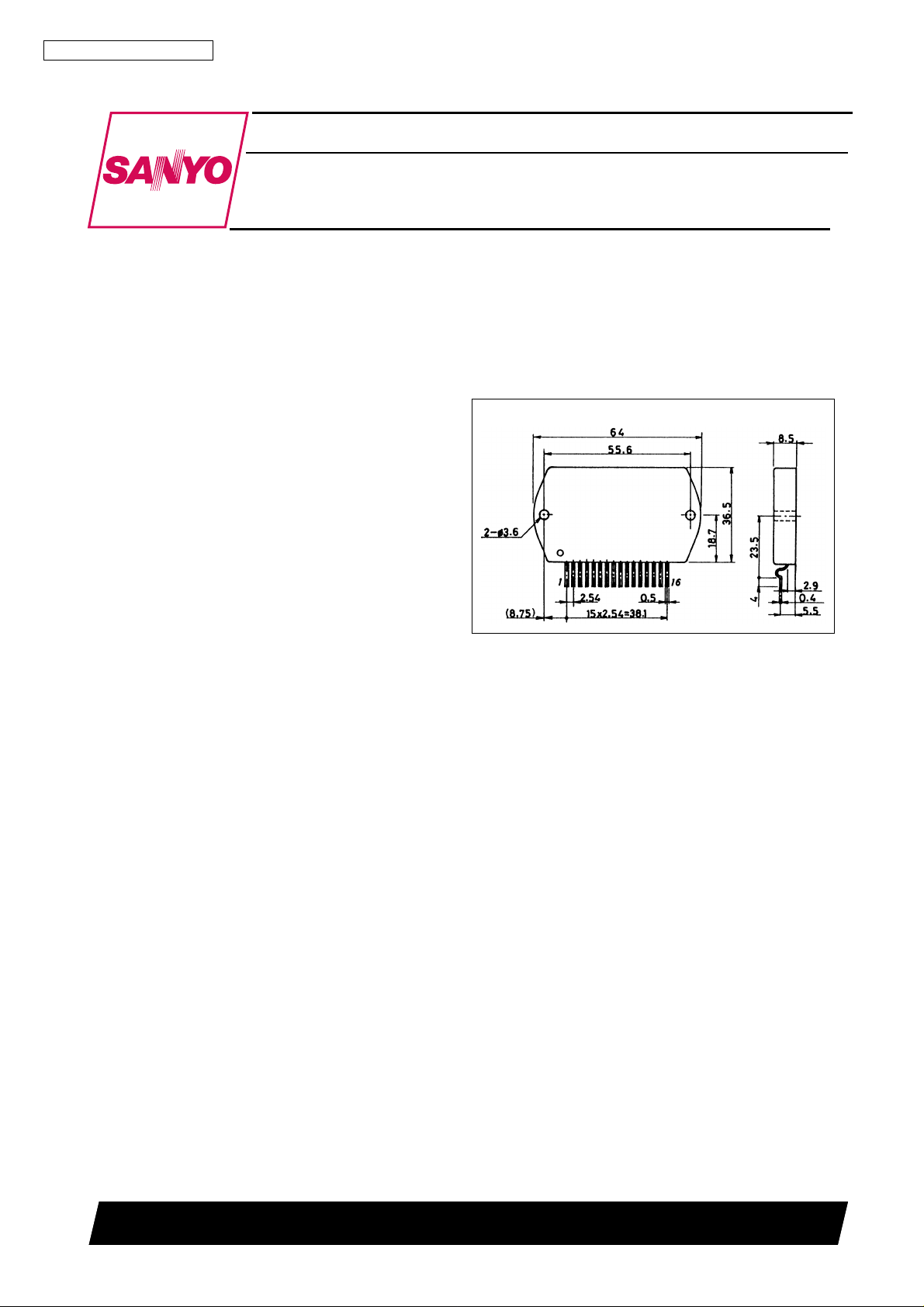
Package Dimensions
unit: mm
4134
[STK401-060]
SANYO Electric Co., Ltd. Semiconductor Business Headquarters
TOKYO OFFICE Tokyo Bldg., 1-10, 1 Chome, Ueno, Taito-ku, TOKYO, 110 JAPAN
10997HA(ID) / 71696HA(ID) / 41495TH(ID) No. 4680—1/8
Specifications
±
θ
°
°
°
−
°
−
STK401-060
Maximum Ratings
at Ta = 25 ° C
Parameter Symbol Conditions Ratings Unit
Maximum supply voltage
Thermal resistance
V
max
CC
j-c Per power transistor 1.8
Junction temperature Tj 150
Operating substrate temperature Tc 125
Storage temperature Tstg
Available time for load short-circuit t
Operating Characteristics
at Ta = 25 ° C, R
V
= ± 28V, R
s
CC
f = 50Hz, P
= 6 Ω (noninductive load), Rg = 600 Ω , VG = 40dB
L
= 6 Ω ,
L
= 35W
O
30 to +125
Parameter Symbol Conditions min typ max Unit
Quiescent current I
P
Output power
P
THD(1)
Total harmonic distortion
THD(2)
Frequency response f
Input impedance r
Output noise voltage V
Neutral voltage V
CCO
(1)
O
(2)
O
, f
L
i
NO
N
H
V
= ± 34V 20 60 100 mA
CC
V
= ± 28V, f = 20Hz to
CC
20kHz, THD = 0.4%
V
= ± 23V, f = 1kHz,
CC
THD = 1.0%, R
V
= ± 28V, f = 20Hz to
CC
20kHz, P
V
= ± 28V, f = 1kHz,
CC
P
= 5.0W
O
V
= ± 28V, P
CC
V
= ± 28V, f = 1kHz,
CC
P
= 1.0W
O
V
= ± 34V, Rg = 10k Ω
CC
V
= ± 34V
CC
= 3 Ω
L
= 1.0W
O
= 1.0W, – 20 to 50k – Hz
O
+0
dB
−
3
35 40 – W
35 40 – W
– – 0.4 %
– 0.01 – %
–55–k
– – 1.2 mVrms
70 0 +70 mV
41 V
C/W
C
C
C
1s
Ω
Notes.
All tests are measured using a constant-voltage supply unless otherwise specified.
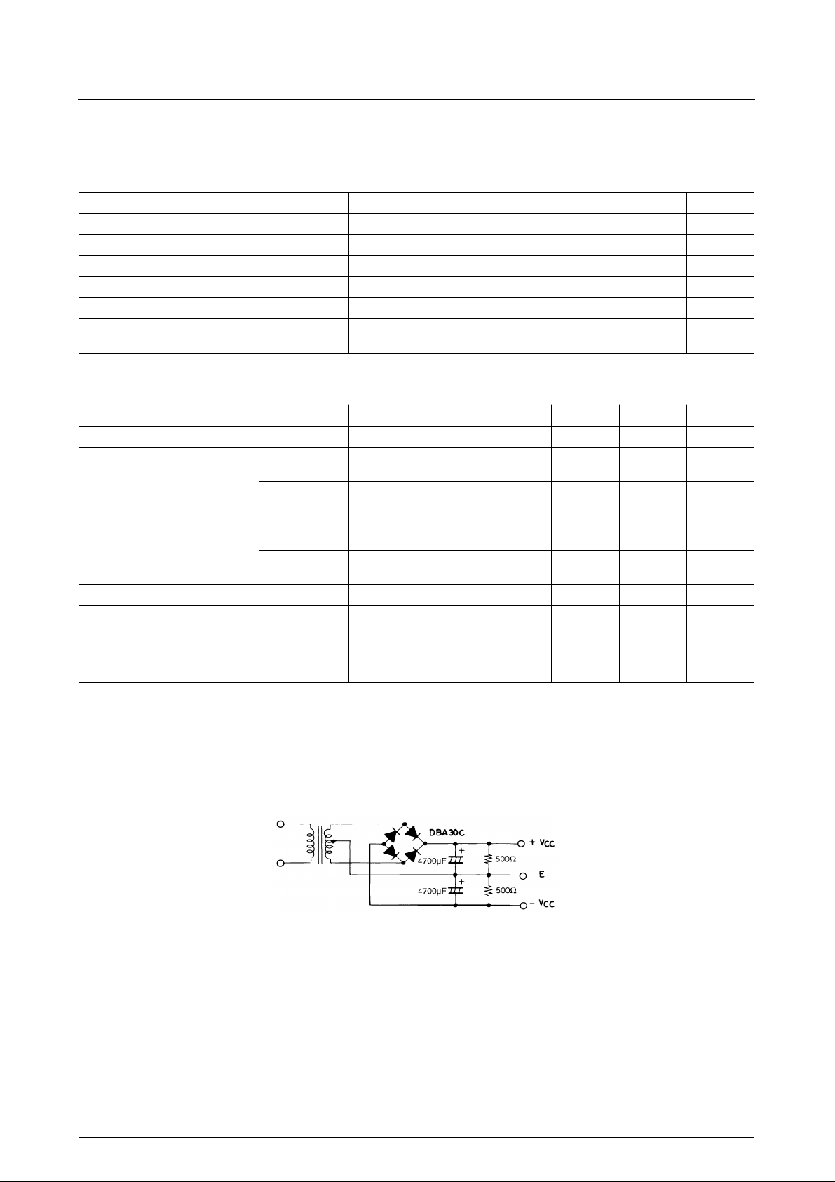
Available time for load short-circuit and output noise voltage are measured using the transformer supply specified below.
The output noise voltage is the peak value of an av er age-reading meter with an rms value scale (VTVM). A regulated AC supply (50Hz) should be used to eliminate the
effects of AC primary line flicker noise.
Specified Transformer Supply (RP-25 or Equivalent)
No. 4680—2/8
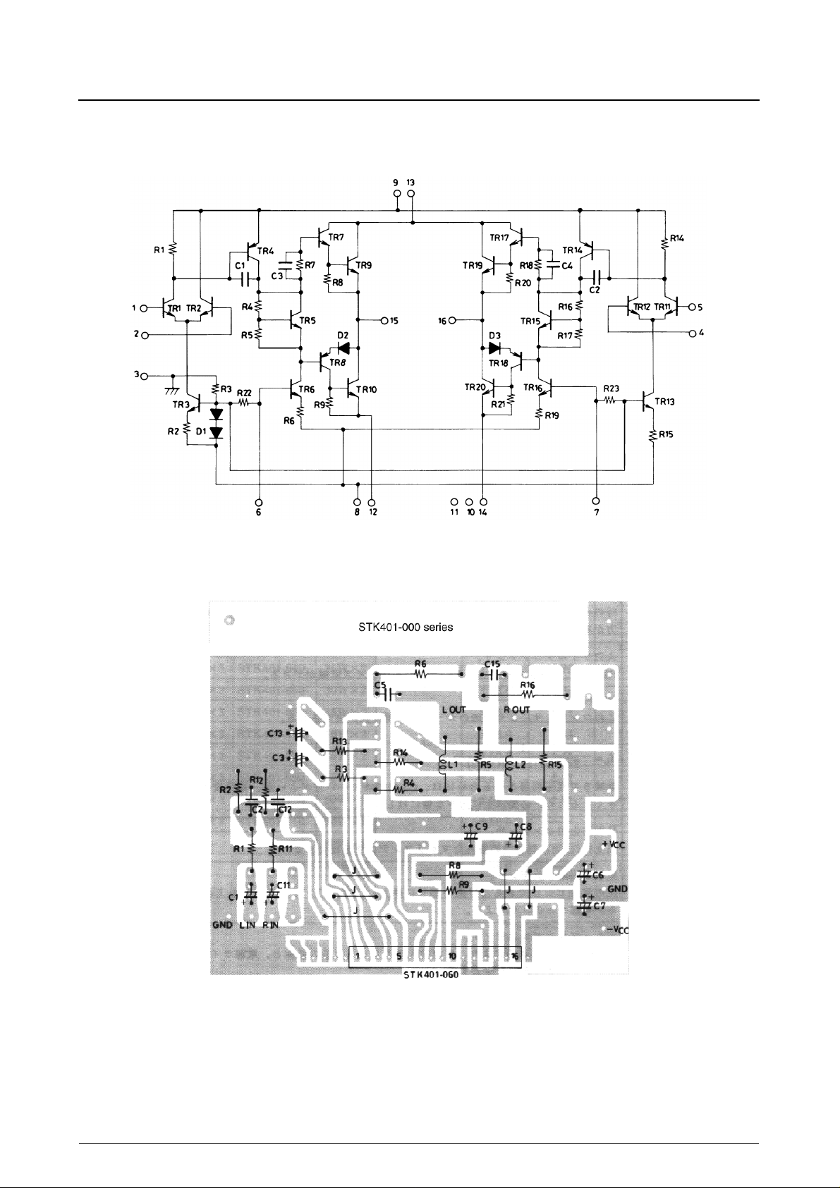
Equivalent Circuit
STK401-060
Sample PCB Layout for 2-Channel or 3-Channel Amplifiers
Pin 6 of STK400-000 series devices corresponds to pin 1 of STK401-000 series devices.
Copper (Cu) foil surface
No. 4680—3/8
 Loading...