

SANYO STK401-020 Datasheet
Overview
Now, thick-film audio power amplifier ICs are available
with pin-compatibility to permit a single PCB to be
designed and amplifier output capacity changed simply by
installing a hybrid IC. This new series was developed
with this kind of pin-compatibility to ensure integration
between systems everywhere. With this new series of IC,
even changes from 3-channel amplifier to 2-channel
amplifiers is possible using the same PCB. In addition,
this new series of ICs has a 6/3Ω drive in order to support
the low impedance of modern speakers.
Features
• Pin-compatible
STK400-000 series (3-channel/single package)
STK401-000 series (2-channel/single package)
• Output load impedance RL=6Ω/3Ω supported
• New pin arrangement
To simplify input/output pattern layout and minimize
the effects of pattern layout on operational
characteristics, pin assignments are grouped into blocks
consisting of input, output and power systems.
• Few external circuits
Compared to those series used until now, boot-strap
capacitors and boot-strap resistors for external circuits
can be greatly reduced.
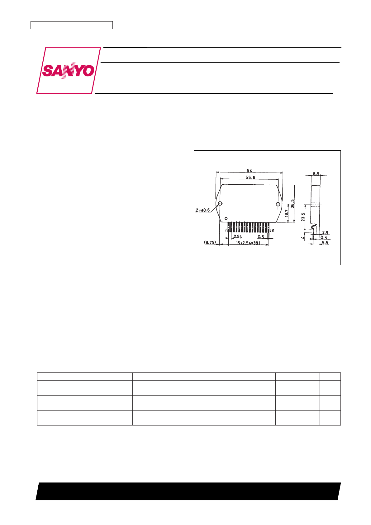
Package Dimensions
unit: mm
4134
Thick-Film Hybrid IC
N3096HA(OT)/31293YO 5-3211 No. 4341-1/9
[STK401-020]
SANYO Electric Co.,Ltd. Semiconductor Bussiness Headquarters
TOKYO OFFICE Tokyo Bldg., 1-10, 1 Chome, Ueno, Taito-ku, TOKYO, 110 JAPAN
AF Power Amplifier (Split Power Supply)
(15 W + 15 W min, THD = 0.4%)
STK401-020
Ordering number : EN4341A
Parameter Symbol Conditions Ratings Unit
Maximum supply voltage V
CC
max ±29 V
Thermal resistance
θj-c Per power transistor 2.1 °C/W
Junction temperature Tj 150 °C
Operating substrate temperature Tc 125 °C
Storage temperature range Tstg –30 to +125 °C
Permissible load short time t
s
VCC= ±20 V, RL= 6 Ω, f = 50 Hz, Po= 15 W 1 s
Specifications
Maximum Ratings at Ta = 25°C
➙
Operating Characteristics at Ta = 25°C, RL= 6 Ω, Rg = 600 Ω, VG = 40dB, RL(non-inductive)
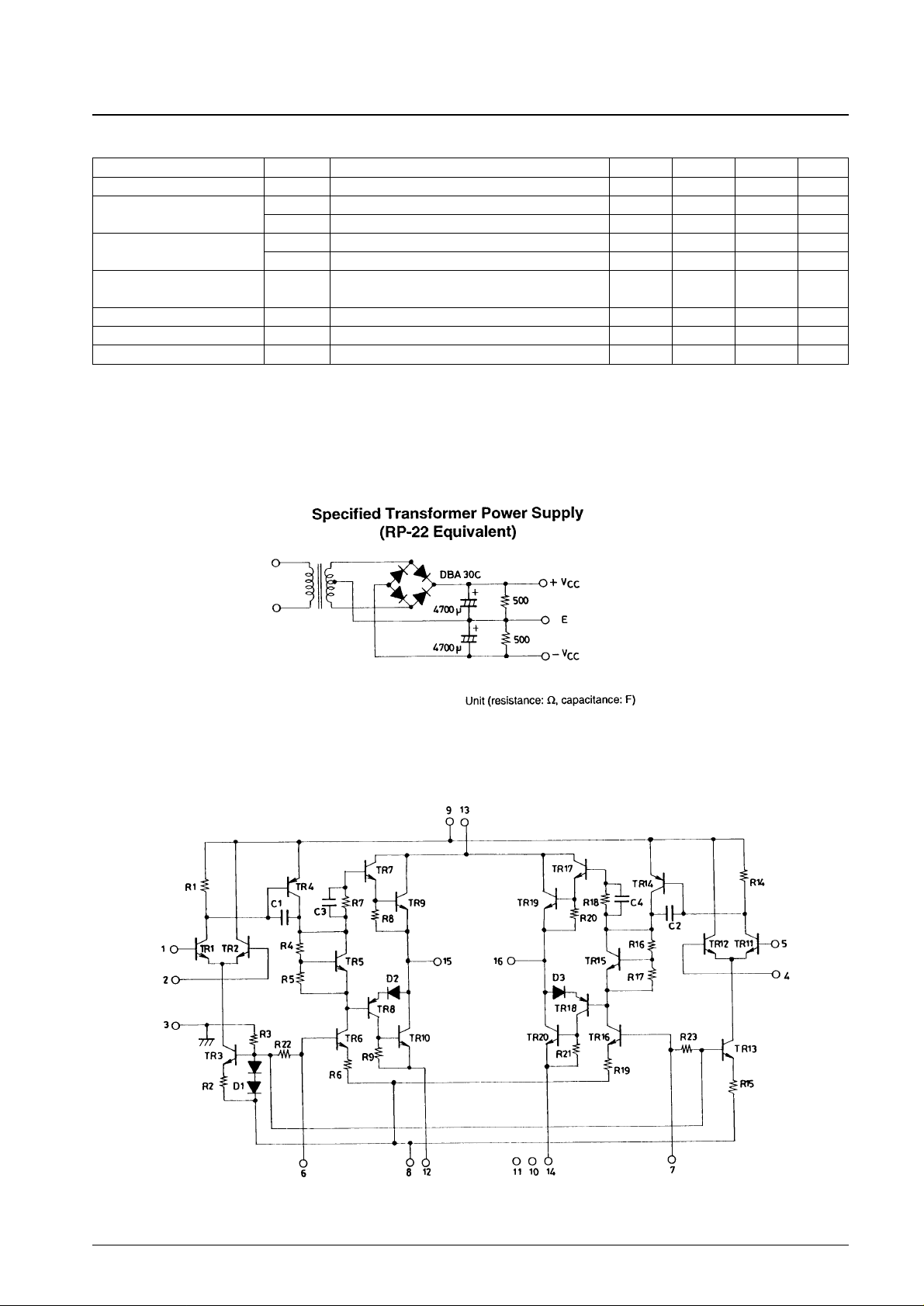
Internal Equivalent Circuit
Notes
• Use rated power supply for test unless otherwise specified.
• When measuring permissible load short time and output noise voltage use transformer power supply indicated below.
• Output noise voltage is represented by the peak value rms (VTVM) for mean reading. Use an AC stabilized power
supply (50 Hz) on the primary side to eliminate the effect of AC flicker noise.
No. 4341-2/9
STK401-020
Parameter Symbol Conditions min typ max Unit
Quiescent current I
CCO
V
CC
± 24 V 20 60 100 mA
Output power
Po (1) V
CC
± 20 V, f = 20 to 20 kHz, THD = 0.4% 15 20 W
Po (2) V
CC
± 16 V, f = 1 kHz, THD = 1.0%, RL= 3 Ω 15 20 W
Total harmonic distortion
THD (1) V
CC
± 20 V, f = 20 to 20 kHz, PO= 1.0 W 0.4 %
THD (2) V
CC
± 20 V, f = 1 kHz, PO= 5.0 W 0.02 %
+0
Frequency response f
L
, f
H
V
CC
± 20 V, PO= 1.0 W,
–3
dB 20 to 50 k Hz
Input impedance r
i
V
CC
± 20 V, f = 1 kHz, PO= 1.0 W 55 kΩ
Output noise voltage V
NO
V
CC
± 24 V, Rg = 10 kΩ 1.2 mVrms
Neutral voltage V
N
V
CC
± 24 V –70 0 70 mV
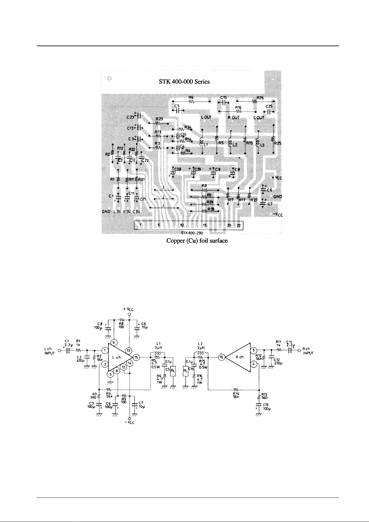
Pattern Example for PCB used with either 2- or 3-channel Amplifiers.
Sample Application Circuit
Unit (resistance: Ω, capacitance: F)
With the STK401-000 series, the 6 pin corresponds to the 1 pin with respect to the
STK400-000 series.
No. 4341-3/9
STK401-020
 Loading...