

Page 1
Any and all SANYO products described or contained herein do not have specifications that can handle
applications that require extremely high levels of reliability, such as life-support systems, aircraft’s
control systems, or other applications whose failure can be reasonably expected to result in serious
physical and/or material damage. Consult with your SANYO representative nearest you before using
any SANYO products described or contained herein in such applications.
SANYO assumes no responsibility for equipment failures that result from using products at values that
exceed, even momentarily, rated values (such as maximum ratings, operating condition ranges,or other
parameters) listed in products specifications of any and all SANYO products described or contained
herein.
Thick Film Hybrid IC
3-Channel Convergence Correction Circuit
(I
C
max = 3A)
Ordering number:ENN5170
STK392-110
SANYO Electric Co.,Ltd. Semiconductor Company
TOKYO OFFICE Tokyo Bldg., 1-10, 1 Chome, Ueno, Taito-ku, TOKYO, 110-8534 JAPAN
Overview
The STK392-110 is a conver gence correction circuit IC for
video projectors. It incorporates three output amplifiers in
a single package, making possible the construction of CR T
horizontal and vertical convergence correction output circuits for each of the RGB colors using ust two hybrid ICs.
The output circuit use a class-B configuration, in comparison with the STK392-010, realizing a more compact package and lower cost.
Applications
• V ideo projectors
Features
• 3 output amplifier circuits in a single package
• High maximum supply voltage (VCC max = ±38V)
• Low thermal resistance (θj-c=3.0°C/W)
• High temperature stability (TC max=125°C)
• Separate predriver and output stage supplies
• Output stage supply switching for high-performance
designs
• Low inrush current when power is applied
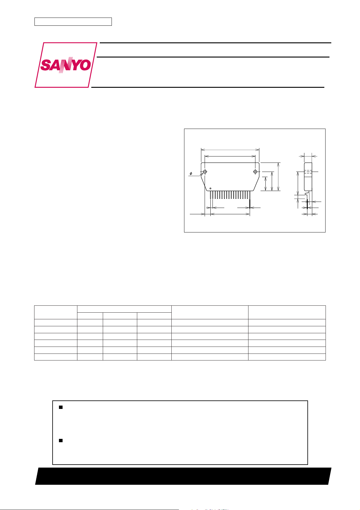
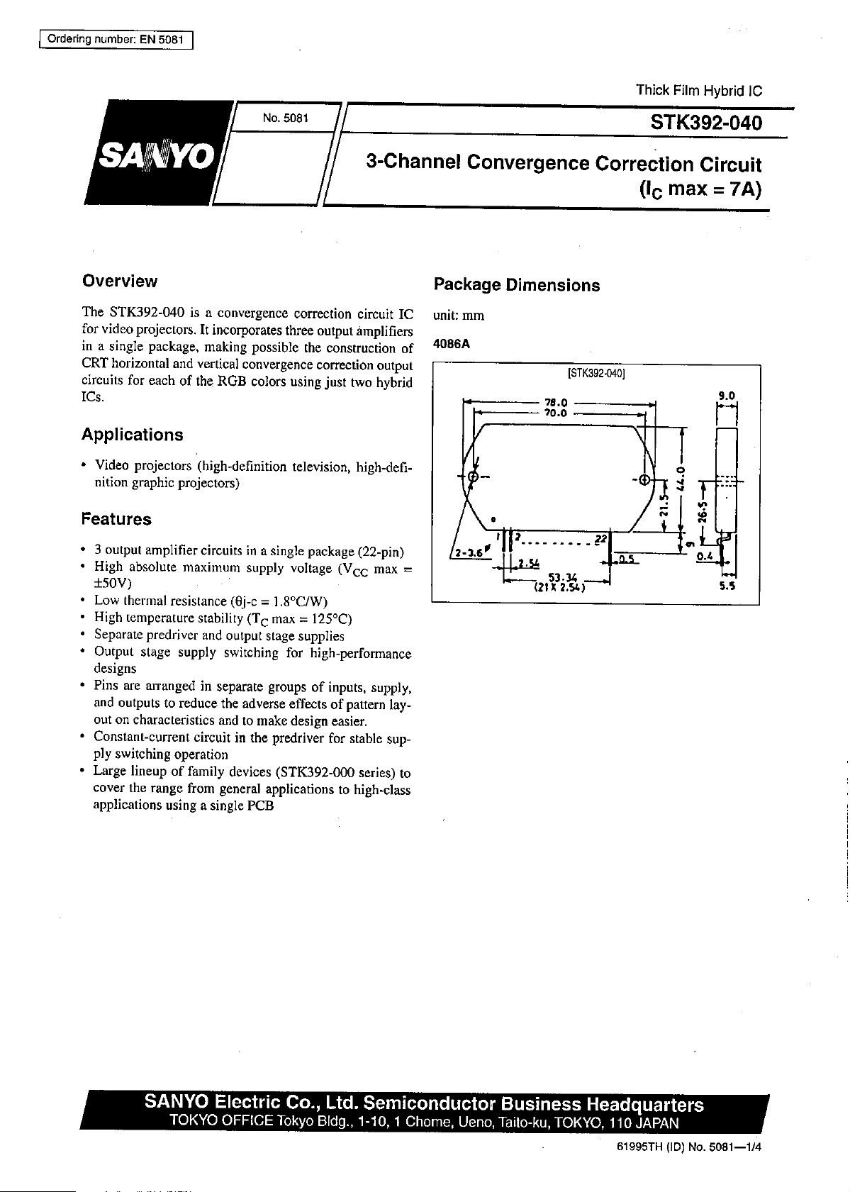
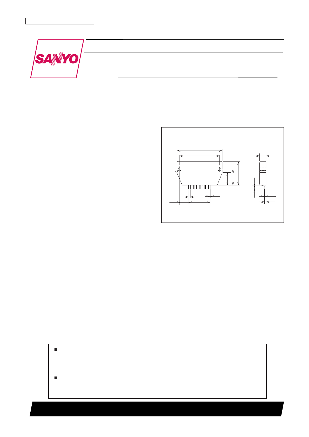
Package Dimensions
unit:mm
4083
3.6
118
(6.21)
64.0
55.6
2.54
17×2.54=43.18
[STK392-110]
16.5
0.5
21.0
31.0
8.5
25.8
4.0
5.5
SANYO : SIP18
2.9
0.4
Series Organization
The following devices form a series with varying output capacity and application grade. Some of the devices below are
under development, so contact your nearest sales representative for details.
.oNepyT
V
xamICxam
011-293KTSV83±A3zHk51sVTnoitcejorplareneG
010-293KTSV83±A5zHk51sVTnoitcejorplareneG
020-293KTSV44±A6zHk53AGV,DH
040-293KTSV05±A7zHk001MAC,DAC,AGX
012-293KTSV56±A8zHk031MAC,DAC
022-293KTSV57±A01zHk061MAC,DAC
CC
sgnitarmumixaM
θ c-j
3.0˚C/W
2.6˚C/W
2.1˚C/W
1.8˚C/W
1.5˚C/W
1.3˚C/W
fHxam
ycneuqerflatnozirohmumixaM
93099TH (KT)/80995HA (ID) No.5170–1/4
edargnoitacilppA
Page 2
STK392-1 10
Specifications
Maximum Ratings at Ta = 25˚C
retemaraPlobmySsnoitidnoCsgnitaRtinU
egatlovylppusmumixaMV
tnerrucrotcellocmumixaMI
ecnatsiserlamrehT
erutarepmetnoitcnuJjT 051
erutarepmetgnitarepOcT 521
erutarepmetegarotSgtsT 521+ot03–
Operating Characteristics at Ta = 25˚C, Rg=50Ω, VCC=±30V, specified test circuit
retemaraPlobmySsnoitidnoC
egatlovesiontuptuOV
tnerructnecseiuQI
egatlovlartueNV
emityaledtuptuOt
Note :
All tests are conducted using a constant-voltage regulated supply unless otherwise specified.
The output noise voltage is the peak value of an average-reading meter with an rms value scale (VTVM).
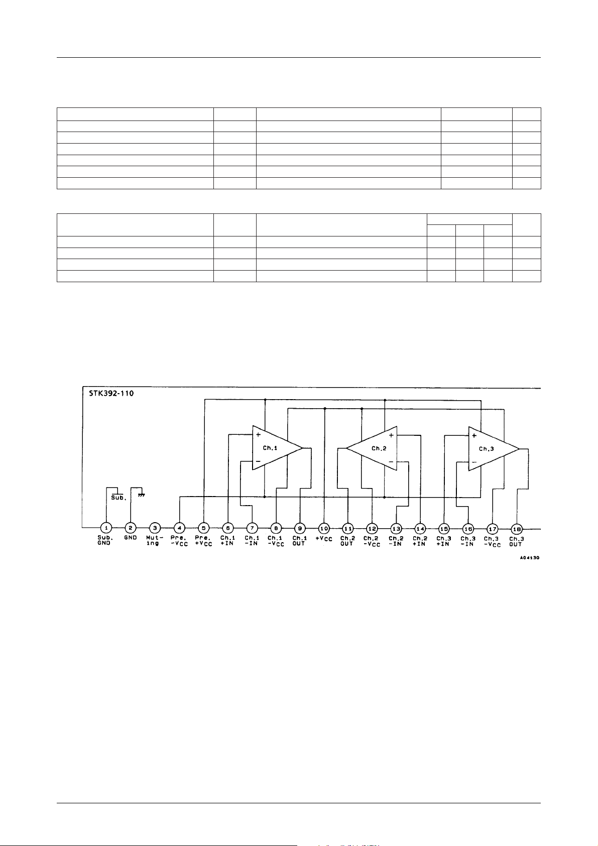
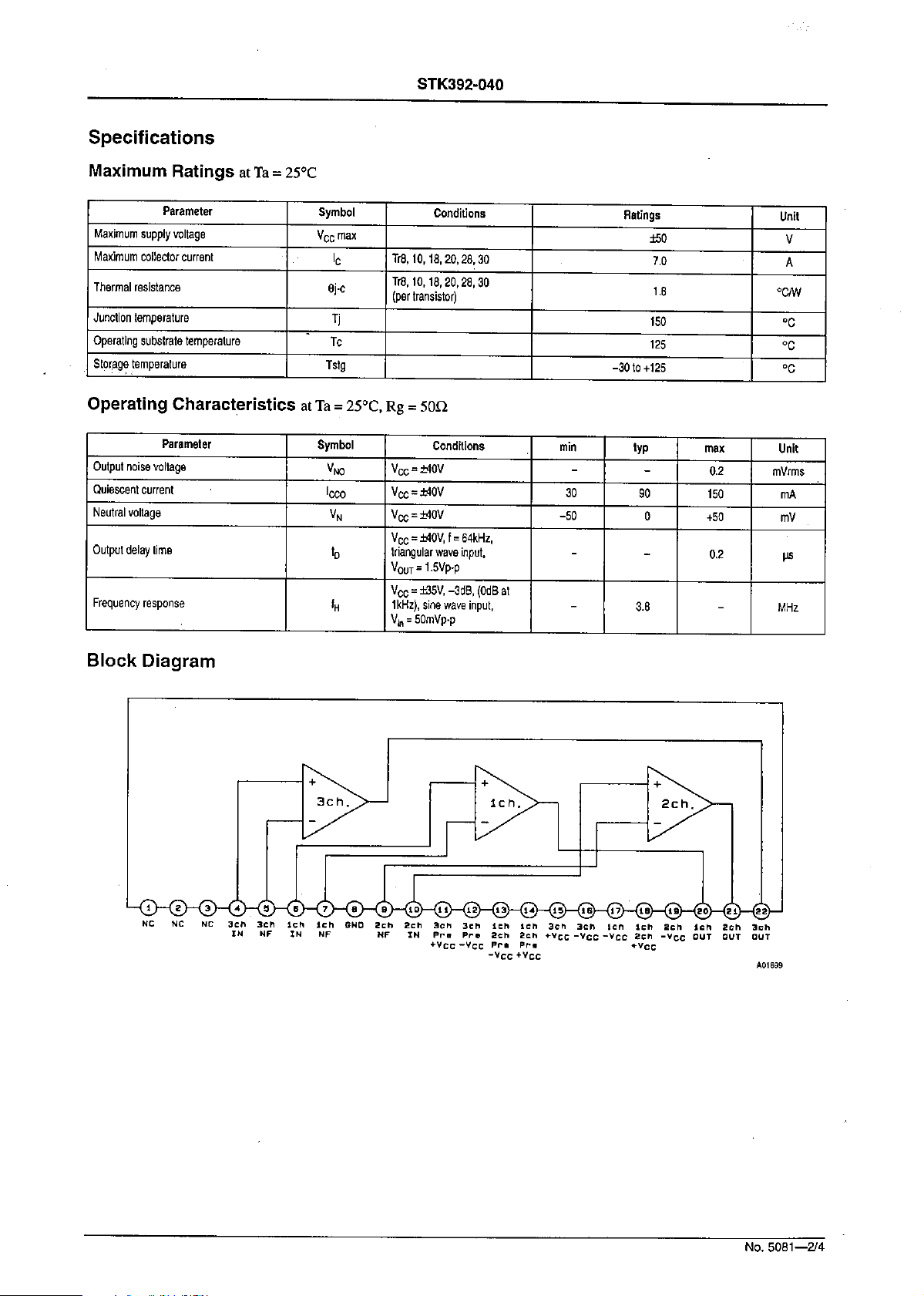
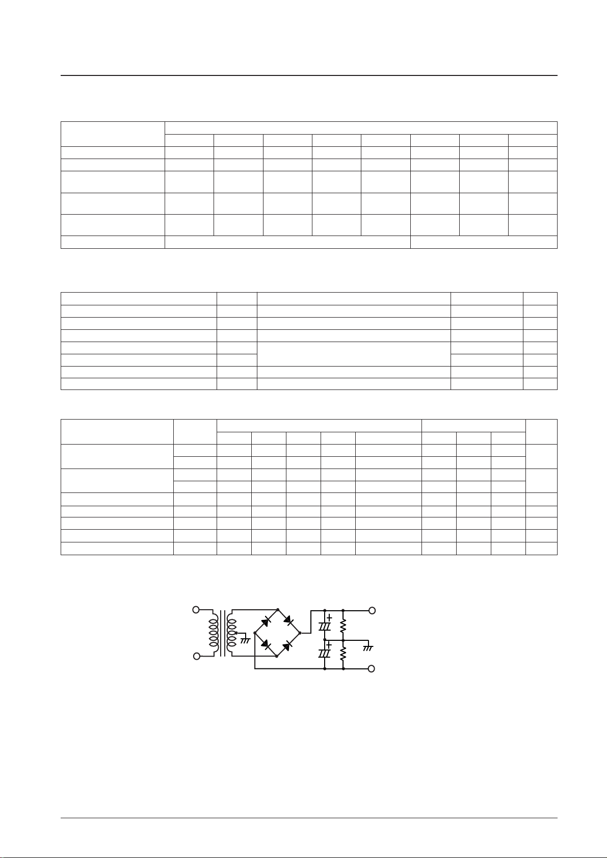
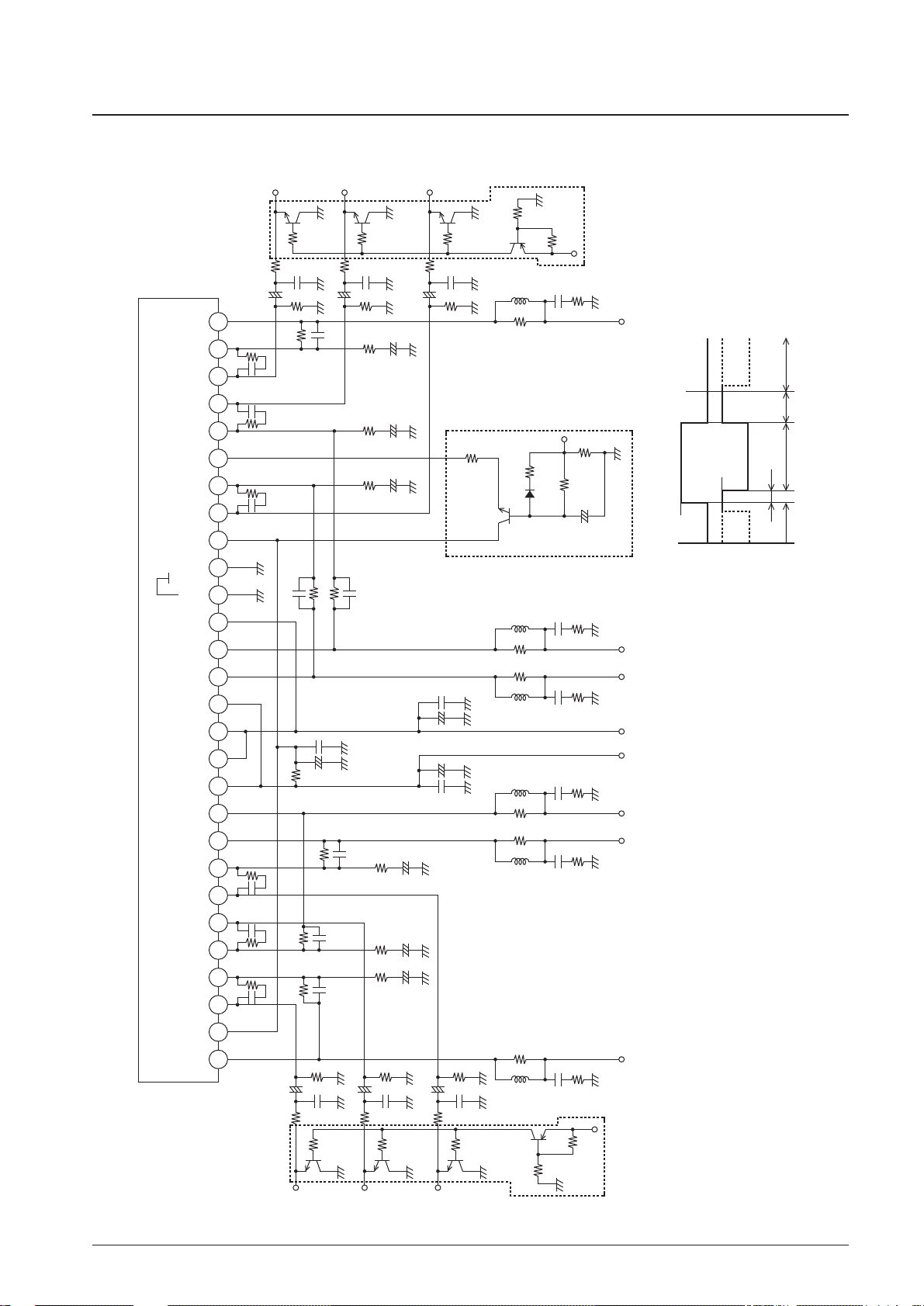
Block Diagram
xam 83±V
CC
C
θ c-j
ON
OCC
N
D
12,02,41,31,7,6rT 0.3A
)rotsisnartrep(12,02,41,31,7,6rT 0.3
V,tupnievawralugnairt,zHk57.51=f
TUO
˚C/W
sgnitaR
nimpytxam
2.0smrVm
512203Am
05–005+Vm
p-pV5.1=1sµ
˚C
˚C
˚C
tinU
No.5170–2/4
Page 3
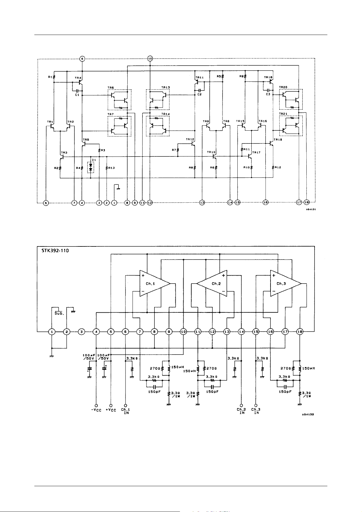
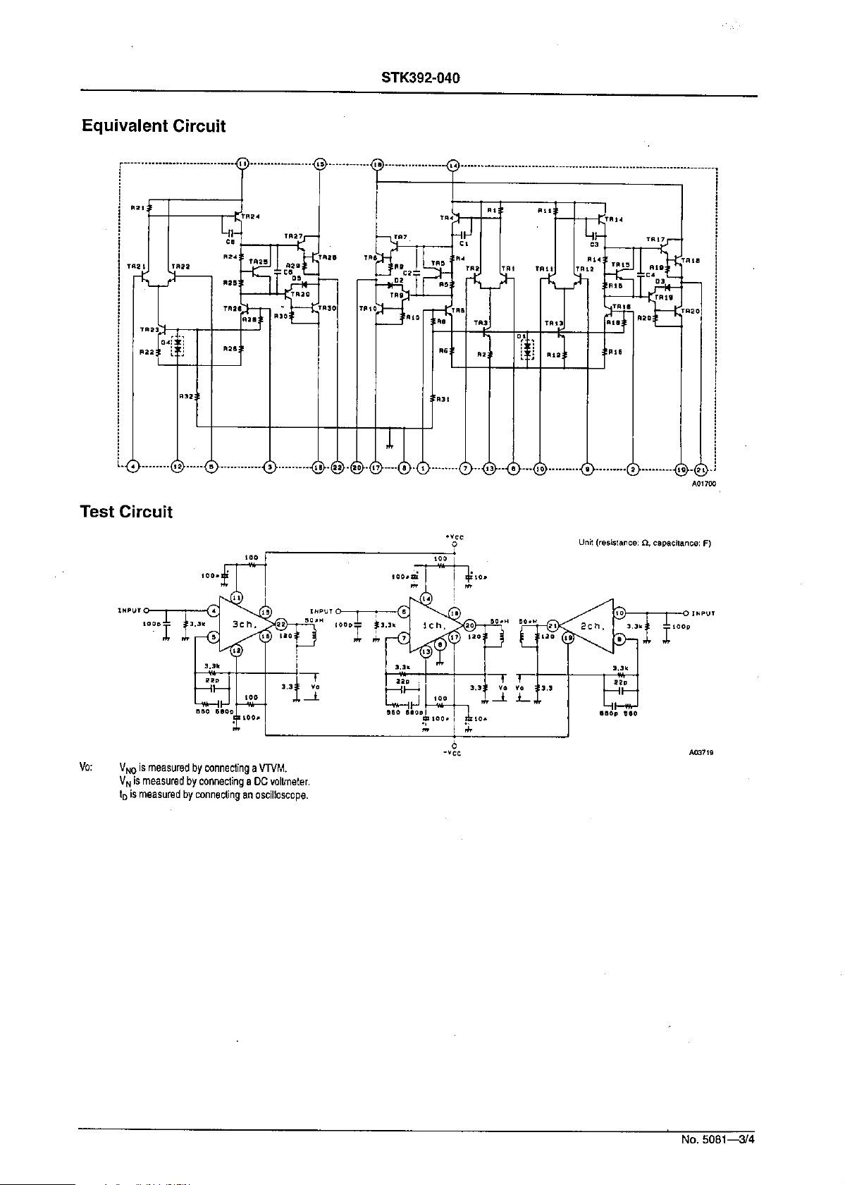
Equivalent Circuit
STK392-1 10
Test Circuit
No.5170–3/4
Page 4
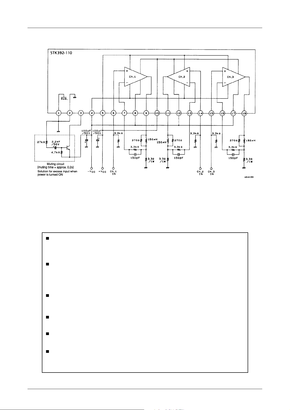
Sample Application Circuit
STK392-1 10
Specifications of any and all SANYO products described or contained herein stipulate the performance,
characteristics, and functions of the described products in the independent state, and are not guarantees
of the performance, characteristics, and functions of the described products as mounted in the customer's
products or equipment. To verify symptoms and states that cannot be evaluated in an independent device,
the customer should always evaluate and test devices mounted in the customer's products or equipment.
SANYO Electric Co., Ltd. strives to supply high-quality high-reliability products. However, any and all
semiconductor products fail with some probability. It is possible that these probabilistic failures could
give rise to accidents or events that could endanger human lives, that could give rise to smoke or fire,
or that could cause damage to other property. When designing equipment, adopt safety measures so
that these kinds of accidents or events cannot occur. Such measures include but are not limited to protective
circuits and error prevention circuits for safe design, redundant design, and structural design.
In the event that any or all SANYO products(including technical data,services) described or
contained herein are controlled under any of applicable local export control laws and regulations,
such products must not be exported without obtaining the export license from the authorities
concerned in accordance with the above law.
No part of this publication may be reproduced or transmitted in any form or by any means, electronic or
mechanical, including photocopying and recording, or any information storage or retrieval system,
or otherwise, without the prior written permission of SANYO Electric Co. , Ltd.
Any and all information described or contained herein are subject to change without notice due to
product/technology improvement, etc. When designing equipment, refer to the "Delivery Specification"
for the SANYO product that you intend to use.
Information (including circuit diagrams and circuit parameters) herein is for example only ; it is not
guaranteed for volume production. SANYO believes information herein is accurate and reliable, but
no guarantees are made or implied regarding its use or any infringements of intellectual property rights
or other rights of third parties.
This catalog provides information as of September, 1999. Specifications and information herein are
subject to change without notice.
PS No.5170–4/4
Page 5
Page 6
Page 7
Page 8
Page 9
Ordering number : ENN7065A
D0102AS (OT) No. 7065-1/5
Overview
The STK402-000 series products are audio power
amplifier hybrid ICs that consist of optimally-designed
discrete component power amplifier circuits that have
been miniaturized using SANYO's unique insulated metal
substrate technology (IMST). SANYO has adopted a new
low thermal resistance substrate in these products to
reduce the package size by about 60% as compared to the
earlier SANYO STK407-000 series.
Features
• Series of pin compatible power amplifiers ranging from
20 W × 2 channels to 120 W × 2 channels (10%/1 kHz)
devices. The same printed circuit board can be used
depending on the output power grade.
• The pin arrangement is compatible with that of the 3channel STK402-200 series. This means that 3-channel
printed circuit boards can also be used for 2-channel
products.
• Miniature packages
— 15 W/ch to 40 W/ch (THD = 0.4%, f = 20 Hz to
20 kHz); 46.6 mm × 25.5 mm ×8.5 mm *
— 50 W/ch to 80 W/ch (THD = 0.4%, f = 20 Hz to
20 kHz); 59.2 mm × 31.0 mm × 8.5 mm *
*: Not including the pins.
• Output load impedance: RL= 6 Ω
• Allowable load shorted time: 0.3 seconds
• Supports the use of standby, muting, and load shorting
protection circuits.
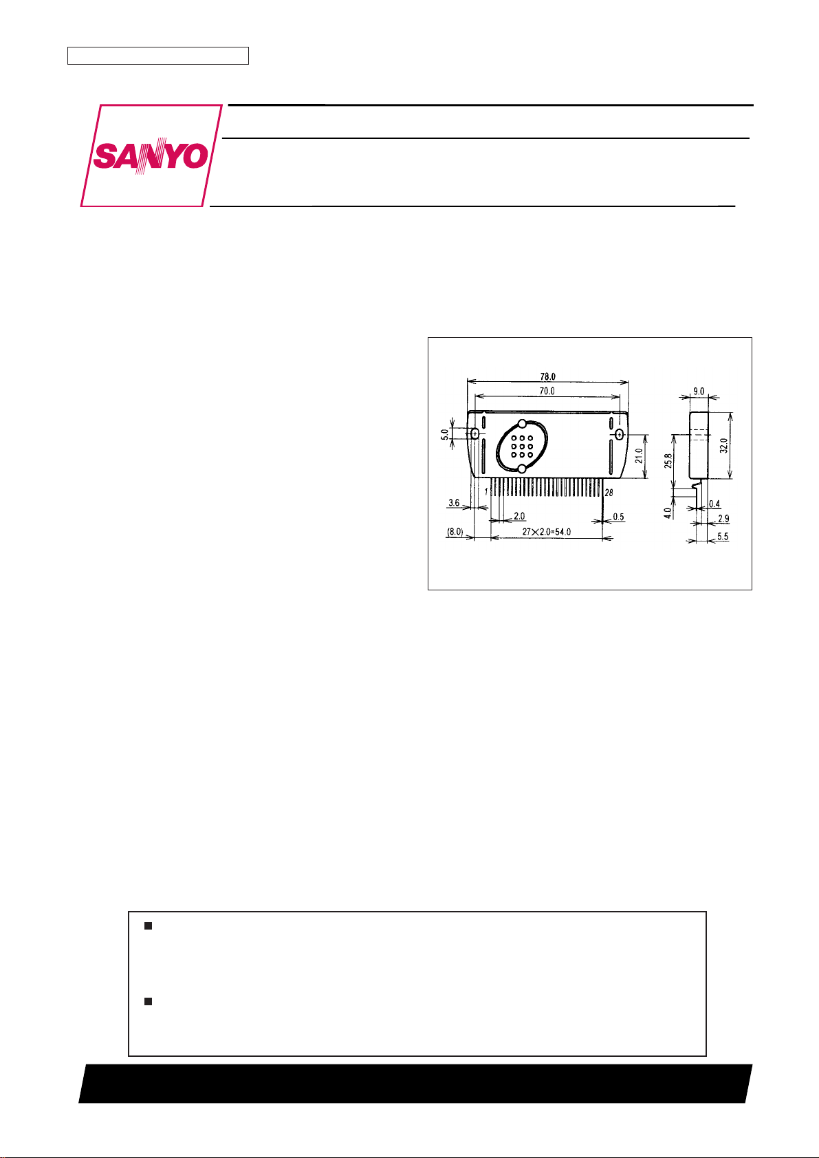
Package Dimensions
unit: mm
4190-SIP15
59.2
52.0
(12)
ø3.6
2.0
14X2=28
0.5
15
8.5
0.4
2.9
16.5
21.0
4.0 1.0
31.0
1
SANYO: SIP15
[STK402-090]
STK402-090
SANYO Electric Co.,Ltd. Semiconductor Company
TOKYO OFFICE Tokyo Bldg., 1-10, 1 Chome, Ueno, Taito-ku, TOKYO, 110-8534 JAPAN
Two-Channel Class AB Audio Power Amplifier IC
50 W + 50 W
Thick-Film Hybrid IC
Any and all SANYO products described or contained herein do not have specifications that can handle
applications that require extremely high levels of reliability, such as life-support systems, aircraft’s
control systems, or other applications whose failure can be reasonably expected to result in serious
physical and/or material damage. Consult with your SANYO representative nearest you before using
any SANYO products described or contained herein in such applications.
SANYO assumes no responsibility for equipment failures that result from using products at values that
exceed, even momentarily, rated values (such as maximum ratings, operating condition ranges, or other
parameters) listed in products specifications of any and all SANYO products described or contained
herein.
Page 10
No. 7065-2/5
STK402-090
Item
Type No.
STK402-020 STK402-030 STK402-040 STK402-050 STK402-070 STK402-090 STK402-100 STK402-120
Output 1 (10%/1 kHz) 20 W + 20 W 30 W + 30 W 40 W + 40 W 45 W +45 W 60 W + 60 W 80 W + 80 W
100 W + 100 W120 W + 120 W
Output 2 (0.4%/20 Hz to 20 kHz)
15 W + 15 W 20 W + 20 W 25 W + 25 W 30 W + 30 W 40 W + 40 W 50 W + 50 W 60 W + 60 W 80 W + 80 W
Maximum supply voltage
±30 V ±34 V ±38 V ±40 V ±50 V ±54 V ±57 V ±65 V
(No signal)
Maximum supply voltage
±28 V ±32 V ±36 V ±38 V ±44 V ±47 V ±50 V ±57 V
(6 Ω)
Recommended supply voltage
±19 V ±22 V ±25 V ±26.5 V ±30 V ±32 V ±35 V ±39 V
(6 Ω)
Package 46.6 mm × 25.5 mm × 8.5 mm 59.2 mm × 31.0 mm × 8.5 mm
Series Organization
Parameter Symbol Conditions Ratings Unit
Maximum supply voltage (No signal) V
CC
max(0) ±54 V
Maximum supply voltage V
CC
max(1) RL= 6 Ω ±47 V
Thermal resistance θj-c Per power transistor 2.2 °C/W
Junction temperature Tj max
Both the Tj max and the Tc max conditions must be met.
150 °C
Operating IC substrate temperature Tc max 125 °C
Storage temperature Tstg –30 to +125 °C
Allowable load shorted time *
2
ts VCC= ±32.0 V, RL= 6 Ω, f = 50 Hz, PO= 50 W 0.3 s
Specifications
Maximum Ratings at Ta = 25°C
These products are organized as a series based on their output capacity.
Parameter Symbol
Conditions*
1
Ratings
Unit
V
CC
(V) f (Hz) PO(W) THD (%) min typ max
Output power
P
O
(1) ±32.0 20 to 20 k 0.4 47 50
W
P
O
(2) ±32.0 1 k 10 80
Total harmonic distortion
THD (1) ±32.0 20 to 20 k 1.0 VG = 30 dB 0.4
%
THD (2) ±32.0 1 k 5.0 VG = 30 dB 0.01
Frequency characteristics f
L
, f
H
±32.0 1.0 +0 –3 dB
20 to 50 k
Hz
Input impedance ri ±32.0 1 k 1.0 55 kΩ
Output noise voltage *
3
V
NO
±39.0 Rg = 2.2 kΩ 1.2 mVrms
Quiescent current I
CCO
±39.0 10 40 80 mA
Neutral voltage V
N
±39.0 –70 0 +70 mV
Operating Characteristics at Tc = 25°C, RL= 6 Ω (noninductive load), Rg = 600 Ω, VG = 30 dB
Notes: 1. Unless otherwise noted, use a constant-voltage supply for the power supply used during inspection.
2. Use the transformer power supply circuit stipulated in the figure below for allowable load shorted time measurement and output noise voltage
measurement.
DBA40C
10000 µF
10000 µF
500 Ω
500 Ω
+V
CC
--V
CC
Stipulated Transformer Power Supply (MG-200 equivalent)
3. The output noise voltage values shown are peak values read with a VTVM. However, an AC stabilized (50 Hz) power supply should be used to
minimize the influence of AC primary side flicker noise on the reading.
Page 11
No. 7065-3/5
STK402-090
Internal Equivalent Circuit
TR4
TR1
TR6
R2 R7
R1
R3
R4
R6
C1
R5
TR3
TR2
1
4
2
13
7125 6
TR5
TR7
TR8
D1
SUB
TR11
TR15
TR13
R14R9
R13
R11
R12
R8
C2
R10
TR16
TR14
11
9
10
8
14 15
TR12
TR9
TR10
Sample Application Circuit
Ch.1INCh.1
NF
Pre
-V
CC
Pre
+V
CC
-V
CC
+V
CC
BIAS
Ch.2
+VE
Ch.2
NF
SUB
GND
Ch.2
IN
Ch.2
-VE
Ch.1
+VE
Ch.1
-VE
1 2 4 5 6 7 8 9 10 11 12 13 14 15
Ch.2 IN
-V
CC
470pF0.1µF
1.8kΩ
56kΩ
10kΩ
0.22Ω
0.22Ω
0.22Ω
0.22Ω
4.7Ω
33µF
3pF
220pF
2.2µF
1kΩ
56kΩ
100µF
10µF
100Ω
3µH
SUB
Ch.2 OUT
4.7Ω
Ch.1 IN
+V
CC
470pF
0.1µF
1.8kΩ
56kΩ
4.7Ω
33µF
3pF
220pF
2.2µF
1kΩ
56kΩ
100µF
10µF
100Ω
3µH
Ch.1 OUT
4.7Ω
Ch.2Ch.1
Page 12

No. 7065-4/5
STK402-090
Thermal Design Example
The thermal resistance, θc-a of the required heat sink for the power dissipation, Pd, within the hybrid IC is determined as
follows.
Condition 1: The IC substrate temperature, Tc, must not exceed 125°C.
Pd × θc – a + Ta < 125°C
.........
(1)
Ta: Guaranteed ambient temperature for the end product.
Condition 2: The junction temperature, Tj, of each power transistor must not exceed 150°C.
Pd × θc – a + Pd/N × θj – c + Ta < 150°C
.........
(2)
N: Number of power transistors
θc-a: Thermal resistance per power transistor
However, the power dissipation, Pd, for the power transistors shall be allocated equally among the N transistors.
The following inequalities results from solving equations (1) and (2) for θc-a.
θc – a < (125 – Ta) /Pd
..................
(1)’
θc – a < (150 – Ta) /Pd – θj – c/N
.........
(2)’
Values that satisfy these two inequalities at the same time represent the required heat sink thermal resistance.
When the following specifications have been stipulated, the required heat sink thermal resistance can be determined from
formulas (1)’ and (2)’.
• Supply voltage — V
CC
• Load resistance value — RL
• Guaranteed ambient temperature — Ta
[Example]
When the IC supply voltage, VCC, is ±32 V and RLis 6 Ω, the IC internal power dissipation, Pd, will be a maximum of
72 W for a continuous sine wave signal at 1 kHz, according to the Pd – POcharacteristics.
For the music signals normally handled by audio amplifiers, a value of 1/8 POmax is generally used for Pd as an estimate
of the power dissipation based on this type of continuous signal. (Note that the factor used may differ depending on the
safety standards used.)
That is:
Pd = 48 W (When 1/8 POmax = 6.25 W)
The number of power transistors in the audio amplifier block of these hybrid ICs, N, is 4, and the thermal resistance per
transistor is 2.2°C/W. Therefore, the required heat sink thermal resistance for a guaranteed ambient temperature of 50°C
will be as follows.
From formula (1)’ θc – a < (125 – 50) /48
< 1.56
From formula (2)’ θc – a < (150 – 50) /48 – 2.2/4
< 1.53
Therefore, 1.53°C/W is the required heat sink thermal resistance.
Note that this thermal design example assumes the use of a constant-voltage power supply, and is therefore not a verified
design for any particular user's end product.
Page 13
PS No. 7065-5/5
STK402-090
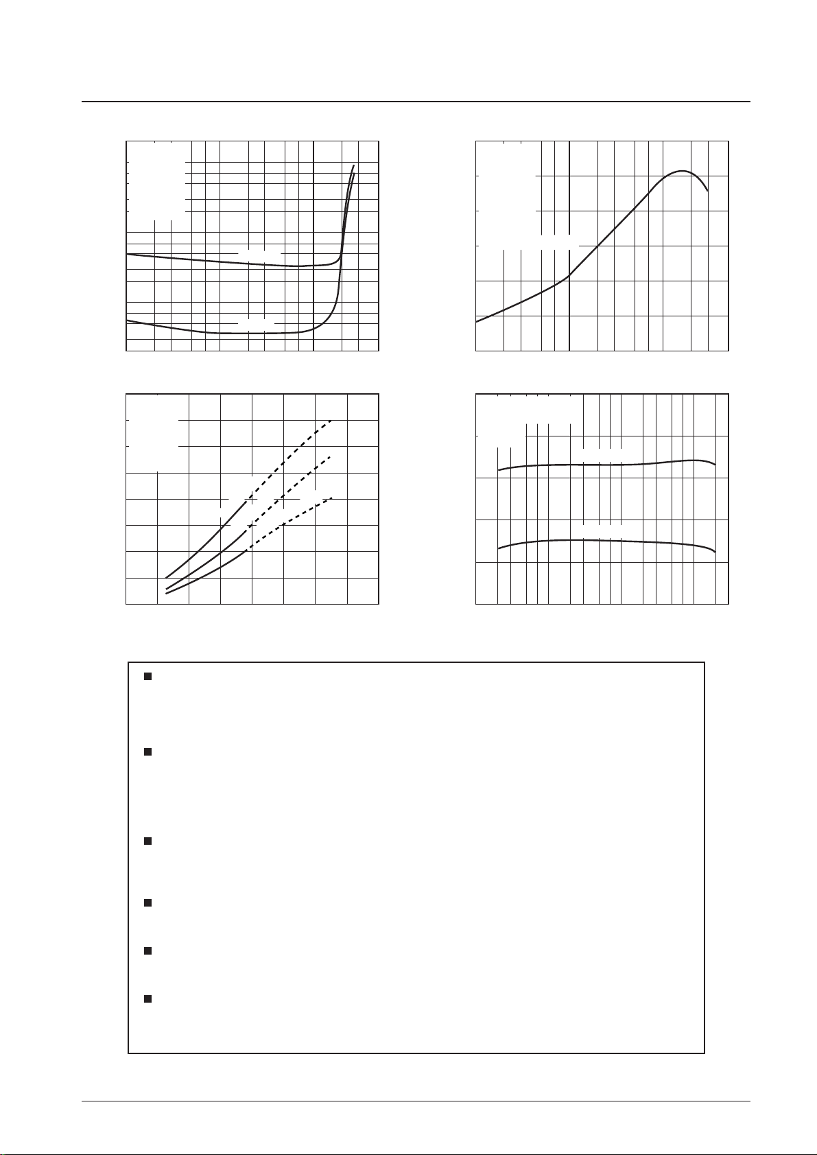
ITF02157
1k10 100
50
40
30
20
10
0
60
100
80
90
70
2 3 5 7 2 3 5 7 2 3 5 7 2 3 5 7
10k 100k
RL = 6 Ω, V
CC
= ±32 V, THD = 10 %
RL = 6 Ω, V
CC
= ±32 V, THD = 0.4 %
Tc = 25 °C
VG = 30 dB
Rg = 600 Ω
P
O
-- f
Output power, P
O
-- W
Frequency, f - Hz
ITF02155
0.001
1.00.1
0.01
7
5
3
2
0.1
7
5
3
2
1.0
7
5
3
2
10
7
5
3
2
100
7
5
3
2
2 3 5 72 3 5 7
10
2 3 5 7
100
20 kHz
20 Hz
1 kHz
Tc = 25 °C
V
CC
= ±32 V
VG = 30 dB
RL = 6 Ω
Rg = 600 Ω
THD -- P
O
Total harmonic distortion, THD
-- %
Output power, P
O
-- W
ITF02168
0
1.00.1
80
60
70
50
40
30
20
10
2 3 5 72 3 5 7
10
2 3 5 7
100
RL = 6 Ω
V
CC
= ±32 V
f = 1kHz
VG = 30 dB
Rg = 600 Ω
2ch drive
Pd -- P
O
Total device power dissipation Pd
-- W
Output power, PO / ch -- W
This catalog provides information as of December, 2002. Specifications and information herein are
subject to change without notice.
Specifications of any and all SANYO products described or contained herein stipulate the performance,
characteristics, and functions of the described products in the independent state, and are not guarantees
of the performance, characteristics, and functions of the described products as mounted in the customer’s
products or equipment. To verify symptoms and states that cannot be evaluated in an independent device,
the customer should always evaluate and test devices mounted in the customer’s products or equipment.
SANYO Electric Co., Ltd. strives to supply high-quality high-reliability products. However, any and all
semiconductor products fail with some probability. It is possible that these probabilistic failures could
give rise to accidents or events that could endanger human lives, that could give rise to smoke or fire,
or that could cause damage to other property. When designing equipment, adopt safety measures so
that these kinds of accidents or events cannot occur. Such measures include but are not limited to protective
circuits and error prevention circuits for safe design, redundant design, and structural design.
In the event that any or all SANYO products (including technical data, services) described or contained
herein are controlled under any of applicable local export control laws and regulations, such products must
not be exported without obtaining the export license from the authorities concerned in accordance with the
above law.
No part of this publication may be reproduced or transmitted in any form or by any means, electronic or
mechanical, including photocopying and recording, or any information storage or retrieval system,
or otherwise, without the prior written permission of SANYO Electric Co., Ltd.
Any and all information described or contained herein are subject to change without notice due to
product/technology improvement, etc. When designing equipment, refer to the “Delivery Specification”
for the SANYO product that you intend to use.
Information (including circuit diagrams and circuit parameters) herein is for example only; it is not
guaranteed for volume production. SANYO believes information herein is accurate and reliable, but
no guarantees are made or implied regarding its use or any infringements of intellectual property rights
or other rights of third parties.
Page 14

Ordering number : ENN7374
D2503TN (OT) No. 7374-1/8
Overview
The STK403-400 series products are audio power
amplifier hybrid ICs that consist of optimally-designed
discrete component power amplifier circuits that have
been miniaturized using SANYO's unique insulated metal
substrate technology (IMST). The adoption of a newlydeveloped low thermal resistance substrate allows this
product to integrate six power amplifier channels in a
single compact package. The adoption of a standby circuit
in this device allows it to reduce impulse noise
significantly as compared to earlier Sanyo products, in
particular, the STK402-*00 series products.
Features
• Series of pin compatible power amplifiers ranging from
30 W/ch to 45 W/ch (10%/1 kHz) devices. The same
printed circuit board can be used depending on the
output power grade.
• Miniature packages
— 78.0 mm × 32.0 mm × 9.0 mm *
*: Not including the pins.
• Output load impedance: RL= 6 Ω
• Allowable load shorted time: 0.3 seconds
• Supports the use of standby and muting circuits.
Package Dimensions
unit: mm
4202-SIP28
SANYO: SIP28
[STK403-430]
STK403-430
SANYO Electric Co.,Ltd. Semiconductor Company
TOKYO OFFICE Tokyo Bldg., 1-10, 1 Chome, Ueno, Taito-ku, TOKYO, 110-8534 JAPAN
Six-Channel Class AB Audio Power Amplifier IC
20 W
× 6 Channels
Thick-Film Hybrid IC
Any and all SANYO products described or contained herein do not have specifications that can handle
applications that require extremely high levels of reliability, such as life-support systems, aircraft’s
control systems, or other applications whose failure can be reasonably expected to result in serious
physical and/or material damage. Consult with your SANYO representative nearest you before using
any SANYO products described or contained herein in such applications.
SANYO assumes no responsibility for equipment failures that result from using products at values that
exceed, even momentarily, rated values (such as maximum ratings, operating condition ranges, or other
parameters) listed in products specifications of any and all SANYO products described or contained
herein.
Page 15
No. 7374-2/8
STK403-430
Item
Type No.
STK403-430 STK403-440 STK403-450
Output 1 (10%/1 kHz) 30 W × 6 ch 40 W × 6 ch 45 W × 6 ch
Output 2 (0.6%/20 Hz to 20 kHz)
20 W × 6 ch 25 W × 6 ch 30 W × 6 ch
Maximum supply voltage (No signal) ±36 V ±38 V ±40 V
Maximum supply voltage (6 Ω) ±34 V ±36 V ±38 V
Recommended supply voltage (6 Ω) ±23 V ±26 V ±28 V
Package 78.0 mm × 32.0 mm × 9.0 mm
Series Organization
Specifications
Maximum Ratings at Ta = 25°C
These products are organized as a series based on their output capacity.
Operating Characteristics at Tc = 25°C, RL= 6 Ω (noninductive load), Rg = 600 Ω, VG = 30 dB
Notes: 1. 1ch drive
2. Unless otherwise noted, use a constant-voltage supply for the power supply used during inspection.
3. Use the transformer power supply circuit shown in the figure below for allowable load shorted time measurement and output noise voltage
measurement.
4. The output noise voltage values shown are peak values read with a VTVM. However, an AC stabilized (50 Hz) power supply should be used to
minimize the influence of AC primary side flicker noise on the reading.
5. Design applications so that the minus pre-V
CC
line (pin 17) is the lowest potential applied to the IC at all times.
6. A limiting resistor that assures that the maximum operating current flowing into the standby pin (pin 23) does not exceed the maximum rating must
be included in application circuits. This IC operates when a voltage higher than V
BE
(about 0.6 V) is applied to the standby pin.
4700µF
4700µF
DBA30C
500Ω
500Ω
+V
CC
--V
CC
+
+
Designated Transformer Power Supply (RP-25 equivalent)
Parameter Symbol Conditions Ratings Unit
Maximum supply voltage (No signal) V
CC
max(0) ±36 V
Maximum supply voltage V
CC
max(1) RL≥ 6 Ω ±34 V
Minimum operating supply voltage V
CC
min ±10 V
Maximum operation flow-in current (pin 23)
I
ST OFF
max 1.2 mA
Thermal resistance θj-c Per power transistor 3.6 °C/W
Junction temperature Tj max
Both the Tj max and the Tc max conditions must be met.
150 °C
Operating IC substrate temperature Tc max 125 °C
Storage temperature Tstg –30 to +125 °C
Allowable load shorted time *
4
ts VCC= ±23.0 V, RL= 6 Ω, f = 50 Hz, PO= 20 W, 1ch drive 0.3 s
Parameter Symbol
Conditions*
1
Ratings
Unit
V
CC
(V) f (Hz) PO(W) THD (%) min typ max
P
O
(1) ±23.0 20 to 20 k 0.6 18 20
Output power *
1
PO(2) ±23.0 1 k 10 30
W
THD (1) ±23.0 20 to 20 k 5.0 VG = 30 dB 0.6
Total harmonic distortion *
1
THD (2) ±23.0 1 k 5.0 VG = 30 dB 0.03
%
Frequency characteristics f
L
, f
H
±23.0 1.0 +0 –3 dB
20 to 50 k
Hz
Input impedance ri ±23.0 1 k 1.0 55 kΩ
Output noise voltage *
2
V
NO
±28.0 Rg = 2.2 kΩ 1.0 mVrms
Quiescent current I
CCO
±28.0 No loading 60 110 180 mA
Neutral voltage V
N
±28.0 –70 0 +70 mV
Current flowing into pin 23
I
ST ON
±23.0
V23= 5 V, current Limiting
0 mA
in standby mode *
6
resistance: 6.2 kΩ
Current flowing into pin 23
I
ST OFF
±23.0 0.4 1.2 mA
in operating mode *
6
Page 16
No. 7374-3/8
STK403-430
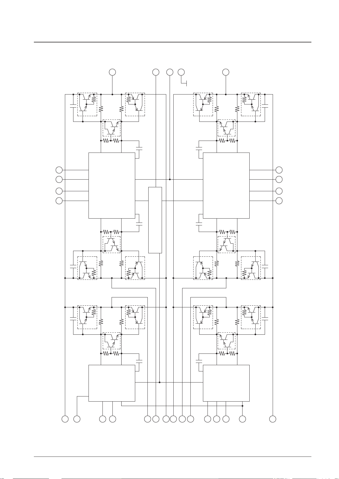
Internal Equivalent Circuit
11
5 6 7 8
9
23
19
18
2
3
4
1
10
12
13
16
15
Pre Driver IC
(CH2 / CH3)
Pre Driver IC
(CH1)
Bias Circuit
24 25 26 27
28
Pre Driver IC
(CH5 / CH6)
22
21
20
17
14
Pre Driver IC
(CH4)
ITF02247
C13
TR7
TR8
TR17
SUB
TR16
C16
C12
TR4
TR5
C15
TR13
TR14
C11
TR1
TR2
C14
TR10
TR11
TR9
R24
R25
TR6
R22
R23
TR3
R20
R21
R5
R6
R3
R4
R1
R2
TR12
R27
R26
TR15
R29
R28
TR18
R31
R30
R8
R7
R10
R9
R12
R11
C3C2
C1
C4
C5 C6
Page 17
No. 7374-4/8
STK403-430
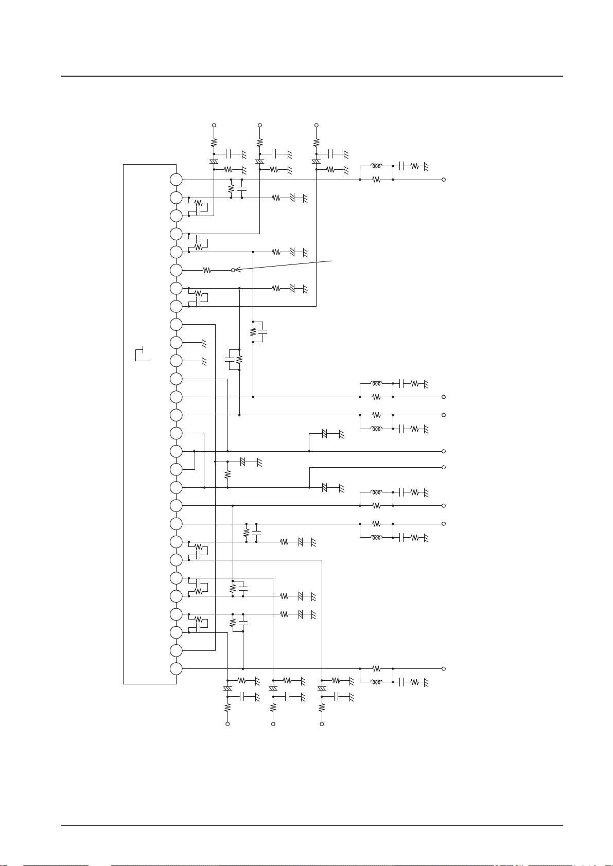
Sample Application Circuit
28272625242322212019181716151413121110
987654321
STK403-400 series
Ch1
OUT
+PRE --PRE
Ch1
IN
Ch1
NF
Ch2
NF
Ch2
IN
Ch3
IN
Ch3
NF
Ch3
OUT
Ch2
OUT
+V
CC
- -V
CC
- -V
CC
+V
CC
Ch4
OUT
Ch5
OUT
SUB
GND
GND
SUB
+PRE
Ch4
IN
Ch4
NF
BIAS
(ST-BY)
Ch5
NF
Ch5
IN
Ch6
IN
Ch6
NF
Ch6
OUT
Ch6
IN
Ch1
IN
Ch2
IN
Ch3
IN
Ch5
IN
Ch4
IN
1kΩ2.2µF
3µF
0.1µF
10µF
100µF
1kΩ2.2µF
1kΩ2.2µF
56kΩ
470pF
1kΩ 2.2µF
56kΩ
470pF
1kΩ 2.2µF
56kΩ
470pF
1kΩ 2.2µF
56kΩ
470pF
56kΩ
1.8kΩ
3kΩ
3kΩ
3kΩ
6.2kΩ
10µF 1.8kΩ
10µF
470µF
470µF
1.8kΩ
10µF 1.8kΩ
10µF 1.8kΩ
10µF 1.8kΩ
56kΩ
56kΩ56kΩ
100Ω
470pF
4.7Ω
4.7Ω
3µF
0.1µF
4.7Ω
4.7Ω
4.7Ω
3µF
0.1µF
4.7Ω
3µF
0.1µF
4.7Ω
4.7Ω
4.7Ω
3µF
0.1µF
4.7Ω
4.7Ω
3µF
0.1µF
4.7Ω
3pF
3pF
56kΩ
3pF
56kΩ
3pF
56kΩ
3pF
3pF
56kΩ
470pF
220pF
220pF
220pF
3kΩ
3kΩ
3kΩ
220pF
220pF
220pF
+
+
+
+++
+
+
+
+++
+
+
+
Stand-by
Control
(*1)
Ch6
OUT
Ch5
OUT
Ch4
OUT
--V
CC
+V
CC
Ch2
OUT
Ch3
OUT
Ch1
OUT
ITF02248
*1. Use a value for the limiting resistor that assures that the maximum operating current flowing into the standby pin (pin 23) does not exceed the maximum rating.
Page 18

No. 7374-5/8
STK403-430
Thermal Design Example
The heat sink thermal resistance, θc-a, required to handle the total power dissipated within this hybrid IC is determined as
follows.
Condition 1: The IC substrate temperature Tc must not exceed 125°C.
Pd × θc – a + Ta < 125°C ... (1)
Ta: Guaranteed ambient temperature for the end product.
Condition 2: The junction temperature of each individual transistor must not exceed 150°C.
Pd × θc – a + Pd/N × θj – c + Ta < 150°C ... (2)
N: Number of power transistors
θj-c: Thermal resistance per power transistor
We take the power dissipation in the power transistors to be Pd evenly distributed across those N power transistors.
If we solve for θc-a in equations (1) and (2), we get the following inequalities.
θc – a < (125 – Ta)/Pd ... (1)’
θc – a < (150 – Ta)/Pd – θj-c/N ... (2)’
Values that satisfy both these inequalities at the same time are the required heat sink thermal resistance values.
Determining the following specifications allows us to determine the required heat sink thermal resistance from
inequalities (1)’ and (2)’.
• Supply voltage: V
CC
• Load resistance: R
L
• Guaranteed ambient temperature: Ta
Example:
Assume that the IC supply voltage, VCC, is ±23 V, RLis 6 Ω, and that the signal is a continuous sine wave. In this case,
from the Pd – POcharacteristics, the maximum power will be 103 W for a signal with a frequency of 1 kHz.
For actual music signals, it is usual to use a Pd of 1/8 of POmax, which is the power estimated for continuous signals in
this manner. (Note that depending on the particular safety standard used, a value somewhat different from the value of
1/8 used here may be used.)
That is:
Pd = 65 W (when 1/8 POmax is 2.5 W)
The number, N, of power transistors in the hybrid IC's audio amplifier block is 12. Since the thermal resistance, θc-a, per
transistor is 3.6°C/W, the required heat sink thermal resistance, θc-a, for a guaranteed ambient temperature of 50°C will
be as follows.
From inequality (1)’: θc – a < (125 – 50)/65
< 1.15
From inequality (2)’: θc – a < (150 – 50)/65 – 3.6/12
< 1.23
Therefore, the thermal resistance that satisfies both these expressions at the same time is 1.15°C/W.
Note that this thermal design example assumes the use of a constant-voltage power supply, and is only provided as an
example for reference purposes. Thermal designs must be tested in an actual end product.
Page 19

No. 7374-6/8
STK403-430
Stand-by & Mute Sample Application Circuit
28272625242322212019181716151413121110
987654321
STK403-400 series
Ch1
OUT
+PRE --PRE
Ch1
IN
Ch1
NF
Ch2
NF
Ch2
IN
Ch3
IN
Ch3
NF
Ch3
OUT
Ch2
OUT
+V
CC
- -V
CC
- -V
CC
+V
CC
Ch4
OUT
Ch5
OUT
SUB
GND
GND
SUB
+PRE
Ch4
IN
Ch4
NF
BIAS
(ST-BY)
Ch5
NF
Ch5
IN
Ch6
IN
Ch6
NF
Ch6
OUT
Ch6
IN
Ch1
IN
Ch2
IN
Ch3
IN
Ch5
IN
Ch4
IN
10kΩ
10kΩ
10kΩ
2.2kΩ
10kΩ
+
+
+
+++
+
+
+
+
+++
+
+
+
Ch6
OUT
Ch5
OUT
Ch4
OUT
--V
CC
+V
CC
Ch2
OUT
Ch3
OUT
Ch1
OUT
ITF02249
*1. Use a value for the limiting resistor that assures that the maximum operating current
flowing into the standby pin (pin 23) does not exceed the maximum rating.
10kΩ
10kΩ
10kΩ
2.2kΩ
10kΩ
3kΩ
33kΩ
2kΩ
33µF
6.2kΩ
Mute Control
H : Single Mute
L : Normal
Mute Control
H : Single Mute
L : Normal
(*1)
Stand-by
Control
H : Operation
L : Stand-by
Stand-by
Control
Mute
Control
+5
+5
ST-BY ST-BYPLAY
MUTE
MUTE
Page 20
No. 7374-7/8
STK403-430
Standby Mode Control
28272625242322212019181716151413121110
987654321
STK403-400 series
Ch1
OUT
+PRE --PRE
Ch1
IN
Ch1
NF
Ch2
NF
Ch2
IN
Ch3
IN
Ch3
NF
Ch3
OUT
Ch2
OUT
+V
CC
- -V
CC
- -V
CC
+V
CC
Ch4
OUT
Ch5
OUT
SUB
GND
GND
SUB
+PRE
Ch4
IN
Ch4
NF
BIAS
(ST-BY)
Ch5
NF
Ch5
IN
Ch6
IN
Ch6
NF
Ch6
OUT
+
ITF02250
3kΩ
33kΩ
2kΩ
33µF
/ 10V
6.2kΩ
(*1)
Stand-by Control
H : Operation Mode (+5 V)
L : Stand-by Mode (0 V)
R1
I
ST
=(applied voltage–V
BE
×2) / R1
=(5--0.6×2) / 6.2kΩ
≈0.63(mA)
Current flowing in I
ST
ITF02263
V : 200mV / 1div
T : 100ms / 1div
OFF
(Stand-by
Mode)
ON
(Operation
Mode)
0.1V
0.16V
• Applied voltage V
ST
... An internal transistor turns on when a voltage over 0.6 V is applied
and the IC transitions to operating mode.
• Current flowing into pin 23 IST ... Use a value for the limiting resistor that assures that the maximum
operating current flowing into this pin due to the control voltage applied
by the microcontroller or other circuit does not exceed the maximum rating.
• Impulse noise that occurs at power on and power off can be reduced significantly by using a standby circuit.
• End product design is made easier by using a limiting resistor *1 to match the control voltage provided by the microcontroller or other control circuit.
• Standby control can be applied by controlling the current (I
ST
) flowing into the standby pin (pin 23).
Page 21
PS No. 7374-8/8
STK403-430
This catalog provides information as of December, 2003. Specifications and information herein are
subject to change without notice.
Specifications of any and all SANYO products described or contained herein stipulate the performance,
characteristics, and functions of the described products in the independent state, and are not guarantees
of the performance, characteristics, and functions of the described products as mounted in the customer’s
products or equipment. To verify symptoms and states that cannot be evaluated in an independent device,
the customer should always evaluate and test devices mounted in the customer’s products or equipment.
SANYO Electric Co., Ltd. strives to supply high-quality high-reliability products. However, any and all
semiconductor products fail with some probability. It is possible that these probabilistic failures could
give rise to accidents or events that could endanger human lives, that could give rise to smoke or fire,
or that could cause damage to other property. When designing equipment, adopt safety measures so
that these kinds of accidents or events cannot occur. Such measures include but are not limited to protective
circuits and error prevention circuits for safe design, redundant design, and structural design.
In the event that any or all SANYO products (including technical data, services) described or contained
herein are controlled under any of applicable local export control laws and regulations, such products must
not be exported without obtaining the export license from the authorities concerned in accordance with the
above law.
No part of this publication may be reproduced or transmitted in any form or by any means, electronic or
mechanical, including photocopying and recording, or any information storage or retrieval system,
or otherwise, without the prior written permission of SANYO Electric Co., Ltd.
Any and all information described or contained herein are subject to change without notice due to
product/technology improvement, etc. When designing equipment, refer to the “Delivery Specification”
for the SANYO product that you intend to use.
Information (including circuit diagrams and circuit parameters) herein is for example only; it is not
guaranteed for volume production. SANYO believes information herein is accurate and reliable, but
no guarantees are made or implied regarding its use or any infringements of intellectual property rights
or other rights of third parties.
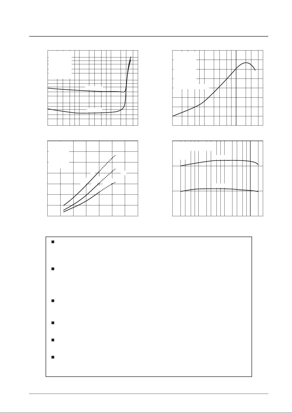
Total harmonic distortion, THD — %
— W
Output power, P
2
10
7
5
3
2
1.0
7
5
3
2
0.1
7
5
3
2
80
70
60
50
O
40
30
20
10
VCC=±23V
RL=6Ω
VG=30dB
Rg=600Ω
Tc=25°C
6ch Drive
RL=6Ω
f=1kHz
VG=30dB
Rg=600Ω
Tc=25°C
6ch Drive
THD — P
O
f=20kHz
f=1kHz
2 3 5 2 3 572 3 5 7
1.00.1
Output power, PO — W
PO — V
CC
THD=10%
THD=0.6%
f=20kHz, THD=0.6%
120
100
VCC=
RL=6
f=1kHz
Pd — P
±23V
Ω
O
VG=30dB
Rg=600Ω
80
Tc=25°C
6ch Drive
(same output rating)
60
40
20
Total device power dissipation, Pd — WOutput power, P
0
10
ITF02251
2 3 5 7 2 3 5 2 3 57
1.00.1
Output power, P
40
VCC=±23V, RL=6Ω
O
PO — f
— W
10
ITF02252
VG=30dB, Rg=600Ω
Tc=25°C
35
6ch drive
THD=10%
— W
O
30
25
THD=0.6%
20
0
10 14 18 22 26 30 34 38 42
Supply voltage, ±V
CC
— V
ITF02253
15
2 3 5 7 2 3 5 7 2 3 5 7 2 3
Frequency, f — Hz
1k10 100
10k
ITF02254
Page 22
Ordering number : ENN*7375
21604TN (OT) No. 7375-1/8
Overview
The STK403-400 series products are audio power
amplifier hybrid ICs that consist of optimally-designed
discrete component power amplifier circuits that have
been miniaturized using SANYO’s unique insulated metal
substrate technology (IMST). The adoption of a newlydeveloped low thermal resistance substrate allows this
product to integrate six power amplifier channels in a
single compact package. The adoption of a standby circuit
in this device allows it to reduce impulse noise
significantly as compared to earlier Sanyo products, in
particular, the STK402-*00 series products.
Features
• Series of pin compatible power amplifiers ranging from
30 W/ch to 45 W/ch (10%/1 kHz) devices. The same
printed circuit board can be used depending on the
output power grade.
• Miniature packages
— 78.0 mm × 32.0 mm × 9.0 mm *
*: Not including the pins.
• Output load impedance: RL= 6 Ω
• Allowable load shorted time: 0.3 seconds
• Supports the use of standby and muting circuits.
Package Dimensions
unit: mm
4202-SIP28
Preliminary
SANYO: SIP28
[STK403-440]
STK403-440
SANYO Electric Co.,Ltd. Semiconductor Company
TOKYO OFFICE Tokyo Bldg., 1-10, 1 Chome, Ueno, Taito-ku, TOKYO, 110-8534 JAPAN
Six-Channel Class AB Audio Power Amplifier IC
25 W × 6 Channels
Thick-Film Hybrid IC
Any and all SANYO products described or contained herein do not have specifications that can handle
applications that require extremely high levels of reliability, such as life-support systems, aircraft’s
control systems, or other applications whose failure can be reasonably expected to result in serious
physical and/or material damage. Consult with your SANYO representative nearest you before using
any SANYO products described or contained herein in such applications.
SANYO assumes no responsibility for equipment failures that result from using products at values that
exceed, even momentarily, rated values (such as maximum ratings, operating condition ranges, or other
parameters) listed in products specifications of any and all SANYO products described or contained
herein.
Page 23

No. 7375-2/8
STK403-440
Item
Type No.
STK403-430 STK403-440 STK403-450
Output 1 (10%/1 kHz) 30 W × 6 ch 40 W × 6 ch 45 W × 6 ch
Output 2 (0.6%/20 Hz to 20 kHz)
20 W × 6 ch 25 W × 6 ch 30 W × 6 ch
Maximum supply voltage (No signal) ±36 V ±38 V ±40 V
Maximum supply voltage (6 Ω) ±34 V ±36 V ±38 V
Recommended supply voltage (6 Ω) ±23 V ±26 V ±28 V
Package 78.0 mm × 32.0 mm × 9.0 mm
Series Organization
Specifications
Maximum Ratings at Ta = 25°C
These products are organized as a series based on their output capacity.
Operating Characteristics at Tc = 25°C, RL= 6 Ω (noninductive load), Rg = 600 Ω, VG = 30 dB
Notes: 1. 1ch drive
2. Unless otherwise noted, use a constant-voltage supply for the power supply used during inspection.
3. The output noise voltage values shown are peak values read with a VTVM. However, an AC stabilized (50 Hz) power supply should be used to
minimize the influence of AC primary side flicker noise on the reading.
4. Use the transformer power supply circuit shown in the figure below for allowable load shorted time measurement and output noise voltage
measurement.
5. Design applications so that the minus pre-V
CC
line (pin 17) is at the lowest potential at all times.
6. A limiting resistor that assures that the maximum operating current flowing into the standby pin (pin 23) does not exceed the maximum rating must
be included in application circuits. This IC operates when a voltage higher than V
BE
(about 0.6 V) is applied to the standby pin.
4700 µF
4700 µF
DBA30C
500 Ω
500 Ω
+V
CC
--V
CC
+
+
Designated Transformer Power Supply (RP-25 equivalent)
Parameter Symbol Conditions Ratings Unit
Maximum supply voltage (No signal) V
CC
max(0) ±38 V
Maximum supply voltage V
CC
max(1) RL≥ 6 Ω ±36 V
Minimum operating supply voltage V
CC
min ±10 V
Maximum operation flow-in current (pin 23)
I
ST OFF
max 1.2 mA
Thermal resistance θj-c Per power transistor 3.6 °C/W
Junction temperature Tj max
Both the Tj max and the Tc max conditions must be met.
150 °C
Operating IC substrate temperature Tc max 125 °C
Storage temperature Tstg –30 to +125 °C
Allowable load shorted time *
4
ts VCC= ±26.0 V, RL= 6 Ω, f = 50 Hz, PO= 25 W, 1ch drive 0.3 s
Parameter Symbol
Conditions*
1
Ratings
Unit
V
CC
(V) f (Hz) PO(W) THD (%) min typ max
P
O
(1) ±26.0 20 to 20 k 0.6 23 25
Output power *
1
PO(2) ±26.0 1 k 10 40
W
THD (1) ±26.0 20 to 20 k 5.0 VG = 30 dB 0.6
Total harmonic distortion *
1
THD (2) ±26.0 1 k 5.0 VG = 30 dB 0.03
%
Frequency characteristics f
L
, f
H
±26.0 1.0 +0 –3 dB
20 to 50 k
Hz
Input impedance ri ±26.0 1 k 1.0 55 kΩ
Output noise voltage *
2
V
NO
±31.0 Rg = 2.2 kΩ 1.0 mVrms
Quiescent current I
CCO
±31.0 No loading 60 110 180 mA
Neutral voltage V
N
±31.0 –70 0 +70 mV
Current flowing into pin 23
I
ST ON
±26.0
V23= 5 V, current limiting
0 mA
in standby mode *
6
resistance: 6.2 kΩ
Current flowing into pin 23
I
ST OFF
±26.0 0.4 1.2 mA
in operating mode *
6
Page 24
No. 7375-3/8
STK403-440
Internal Equivalent Circuit
11
5 6 7 8
9
23
19
18
2
3
4
1
10
12
13
16
15
Pre driver IC
(CH2 / CH3)
Pre driver IC
(CH1)
Bias circuit
24 25 26 27
28
Pre driver IC
(CH5 / CH6)
22
21
20
17
14
Pre driver IC
(CH4)
ITF02247
C13
TR7
TR8
TR17
SUB
TR16
C16
C12
TR4
TR5
C15
TR13
TR14
C11
TR1
TR2
C14
TR10
TR11
TR9
R24
R25
TR6
R22
R23
TR3
R20
R21
R5
R6
R3
R4
R1
R2
TR12
R27
R26
TR15
R29
R28
TR18
R31
R30
R8
R7
R10
R9
R12
R11
C3C2
C1
C4
C5 C6
Page 25
No. 7375-4/8
STK403-440
Sample Application Circuit
28272625242322212019181716151413121110
987654321
STK403-400 series
Ch1
OUT
+PRE --PRE
Ch1
IN
Ch1
NF
Ch2
NF
Ch2
IN
Ch3
IN
Ch3
NF
Ch3
OUT
Ch2
OUT
+V
CC
- -V
CC
- -V
CC
+V
CC
Ch4
OUT
Ch5
OUT
SUB
GND
GND
SUB
+PRE
Ch4
IN
Ch4
NF
BIAS
(ST-BY)
Ch5
NF
Ch5
IN
Ch6
IN
Ch6
NF
Ch6
OUT
Ch6
IN
Ch1
IN
Ch2
IN
Ch3
IN
Ch5
IN
Ch4
IN
1 kΩ2.2 µF
3 µF
0.1 µF
10 µF
100 µF
1 kΩ2.2 µF
1 kΩ2.2 µF
56 kΩ
470 pF
1 kΩ 2.2 µF
56 kΩ
470 pF
1 kΩ 2.2 µF
56 kΩ
470 pF
1 kΩ 2.2 µF
56 kΩ
470 pF
56 kΩ
1.8 kΩ
3 kΩ
3 kΩ
3 kΩ
6.2 kΩ
10 µF 1.8 kΩ
10 µF
470 µF
470 µF
1.8 kΩ
10 µF 1.8 kΩ
10 µF 1.8 kΩ
10 µF 1.8 kΩ
56 kΩ
56 kΩ56 kΩ
100 Ω
470 pF
4.7 Ω
4.7 Ω
3 µF
0.1 µF
4.7 Ω
4.7 Ω
4.7 Ω
3 µF
0.1 µF
4.7 Ω
3 µF
0.1 µF
4.7 Ω
4.7 Ω
4.7 Ω
3 µF
0.1 µF
4.7 Ω
4.7 Ω
3 µF
0.1 µF
4.7 Ω
3 pF
3 pF
56 kΩ
3 pF
56 kΩ
3 pF
56 kΩ
3 pF
3 pF
56 kΩ
470 pF
220 pF
220 pF
220 pF
3 kΩ
3 kΩ
3 kΩ
220 pF
220 pF
220 pF
+
+
+
+++
+
+
+
+++
+
+
+
Stand-by
control
*
Ch6
OUT
Ch5
OUT
Ch4
OUT
--V
CC
+V
CC
Ch2
OUT
Ch3
OUT
Ch1
OUT
ITF02248
*: Use a value for the limiting resistor that assures that the maximum operating current flowing into the standby pin (pin 23) does not exceed the maximum rating.
Page 26

No. 7375-5/8
STK403-440
Thermal Design Example
The heat sink thermal resistance, θc-a, required to handle the total power dissipated within this hybrid IC is determined as
follows.
Condition 1: The IC substrate temperature Tc must not exceed 125°C.
Pd × θc-a + Ta < 125°C ... (1)
Ta: Guaranteed ambient temperature for the end product.
Condition 2: The junction temperature of each transistor must not exceed 150°C.
Pd × θc-a + Pd/N × θj-c + Ta < 150°C ... (2)
N: Number of power transistors
θj-c: Thermal resistance per power transistor
We take the power dissipation in the power transistors to be Pd evenly distributed across those N power transistors.
If we solve for θc-a in equations (1) and (2), we get the following inequalities.
θc-a < (125 – Ta)/Pd ... (1)’
θc-a < (150 – Ta)/Pd – θj-c/N ... (2)’
Values that satisfy both these inequalities at the same time are the required heat sink thermal resistance values.
Determining the following specifications allows us to obtain the required heat sink thermal resistance from inequalities
(1)’ and (2)’.
• Supply voltage: V
CC
• Load resistance: R
L
• Guaranteed ambient temperature: Ta
Example:
Assume that the IC supply voltage, VCC, is ±26 V, RLis 6 Ω, and that the signal is a continuous sine wave. In this case,
from the Pd – POcharacteristics, the maximum power will be 134 W for a signal with a frequency of 1 kHz.
For actual music signals, it is usual to use a Pd of 1/8 of POmax, which is the power estimated for continuous signals in
this manner. (Note that depending on the particular safety standard used, a value somewhat different from the value of
1/8 used here may be used.)
That is:
Pd = 85 W (when 1/8 POmax is 3.1 W)
The number, N, of power transistors in the hybrid IC's audio amplifier block is 12. Since the thermal resistance, θj-c, per
transistor is 3.6°C/W, the required heat sink thermal resistance, θc-a, for a guaranteed ambient temperature of 50°C will
be as follows.
From inequality (1)’: θc-a < (125 – 50)/85
< 0.88
From inequality (2)’: θc-a < (150 – 50)/85 – 3.6/12
< 0.87
Therefore, the thermal resistance that satisfies both these expressions at the same time is 0.87°C/W.
Note that this thermal design example assumes the use of a constant-voltage power supply, and is only provided as an
example for reference purposes. Thermal designs must be tested in an actual end product.
Page 27
No. 7375-6/8
STK403-440
Stand-by & Mute Sample Application Circuit
28272625242322212019181716151413121110
987654321
STK403-400 series
Ch1
OUT
+PRE --PRE
Ch1
IN
Ch1
NF
Ch2
NF
Ch2
IN
Ch3
IN
Ch3
NF
Ch3
OUT
Ch2
OUT
+V
CC
- -V
CC
- -V
CC
+V
CC
Ch4
OUT
Ch5
OUT
SUB
GND
GND
SUB
+PRE
Ch4
IN
Ch4
NF
BIAS
(ST-BY)
Ch5
NF
Ch5
IN
Ch6
IN
Ch6
NF
Ch6
OUT
Ch6
IN
Ch1
IN
Ch2
IN
Ch3
IN
Ch5
IN
Ch4
IN
10 kΩ
10 kΩ
10 kΩ
2.2 kΩ
10 kΩ
+
+
+
+++
+
+
+
+
+++
+
+
+
Ch6
OUT
Ch5
OUT
Ch4
OUT
--V
CC
+V
CC
Ch2
OUT
Ch3
OUT
Ch1
OUT
ITF02249
*: Use a value for the limiting resistor that assures that the maximum operating current
flowing into the standby pin (pin 23) does not exceed the maximum rating.
10 kΩ
10 kΩ
10 kΩ
2.2 kΩ
10 kΩ
3 kΩ
33 kΩ
2 kΩ
33 µF
6.2 kΩ
Mute control
H : Single mute
L : Normal
Mute control
H : Single mute
L : Normal
*
Stand-by
control
H : Operation
L : Stand-by
Stand-by
control
Mute
control
+5
+5
ST-BY ST-BYPlay
Mute
Mute
Page 28
No. 7375-7/8
STK403-440
Standby Mode Control
28272625242322212019181716151413121110
987654321
STK403-400 series
Ch1
OUT
+PRE --PRE
Ch1
IN
Ch1
NF
Ch2
NF
Ch2
IN
Ch3
IN
Ch3
NF
Ch3
OUT
Ch2
OUT
+V
CC
- -V
CC
- -V
CC
+V
CC
Ch4
OUT
Ch5
OUT
SUB
GND
GND
SUB
+PRE
Ch4
IN
Ch4
NF
BIAS
(ST-BY)
Ch5
NF
Ch5
IN
Ch6
IN
Ch6
NF
Ch6
OUT
+
ITF02250
3 kΩ
33 kΩ
2 kΩ
33 µF
/ 10 V
6.2 kΩ *
Stand-by control
H : Operation mode (+5 V)
L : Stand-by mode (0 V)
R1
I
ST
= (applied voltage – V
BE
× 2) / R1
= (5--0.6 × 2) / 6.2 kΩ
≈ 0.63 (mA)
Current flowing in I
ST
ITF02263
V : 200 mV / 1div
T : 100 ms / 1div
OFF
(Stand-by
mode)
ON
(Operation
mode)
0.1 V
0.16 V
• Applied voltage (V
ST
) ..................
• Current flowing into pin 23 (I
ST
) ...
An internal transistor turns on when a voltage over 0.6 V is applied
and the IC enters into operating mode.
Use a value for the limiting resistor that assures that the maximum
operating current flowing into this pin due to the control voltage applied
by the microcontroller or other circuit does not exceed the maximum rating.
• Impulse noise that occurs at power on and power off can be reduced significantly by using a standby circuit.
• End product design is made easier by using a limiting resistor (*) to match the control voltage provided by the microcontroller or other control circuit.
• Standby control is available by controlling the current (I
ST
) flowing into the standby pin (pin 23).
Page 29
PS No. 7375-8/8
STK403-440
This catalog provides information as of February, 2004. Specifications and information herein are subject
to change without notice.
Specifications of any and all SANYO products described or contained herein stipulate the performance,
characteristics, and functions of the described products in the independent state, and are not guarantees
of the performance, characteristics, and functions of the described products as mounted in the customer’s
products or equipment. To verify symptoms and states that cannot be evaluated in an independent device,
the customer should always evaluate and test devices mounted in the customer’s products or equipment.
SANYO Electric Co., Ltd. strives to supply high-quality high-reliability products. However, any and all
semiconductor products fail with some probability. It is possible that these probabilistic failures could
give rise to accidents or events that could endanger human lives, that could give rise to smoke or fire,
or that could cause damage to other property. When designing equipment, adopt safety measures so
that these kinds of accidents or events cannot occur. Such measures include but are not limited to protective
circuits and error prevention circuits for safe design, redundant design, and structural design.
In the event that any or all SANYO products (including technical data, services) described or contained
herein are controlled under any of applicable local export control laws and regulations, such products must
not be exported without obtaining the export license from the authorities concerned in accordance with the
above law.
No part of this publication may be reproduced or transmitted in any form or by any means, electronic or
mechanical, including photocopying and recording, or any information storage or retrieval system,
or otherwise, without the prior written permission of SANYO Electric Co., Ltd.
Any and all information described or contained herein are subject to change without notice due to
product/technology improvement, etc. When designing equipment, refer to the “Delivery Specification”
for the SANYO product that you intend to use.
Information (including circuit diagrams and circuit parameters) herein is for example only; it is not
guaranteed for volume production. SANYO believes information herein is accurate and reliable, but
no guarantees are made or implied regarding its use or any infringements of intellectual property rights
or other rights of third parties.
Total harmonic distortion, THD — %
0.01
— W
O
Output power, P
2
V
10
RL = 6 Ω
7
VG = 30 dB
5
Rg = 600 Ω
3
Tc = 25°C
2
6ch drive
1.0
7
5
3
2
0.1
7
5
3
2
70
60
50
40
30
20
= ±26 V
CC
RL = 6 Ω
f = 1 kHz
VG = 30 dB
Rg = 600 Ω
Tc = 25°C
6ch drive
THD — P
O
f = 20 kHz
f = 1 kHz
2 3 5 2 3 57 72 3 5 7
1.00.1
Output power, PO — W
PO — V
THD = 10%
CC
THD = 0.6%
f = 20 kHz, THD = 0.6%
160
140
120
100
80
60
40
20
Total device power dissipation, Pd — W
10
ITF02255
0
50
±26 V
V
=
CC
RL = 6
Ω
f = 1 kHz
VG = 30 dB
Rg = 600 Ω
Tc = 25°C
6ch drive
(same output rating)
2 3 5 7 2 3 5 2 3 57 7
V
= ±26 V, RL = 6 Ω
CC
VG = 30 dB, Rg = 600 Ω
Pd — P
1.00.1
Output power, PO — W
O
10
ITF02256
PO — f
Tc = 25°C
6ch drive
40
— W
O
THD = 10%
THD = 0.6%
30
Output power, P
10
0
10 14 18 22 26 30 34 38
Supply voltage, ±VCC — V
ITF02257
20
2 3 5 7 2 3 5 7 2 3 5 7 2 3
Frequency, f — Hz
1k10 100
10k
ITF02258
Page 30

Ordering number : ENN*7376
21604TN (OT) No. 7376-1/8
Overview
The STK403-400 series products are audio power
amplifier hybrid ICs that consist of optimally-designed
discrete component power amplifier circuits that have
been miniaturized using SANYO’s unique insulated metal
substrate technology (IMST). The adoption of a newlydeveloped low thermal resistance substrate allows this
product to integrate six power amplifier channels in a
single compact package. The adoption of a standby circuit
in this device allows it to reduce impulse noise
significantly as compared to earlier Sanyo products, in
particular, the STK402-*00 series products.
Features
• Series of pin compatible power amplifiers ranging from
30 W/ch to 45 W/ch (10%/1 kHz) devices. The same
printed circuit board can be used depending on the
output power grade.
• Miniature packages
— 78.0 mm × 32.0 mm × 9.0 mm *
*: Not including the pins.
• Output load impedance: RL= 6 Ω
• Allowable load shorted time: 0.3 seconds
• Supports the use of standby and muting circuits.
Package Dimensions
unit: mm
4202-SIP28
Preliminary
SANYO: SIP28
[STK403-450]
STK403-450
SANYO Electric Co.,Ltd. Semiconductor Company
TOKYO OFFICE Tokyo Bldg., 1-10, 1 Chome, Ueno, Taito-ku, TOKYO, 110-8534 JAPAN
Six-Channel Class AB Audio Power Amplifier IC
30 W
×6 Channels
Thick-Film Hybrid IC
Any and all SANYO products described or contained herein do not have specifications that can handle
applications that require extremely high levels of reliability, such as life-support systems, aircraft’s
control systems, or other applications whose failure can be reasonably expected to result in serious
physical and/or material damage. Consult with your SANYO representative nearest you before using
any SANYO products described or contained herein in such applications.
SANYO assumes no responsibility for equipment failures that result from using products at values that
exceed, even momentarily, rated values (such as maximum ratings, operating condition ranges, or other
parameters) listed in products specifications of any and all SANYO products described or contained
herein.
Page 31

No. 7376-2/8
STK403-450
Item
Type No.
STK403-430 STK403-440 STK403-450
Output 1 (10%/1 kHz) 30 W
×6 ch 40 W ×6 ch 45 W ×6 ch
Output 2 (0.6%/20 Hz to 20 kHz)
20 W ×6 ch 25 W ×6 ch 30 W ×6 ch
Maximum supply voltage (No signal) ±36 V ±38 V ±40 V
Maximum supply voltage (6 Ω) ±34 V ±36 V ±38 V
Recommended supply voltage (6 Ω) ±23 V ±26 V ±28 V
Package 78.0 mm × 32.0 mm × 9.0 mm
Series Organization
Specifications
Maximum Ratings at Ta = 25°C
These products are organized as a series based on their output capacity.
Operating Characteristics at Tc = 25°C, RL= 6 Ω (noninductive load), Rg = 600 Ω, VG = 30 dB
Notes: 1. 1ch drive
2. Unless otherwise noted, use a constant-voltage supply for the power supply used during inspection.
3. The output noise voltage values shown are peak values read with a VTVM. However, an AC stabilized (50 Hz) power supply should be used to
minimize the influence of AC primary side flicker noise on the reading.
4. Use the transformer power supply circuit shown in the figure below for allowable load shorted time measurement and output noise voltage
measurement.
5. Design applications so that the minus pre-V
CC
line (pin 17) is at the lowest potential at all times.
6. A limiting resistor that assures that the maximum operating current flowing into the standby pin (pin 23) does not exceed the maximum rating must
be included in application circuits. This IC operates when a voltage higher than V
BE
(about 0.6 V) is applied to the standby pin.
4700 µF
4700 µF
DBA30C
500 Ω
500 Ω
+V
CC
--V
CC
+
+
Designated Transformer Power Supply (RP-25 equivalent)
Parameter Symbol Conditions Ratings Unit
Maximum supply voltage (No signal) V
CC
max(0) ±40 V
Maximum supply voltage V
CC
max(1) RL= 6 Ω ±38 V
Minimum operating supply voltage V
CC
min ±10 V
Maximum operation flow-in current (pin 23)
I
ST OFF
max 1.2 mA
Thermal resistance θj-c Per power transistor 3.6 °C/W
Junction temperature Tj max
Both the Tj max and the Tc max conditions must be met.
150 °C
Operating IC substrate temperature Tc max 125 °C
Storage temperature Tstg –30 to +125 °C
Allowable load shorted time *
4
ts VCC= ±28.0 V, RL= 6 Ω, f = 50 Hz, PO= 30 W, 1ch drive 0.3 s
Parameter Symbol
Conditions*
1
Ratings
Unit
V
CC
(V) f (Hz) PO(W) THD (%) min typ max
P
O
(1) ±28.0 20 to 20 k 0.6 27 30
Output power *
1
PO(2) ±28.0 1 k 10 45
W
THD (1) ±28.0 20 to 20 k 5.0 VG = 30 dB 0.6
Total harmonic distortion *
1
THD (2) ±28.0 1 k 5.0 VG = 30 dB 0.03
%
Frequency characteristics f
L
, f
H
±28.0 1.0 +0 –3 dB
20 to 50 k
Hz
Input impedance ri ±28.0 1 k 1.0 55 kΩ
Output noise voltage *
2
V
NO
±34.0 Rg = 2.2 kΩ 1.0 mVrms
Quiescent current I
CCO
±34.0 No loading 60 110 180 mA
Neutral voltage V
N
±34.0 –70 0 +70 mV
Current flowing into pin 23
I
ST ON
±28.0
V23= 5 V, current limiting
0 mA
in standby mode *
6
resistance: 6.2 kΩ
Current flowing into pin 23
I
ST OFF
±28.0 0.4 1.2 mA
in operating mode *
6
Page 32

No. 7376-3/8
STK403-450
Internal Equivalent Circuit
11
5 6 7 8
9
23
19
18
2
3
4
1
10
12
13
16
15
Pre driver IC
(CH2 / CH3)
Pre driver IC
(CH1)
Bias circuit
24 25 26 27
28
Pre driver IC
(CH5 / CH6)
22
21
20
17
14
Pre driver IC
(CH4)
ITF02247
C13
TR7
TR8
TR17
SUB
TR16
C16
C12
TR4
TR5
C15
TR13
TR14
C11
TR1
TR2
C14
TR10
TR11
TR9
R24
R25
TR6
R22
R23
TR3
R20
R21
R5
R6
R3
R4
R1
R2
TR12
R27
R26
TR15
R29
R28
TR18
R31
R30
R8
R7
R10
R9
R12
R11
C3C2
C1
C4
C5 C6
Page 33

No. 7376-4/8
STK403-450
Sample Application Circuit
28272625242322212019181716151413121110
987654321
STK403-400 series
Ch1
OUT
+PRE --PRE
Ch1
IN
Ch1
NF
Ch2
NF
Ch2
IN
Ch3
IN
Ch3
NF
Ch3
OUT
Ch2
OUT
+V
CC
- -V
CC
- -V
CC
+V
CC
Ch4
OUT
Ch5
OUT
SUB
GND
GND
SUB
+PRE
Ch4
IN
Ch4
NF
BIAS
(ST-BY)
Ch5
NF
Ch5
IN
Ch6
IN
Ch6
NF
Ch6
OUT
Ch6
IN
Ch1
IN
Ch2
IN
Ch3
IN
Ch5
IN
Ch4
IN
1 kΩ2.2 µF
3 µF
0.1 µF
10 µF
100 µF
1 kΩ2.2 µF
1 kΩ2.2 µF
56 kΩ
470 pF
1 kΩ 2.2 µF
56 kΩ
470 pF
1 kΩ 2.2 µF
56 kΩ
470 pF
1 kΩ 2.2 µF
56 kΩ
470 pF
56 kΩ
1.8 kΩ
3 kΩ
3 kΩ
3 kΩ
6.2 kΩ
10 µF 1.8 kΩ
10 µF
470 µF
470 µF
1.8 kΩ
10 µF 1.8 kΩ
10 µF 1.8 kΩ
10 µF 1.8 kΩ
56 kΩ
56 kΩ56 kΩ
100 Ω
470 pF
4.7 Ω
4.7 Ω
3 µF
0.1 µF
4.7 Ω
4.7 Ω
4.7 Ω
3 µF
0.1 µF
4.7 Ω
3 µF
0.1 µF
4.7 Ω
4.7 Ω
4.7 Ω
3 µF
0.1 µF
4.7 Ω
4.7 Ω
3 µF
0.1 µF
4.7 Ω
3 pF
3 pF
56 kΩ
3 pF
56 kΩ
3 pF
56 kΩ
3 pF
3 pF
56 kΩ
470 pF
220 pF
220 pF
220 pF
3 kΩ
3 kΩ
3 kΩ
220 pF
220 pF
220 pF
+
+
+
+++
+
+
+
+++
+
+
+
Stand-by
control
*
Ch6
OUT
Ch5
OUT
Ch4
OUT
--V
CC
+V
CC
Ch2
OUT
Ch3
OUT
Ch1
OUT
ITF02248
*: Use a value for the limiting resistor that assures that the maximum operating current flowing into the standby pin (pin 23) does not exceed the maximum rating.
Page 34

No. 7376-5/8
STK403-450
Thermal Design Example
The heat sink thermal resistance, θc-a, required to handle the total power dissipated within this hybrid IC is determined as
follows.
Condition 1: The IC substrate temperature Tc must not exceed 125°C.
Pd × θc-a + Ta < 125°C ... (1)
Ta: Guaranteed ambient temperature for the end product.
Condition 2: The junction temperature of each transistor must not exceed 150°C.
Pd × θc-a + Pd/N × θj-c + Ta < 150°C ... (2)
N: Number of power transistors
θj-c: Thermal resistance per power transistor
We take the power dissipation in the power transistors to be Pd evenly distributed across those N power transistors.
If we solve for θc-a in equations (1) and (2), we get the following inequalities.
θc-a < (125 – Ta)/Pd ... (1)’
θc-a < (150 – Ta)/Pd – θj-c/N ... (2)’
Values that satisfy both these inequalities at the same time are the required heat sink thermal resistance values.
Determining the following specifications allows us to obtain the required heat sink thermal resistance from inequalities
(1)’ and (2)’.
• Supply voltage: V
CC
• Load resistance: R
L
• Guaranteed ambient temperature: Ta
Example:
Assume that the IC supply voltage, VCC, is ±28 V, RLis 6 Ω, and that the signal is a continuous sine wave. In this case,
from the Pd – POcharacteristics, the maximum power will be 164 W for a signal with a frequency of 1 kHz.
For actual music signals, it is usual to use a Pd of 1/8 of POmax, which is the power estimated for continuous signals in
this manner. (Note that depending on the particular safety standard used, a value somewhat different from the value of
1/8 used here may be used.)
That is:
Pd = 105 W (when 1/8 POmax is 3.8 W)
The number, N, of power transistors in the hybrid IC's audio amplifier block is 12. Since the thermal resistance, θj-c, per
transistor is 3.6°C/W, the required heat sink thermal resistance, θc-a, for a guaranteed ambient temperature of 50°C will
be as follows.
From inequality (1)’: θc-a < (125 – 50)/105
< 0.71
From inequality (2)’: θc-a < (150 – 50)/105 – 3.6/12
< 0.65
Therefore, the thermal resistance that satisfies both these expressions at the same time is 0.65°C/W.
Note that this thermal design example assumes the use of a constant-voltage power supply, and is only provided as an
example for reference purposes. Thermal designs must be tested in an actual end product.
Page 35

No. 7376-6/8
STK403-450
Stand-by & Mute Sample Application Circuit
28272625242322212019181716151413121110
987654321
STK403-400 series
Ch1
OUT
+PRE --PRE
Ch1
IN
Ch1
NF
Ch2
NF
Ch2
IN
Ch3
IN
Ch3
NF
Ch3
OUT
Ch2
OUT
+V
CC
- -V
CC
- -V
CC
+V
CC
Ch4
OUT
Ch5
OUT
SUB
GND
GND
SUB
+PRE
Ch4
IN
Ch4
NF
BIAS
(ST-BY)
Ch5
NF
Ch5
IN
Ch6
IN
Ch6
NF
Ch6
OUT
Ch6
IN
Ch1
IN
Ch2
IN
Ch3
IN
Ch5
IN
Ch4
IN
10 kΩ
10 kΩ
10 kΩ
2.2 kΩ
10 kΩ
+
+
+
+++
+
+
+
+
+++
+
+
+
Ch6
OUT
Ch5
OUT
Ch4
OUT
--V
CC
+V
CC
Ch2
OUT
Ch3
OUT
Ch1
OUT
ITF02249
*: Use a value for the limiting resistor that assures that the maximum operating current
flowing into the standby pin (pin 23) does not exceed the maximum rating.
10 kΩ
10 kΩ
10 kΩ
2.2 kΩ
10 kΩ
3 kΩ
33 kΩ
2 kΩ
33 µF
6.2 kΩ
Mute control
H : Single mute
L : Normal
Mute control
H : Single mute
L : Normal
*
Stand-by
control
H : Operation
L : Stand-by
Stand-by
control
Mute
control
+5
+5
ST-BY ST-BYPlay
Mute
Mute
Page 36

No. 7376-7/8
STK403-450
Standby Mode Control
28272625242322212019181716151413121110
987654321
STK403-400 series
Ch1
OUT
+PRE --PRE
Ch1
IN
Ch1
NF
Ch2
NF
Ch2
IN
Ch3
IN
Ch3
NF
Ch3
OUT
Ch2
OUT
+V
CC
- -V
CC
- -V
CC
+V
CC
Ch4
OUT
Ch5
OUT
SUB
GND
GND
SUB
+PRE
Ch4
IN
Ch4
NF
BIAS
(ST-BY)
Ch5
NF
Ch5
IN
Ch6
IN
Ch6
NF
Ch6
OUT
+
ITF02250
3 kΩ
33 kΩ
2 kΩ
33 µF
/ 10 V
6.2 kΩ *
Stand-by control
H : Operation mode (+5 V)
L : Stand-by mode (0 V)
R1
I
ST
= (applied voltage – V
BE
× 2) / R1
= (5--0.6 × 2) / 6.2 kΩ
≈ 0.63 (mA)
Current flowing in I
ST
ITF02263
V : 200 mV / 1div
T : 100 ms / 1div
OFF
(Stand-by
mode)
ON
(Operation
mode)
0.1 V
0.16 V
• Applied voltage (V
ST
)...................
• Current flowing into pin 23 (I
ST
)...
An internal transistor turns on when a voltage over 0.6 V is applied
and the IC enters into operating mode.
Use a value for the limiting resistor that assures that the maximum
operating current flowing into this pin due to the control voltage applied
by the microcontroller or other circuit does not exceed the maximum rating.
• Impulse noise that occurs at power on and power off can be reduced significantly by using a standby circuit.
• End product design is made easier by using a limiting resistor (*) to match the control voltage provided by the microcontroller or other control circuit.
• Standby control is available by controlling the current (I
ST
) flowing into the standby pin (pin 23).
Page 37

PS No. 7376-8/8
STK403-450
This catalog provides information as of February, 2004. Specifications and information herein are subject
to change without notice.
Specifications of any and all SANYO products described or contained herein stipulate the performance,
characteristics, and functions of the described products in the independent state, and are not guarantees
of the performance, characteristics, and functions of the described products as mounted in the customer’s
products or equipment. To verify symptoms and states that cannot be evaluated in an independent device,
the customer should always evaluate and test devices mounted in the customer’s products or equipment.
SANYO Electric Co., Ltd. strives to supply high-quality high-reliability products. However, any and all
semiconductor products fail with some probability. It is possible that these probabilistic failures could
give rise to accidents or events that could endanger human lives, that could give rise to smoke or fire,
or that could cause damage to other property. When designing equipment, adopt safety measures so
that these kinds of accidents or events cannot occur. Such measures include but are not limited to protective
circuits and error prevention circuits for safe design, redundant design, and structural design.
In the event that any or all SANYO products (including technical data, services) described or contained
herein are controlled under any of applicable local export control laws and regulations, such products must
not be exported without obtaining the export license from the authorities concerned in accordance with the
above law.
No part of this publication may be reproduced or transmitted in any form or by any means, electronic or
mechanical, including photocopying and recording, or any information storage or retrieval system,
or otherwise, without the prior written permission of SANYO Electric Co., Ltd.
Any and all information described or contained herein are subject to change without notice due to
product/technology improvement, etc. When designing equipment, refer to the “Delivery Specification”
for the SANYO product that you intend to use.
Information (including circuit diagrams and circuit parameters) herein is for example only; it is not
guaranteed for volume production. SANYO believes information herein is accurate and reliable, but
no guarantees are made or implied regarding its use or any infringements of intellectual property rights
or other rights of third parties.
Total harmonic distortion, THD — %
— W
O
Output power, P
2
V
RL = 6 Ω
10
7
VG = 30 dB
5
Rg = 600 Ω
3
Tc = 25°C
6ch drive
2
1.0
7
5
3
2
0.1
7
5
3
80
70
60
50
40
30
20
= ±28 V
CC
RL = 6 Ω
f = 1 kHz
VG = 30 dB
Rg = 600 Ω
Tc = 25°C
6ch drive
THD — P
O
f = 20 kHz
f = 1 kHz
2 3 5 2 3 57 72 3 5 7
1.00.1
Output power, PO — W
PO — V
CC
THD = 10%
THD = 0.6%
200
180
160
140
120
100
80
60
40
20
Total device power dissipation, Pd — W
10
ITF02259
0
60
±28 V
V
=
CC
RL = 6
Ω
f = 1 kHz
VG = 30 dB
Rg = 600 Ω
Tc = 25°C
6ch drive
(same output rating)
2 3 5 7 2 3 5 2 3 57 7
V
=±28 V, RL = 6 Ω
C C
VG = 30 dB, Rg = 600 Ω
Pd — P
1.00.1
Output power, PO — W
O
10
ITF02260
PO — f
Tc = 25°C
6ch drive
50
— W
O
40
Output power, P
30
THD = 10%
THD = 0.6%
10
0
10 15 20 25 30 35 40
Supply voltage, ±VCC — V
ITF02261
20
2 3 5 7 2 3 5 7 2 3 5 7 2 3
Frequency, f — Hz
1k10 100
10k
ITF02262
Page 38

SANYO Electric Co.,Ltd. Semiconductor Company
TOKYO OFFICE Tokyo Bldg., 1-10, 1 Chome, Ueno, Taito-ku, TOKYO, 110-8534 JAPAN
Ordering number : ENN7727
52004TN (OT) No.7727-1/5
Overview
The STK404-000S series products are audio power amplifier hybrid ICs that consist of optimally-designed discrete
component power amplifier circuits that have been miniaturized using SANYO’s unique insulated metal substrate
technology (IMST). The adoption of a newly-developed low thermal resistance substrate allows this series of devices
to be provided in miniature packages significantly more compact than earlier Sanyo products with similar
specifications.
Features
• Series of pin compatible power amplifiers ranging from 45W to 180W (10%/1kHz) devices. The same printed
circuit board can be used depending on the output power grade.
• Miniature packages
— 30W to 40W (THD=0.4%, f=20Hz to 20kHz); 44.0mm × 25.6mm × 8.5mm *
— 50W to 80W (THD=0.4%, f=20Hz to 20kHz); 46.6mm × 25.5mm × 8.5mm *
— 100W to 120W (THD=0.4%, f=20Hz to 20kHz); 59.2mm × 25.5mm × 8.5mm *
*: Not including the pins.
• Output load impedance: RL=6Ω
• Allowable load shorted time: 0.3 seconds
• Supports the use of standby, muting, and load shorting protection circuits.
SANYO Semiconductors
DATA SHEET
STK404-050S
Thick-Film Hybrid IC
One-Channel Class AB Audio
Power Amplifier IC 30W
Any and all SANYO products described or contained herein do not have specifications that can handle
applications that require extremely high levels of reliability, such as life-support systems, aircraft's
control systems, or other applications whose failure can be reasonably expected to result in serious
physical and/or material damage. Consult with your SANYO representative nearest you before using
any SANYO products described or contained herein in such applications.
SANYO assumes no responsibility for equipment failures that result from using products at values that
exceed, even momentarily, rated values (such as maximum ratings, operating condition ranges, or other
parameters) listed in products specifications of any and all SANYO products described or contained
herein.
Item
Type No.
STK404-050S STK404-070S STK404-090S STK404-100S STK404-120S STK404-130S STK404-140S
Output 1 (0.4%/20Hz to 20kHz) 30W 40W 50W 60W 80W 100W 120W
Output 2 (10%/1kHz) 45W 60W 80W 90W 120W 150W 180W
Maximum supply voltage (6Ω) ±37V ±43V ±46V ±51V ±59V ±64V ±73V
Recommended supply voltage (6Ω) ±26V ±30V ±32V ±35V ±41V ±45V ±51V
Remarks — Built-in thermal protection circuit
Package 44.0mm × 25.6mm × 8.5mm 46.6mm × 25.5mm × 8.5mm 59.2mm × 25.5mm × 8.5mm
Series Organization
These products are organized as a series based on their output capacity.
Page 39

No.7727-2/5
STK404-050S
1
10
44.0
36.5
(6.82)
9
×
2.54=22.86
3.6
0.5
2.54
8.5
0.4
2.9
5.5
13.0
25.6
17.84.0
Package Dimensions
unit : mm
4203
SANYO : SIP10
Specifications
Maximum Ratings at Ta = 25°C
Parameter Symbol Conditions Ratings Unit
Maximum supply voltage (No signal) V
CC
max(0) ±40 V
Maximum supply voltage V
CC
max(1) RL=6Ω ±37 V
Thermal resistance θj-c Per power transistor 3.0 °C/W
Junction temperature Tj max
Both the Tj max and the Tc max conditions must be met.
150 °C
Operating IC substrate temperature Tc max 125 °C
Storage temperature Tstg –30 to +125 °C
Allowable load shorted time
*3
ts VCC=±26.0V, RL=6Ω, f=50Hz, PO=30W 0.3 s
Notes: 1. Unless otherwise noted, use a constant-voltage supply for the power supply used during inspection.
2. The output noise voltage values shown are peak values read with a VTVM. However, an AC stabilized (50 Hz) power supply should be used to
minimize the influence of AC primary side flicker noise on the reading.
3. Use the transformer power supply circuit shown in the figure below for allowable load shorted time measurement and output noise voltage
measurement.
This IC is designed assuming that applications will provide a load-shorting protection function that operates within 0.3 seconds of the load being
shorted and that either cuts off power to the IC or eliminates the load-shorted state in some other manner.
Parameter Symbol
Conditions*
1
Ratings
Unit
V
CC
(V) f (Hz) PO(W) THD (%) min typ max
Output power
P
O
(1) ±26.0 20 to 20 k 0.4 30
W
P
O
(2) ±26.0 1 k 10 45
Frequency characteristics f
L
, f
H
±26.0 1.0 +0 –3dB
20 to 20k
Hz
Input impedance ri ±26.0 1 k 1.0 55 kΩ
Output noise voltage *
2
V
NO
±32.0 Rg=10kΩ 1.2 mVrms
Quiescent current I
CCO
±32.0 No loading 50 mA
Neutral voltage V
N
±32.0 –100 0 +100 mV
Operating Characteristics at Tc=25°C, RL=6Ω (noninductive load), Rg=600Ω, VG=30dB
10000µF
10000µF
DBA40C
500Ω
500Ω
+V
CC
--V
CC
+
+
Designated Transformer Power Supply (MG-25 equivalent)
Page 40

No.7727-3/5
STK404-050S
Internal Equivalent Circuit
Bias
Pre DRIVER
SUB
Power STAGE
1
2
4
3
8
10
965
7
ITF02363
Sample Application Circuit
ITF02214
1
1kΩ
1.8kΩ
56kΩ
100Ω / 1W
56kΩ
4.7kΩ
4.7kΩ
4.7Ω / 1W
4.7Ω / 1W
0.22Ω
2.2µF
2.2µH
3pF
100µF
10µF
10µF
10µF
100µF
47µF
470pF
0.1µF
2 3 4 5 6 7 8 9 10
+
IN
+12V
+V
CC
--V
CC
OUT
+
+
+
+
+
+
R
L
STK404-050S
Page 41

No.7727-4/5
STK404-050S
Thermal Design Example
If we define Pd, the total power dissipation on the board when this hybrid IC is in operation, the heat sink thermal
resistance, θc-a, is determined as follows:
Condition 1: The hybrid IC substrate temperature Tc must not exceed 125°C.
Pd × θc-a + Ta < 125°C ... (1)
Ta: Guaranteed ambient temperature for the end product.
Condition 2: The junction temperature of each transistor must not exceed 150°C.
Pd × θc-a + Pd/N × θj-c + Ta < 150°C ... (2)
N: Number of power transistors
θj-c: Thermal resistance per power transistor
We take the power dissipation in the power transistors to be Pd evenly distributed across those N power transistors.
If we solve for θc-a in equations (1) and (2), we get the following inequalities:
θc-a < (125 – Ta)/Pd ... (3)
θc-a < (150 – Ta)/Pd – θj-c/N ... (4)
Values that satisfy both these inequalities at the same time are the required heat sink thermal resistance values.
Example:
For actual music signals, it is usual to use a Pd of 1/8 of P
O
max, which is the power estimated for continuous signals in
this manner. (Note that depending on the particular safety standard used, a value somewhat different from the value of
1/8 used here may be used.)
When VCC= ±26V and RL= 6Ω, we get the following expression for the total power dissipation on the board, Pd:
Pd = 15W (when 1/8 POmax is 3.8W) ... (5)
The number, N, of power transistors in the hybrid IC’s audio amplifier block is 2. Since the thermal resistance, θj-c, per
transistor is 3.0°C/W, the required heat sink thermal resistance, θc-a, for a guaranteed ambient temperature of 50°C will
be as follows:
From inequality (3): θc-a < (125 – 50)/15=5.00 ... (6)
From inequality (4): θc-a < (150 – 50)/15 – 3.0/2=5.17 ... (7)
Therefore, the thermal resistance that satisfies both these expressions (6,7) at the same time is 5.0°C/W.
Note that this thermal design example assumes the use of a constant-voltage power supply, and is only provided as an
example for reference purposes. Thermal designs must be tested in an actual end product.
Page 42

PS No.7727-5/5
STK404-050S
Specifications of any and all SANYO products described or contained herein stipulate the performance,
characteristics, and functions of the described products in the independent state, and are not guarantees
of the performance, characteristics, and functions of the described products as mounted in the customer's
products or equipment. To verify symptoms and states that cannot be evaluated in an independent device,
the customer should always evaluate and test devices mounted in the customer's products or equipment.
SANYO Electric Co., Ltd. strives to supply high-quality high-reliability products. However, any and all
semiconductor products fail with some probability. It is possible that these probabilistic failures could
give rise to accidents or events that could endanger human lives, that could give rise to smoke or fire,
or that could cause damage to other property. When designing equipment, adopt safety measures so
that these kinds of accidents or events cannot occur. Such measures include but are not limited to protective
circuits and error prevention circuits for safe design, redundant design, and structural design.
In the event that any or all SANYO products(including technical data,services) described or
contained herein are controlled under any of applicable local export control laws and regulations,
such products must not be exported without obtaining the export license from the authorities
concerned in accordance with the above law.
No part of this publication may be reproduced or transmitted in any form or by any means, electronic or
mechanical, including photocopying and recording, or any information storage or retrieval system,
or otherwise, without the prior written permission of SANYO Electric Co. , Ltd.
Any and all information described or contained herein are subject to change without notice due to
product/technology improvement, etc. When designing equipment, refer to the "Delivery Specification"
for the SANYO product that you intend to use.
Information (including circuit diagrams and circuit parameters) herein is for example only ; it is not
guaranteed for volume production. SANYO believes information herein is accurate and reliable, but
no guarantees are made or implied regarding its use or any infringements of intellectual property rights
or other rights of third parties.
This catalog provides information as of May, 2004. Specifications and information herein are subject to
change without notice.
THD — P
O
ITF02215
1.00.1
0.01
7
5
0.1
7
5
3
3
2
7
5
3
2
7
5
3
2
2
2
1.0
10
2 3 5 2 3 57 72 3 5 7
10
20 kHz
20 Hz
1 kHz
Pd — P
O
ITF02216
0
1.00.1
35
30
20
25
15
10
5
2 3 5 7 2 3 5 2 3 57 7
10
V
CC
= ±26 V
RL = 6 Ω
VG = 30 dB
Tc = 25°C
Rg = 600 Ω
Total harmonic distortion, THD — %
Output power, PO — W
Total device power dissipation, Pd — W
Output power, PO — W
PO — f
Output power, P
O
— W
Frequency, f — Hz
ITF02218
1k10 100
60
20
30
40
50
2 3 5 7 2 3 5 7 2 3 5 7 2 3
10k
THD = 10%
THD = 0.4%
V
CC
= ±26 V
RL = 6 Ω
VG = 30 dB
Rg = 600 Ω
Tc = 25°C
V
CC
= 29 V
26 V
23 V
f = 1 kHz
RL = 6 Ω
VG = 30 dB
Tc = 25°C
Rg = 600 Ω
PO — V
CC
Output power, P
O
— W
Supply voltage, VCC — V
ITF02356
70
90
80
30
40
50
60
0
10
20
±5 ±10 ±15 ±20 ±25 ±30 ±35 ±40
f=1kHz, THD=0.4%
f=1kHz, THD=10%
RL=6Ω
VG=30dB
Rg=600Ω
Tc=25°C
Page 43

Ordering number : EN*7732
Thick-Film Hybrid IC
STK404-070S
One-Channel Class AB
Audio Power Amplifier IC 40W
Overview
The STK404-000S series products are audio power amplifier hybrid ICs that consist of optimally-designed discrete
component power amplifier circuits that have been miniaturized using SANYO’s unique insulated metal substrate
technology (IMST). The adoption of a newly-developed low thermal resistance substrate allows this series of devices to
be provided in miniature packages significantly more compact than earlier SANYO products with similar specifications.
Features
• Series of pin compatible power amplifiers ranging from 45W to 180W (10%/1kHz) devices. The same printed circuit
board can be used depending on the output power grade.
• Miniature packages
- 30W to 40W (THD=0.4%, f=20Hz to 20kHz); 44.0mm × 25.6mm × 8.5mm *
- 50W to 80W (THD=0.4%, f=20Hz to 20kHz); 46.6mm × 25.5mm × 8.5mm *
- 100W to 120W (THD=0.4%, f=20Hz to 20kHz); 59.2mm × 25.5mm × 8.5mm *
*: Not including the pins.
• Output load impedance: RL=6Ω
• Allowable load shorted time: 0.3 seconds
• Supports the use of standby, muting, and load shorting protection circuits.
Series Organization
These products are organized as a series based on their output capacity.
Item
Output 1 (0.4%/20Hz to 20kHz) 30W 40W 50W 60W 80W 100W 120W
Output 2 (10%/1kHz) 45W 60W 80W 90W 120W 150W 180W
Maximum supply voltage (6Ω) ±37V ±43V ±46V ±51V ±59V ±64V ±73V
Recommended supply voltage (6Ω) ±26V ±30V ±32V ±35V ±41V ±45V ±51V
Remarks - Built-in thermal protection circuit
Package 44.0mm × 25.6mm × 8.5mm 46.6mm × 25.5mm × 8.5mm 59.2mm × 25.5mm × 8.5mm
STK404-050S STK404-070S STK404-090S STK404-100S STK404-120S STK404-130S STK404-140S
Type No.
D1505HKIM No.7732-1/5
Page 44

STK404-070S
Package Dimensions
unit : mm
4203
3.6
(6.82)
Specifications
Maximum Ratings at Ta = 25°C
Maximum supply voltage (Quiescent) VCC max(0)
Maximum supply voltage VCC max(1) RL=6Ω
Thermal resistance θj-c Per power transistor
Junction temperature Tj max
IC substrate operating temperature Tc max
Storage temperature Tstg
Allowable load shorted time *3 ts VCC=±30V, RL=6Ω, f=50Hz, PO=40W
Operating Characteristics at Tc=25°C, RL=6Ω (noninductive load), Rg=600Ω, VG=30dB
Output power
Frequency characteristics fL,fH ±30.0 1.0 +0 -3dB 20 to 20k Hz
Input impedance ri ±30.0 1k 1.0 55 kΩ
Output noise voltage *2 VNO ±36.0 Rg=10kΩ 1.2 mVrms
Quiescent current I
Neutral voltage VN ±36.0 -100 0 +100 mV
Notes: 1. Unless otherwise noted, a constant-voltage supply must be used during inspection.
2. The output noise voltage values shown are peak values read with a VTVM. However, an AC stabilized (50Hz)
3. Use the transformer power supply circuit shown in the figure below for allowable load shorted time
44.0
36.5
25.6
13.0
110
2.54
9X2.54=22.86
Parameter Symbol Conditions Ratings Unit
Parameter Symbol
0.5
PO(1) ±30.0
PO(2) ±30.0 1k 10 60
±36.0 No load 50 mA
CCO
8.5
17.8
2.9
4.0
0.4
5.5
±46 V
±43 V
2.6 °C /W
Both the Tj max and the Tc max conditions must be met.
Conditions *1 Ratings
VCC(V) f(Hz) PO(W) THD(%) min typ max
20 to 20k
0.4 40
150 °C
125 °C
-30 to +125 °C
0.3 s
Unit
W
power supply should be used to minimize the influence of AC primary side flicker noise on the reading.
measurement and output noise voltage measurement. This IC is designed assuming that applications will
provide a power cut-off or other load-shorting protection function that is activated within 0.3 seconds of the
load being shorted.
Designated Transformer Power Supply (RP-25 equivalent)
DBA40C
10000µF
+
+
10000µF
500Ω
500Ω
+V
-V
CC
CC
No.7732-2/5
Page 45

Internal Equivalent Circuit
STK404-070S
965
Bias
1
Pre DRIVER
2
4
Sample Application Circuit
1kΩ
IN
470pF
1
+
2.2µF
56kΩ
2345678910
1.8kΩ
+
10µF
Power STAGE
SUB
STK404-070S
100Ω / 1W
+
100µF
100µF
3pF
56kΩ
10
3
+
47µF
7
+
10µF
4.7kΩ
4.7kΩ
+
8
+
10µF
4.7Ω / 1W
2.2µH
ITF02363
0.22Ω
+12V
+V
CC
-V
CC
OUT
0.1µF
R
L
4.7Ω / 1W
ITF02214
No.7732-3/5
Page 46

STK404-070S
Thermal Design Example
If we define Pd, the total power dissipation on the board when this hybrid IC is in operation, the heat sink thermal
resistance, θc-a, is determined as follows:
Condition 1: The hybrid IC substrate temperature Tc must not exceed 125°C.
Pd × θc-a + Ta < 125°C·································································· (1)
Ta: Guaranteed ambient temperature for the end product.
Condition 2: The junction temperature Tj of each transistor must not exceed 150°C.
Pd × θc-a + Pd/N × θj-c + Ta < 150°C············································ (2)
N: Number of power transistors
θj-c: Thermal resistance per power transistor
We take the power dissipation in the power transistors to be Pd evenly distributed across
those N power transistors.
If we solve for θc-a in equations (1) and (2), we get the following inequalities:
θc-a < (125 – Ta)/Pd ······································································ (3)
θc-a < (150 – Ta)/Pd – θj-c/N························································· (4)
The value that satisfies both of these inequalities at the same time is the required heat sink thermal resistance value.
Example:
For actual music signals, it is usual to use a Pd of 1/8 of PO max, which is the power estimated for continuous signals in
this manner. (Note that depending on the particular safety standard used, a value somewhat different from the value of
1/8 used here may be used.)
When V
The number, N, of power transistors in the hybrid IC’s audio amplifier block is 2. Since the thermal resistance, θj-c, per
transistor is 2.6°C/W, the required heat sink thermal resistance, θc-a, for a guaranteed ambient temperature Ta of 50°C
will be as follows:
Therefore, the thermal resistance that satisfies both of these expressions (6 and 7) at the same time is 3.70°C/W.
Note that this thermal design example assumes the use of a constant-voltage power supply, and is only provided as an
example for reference purposes. Thermal designs must be tested in an actual end product.
= ±30V and RL = 6Ω, we get the following expression for the total power dissipation on the board, Pd:
CC
Pd = 20W (when 1/8 PO max is 5.0W)··········································· (5)
From inequality (3): θc-a < (125 – 50)/20=3.75······························ (6)
From inequality (4): θc-a < (150 – 50)/20 – 2.6/2=3.70·················· (7)
No.7732-4/5
Page 47

STK404-070S
2
VCC=±30V
10
RL=6Ω
7
5
VG=30dB
3
Tc=25°C
2
Rg=600Ω
1.0
7
5
3
2
0.1
7
5
3
2
0.01
Total harmonic distortion, THD - %
7
5
3
2
110
100
90
80
- W
70
O
60
50
40
Output power, P
30
20
10
0
0
±10 ±20 ±30 ±50±40
THD - P
1.00.1
O
2
0
k
H
z
2
0
H
z
1
k
H
z
23 5 23 57723 57
10 100
Output power, PO - W
P
O -VCC
%
%
0
4
1
.
0
=
=
D
D
H
H
T
,
T
,
z
z
H
H
k
k
1
1
=
=
f
f
Supply voltage, VCC - V
ITF02219
RL=6Ω
VG=30dB
Rg=600Ω
Tc=25°C
ITF02357
Total device power dissipation, Pd - W
- W
O
Output power, P
Pd - P
PO - f
O
V
3
3
±
=
C
V
0
C
3
V
±
V
7
2
±
10 100
ITF02220
45
Tc=25°C
VG=30dB
40
RL=6Ω
35
Rg=600Ω
f=1kHz
30
25
20
15
10
5
0
23 57 23 5 23 577
1.00.1
Output power, PO - W
90
80
THD=10%
70
60
THD=0.4%
50
VCC=±30V
RL=6Ω
40
VG=30dB
Rg=600Ω
Tc=25°C
30
23 57 23 57 23 57 23
1k10 100
Frequency, f - Hz
10k
ITF02222
PS
No.7732-5/5
Page 48

Ordering number : ENN7728
52004TN (OT) No.7728-1/5
Overview
The STK404-000S series products are audio power amplifier hybrid ICs that consist of optimally-designed discrete
component power amplifier circuits that have been miniaturized using SANYO’s unique insulated metal substrate
technology (IMST). The adoption of a newly-developed low thermal resistance substrate allows this series of devices
to be provided in miniature packages significantly more compact than earlier Sanyo products with similar
specifications.
Features
• Series of pin compatible power amplifiers ranging from 45W to 180W (10%/1kHz) devices. The same printed
circuit board can be used depending on the output power grade.
• Miniature packages
— 30W to 40W (THD=0.4%, f=20Hz to 20kHz); 44.0mm × 25.6mm × 8.5mm *
— 50W to 80W (THD=0.4%, f=20Hz to 20kHz); 46.6mm × 25.5mm × 8.5mm *
— 100W to 120W (THD=0.4%, f=20Hz to 20kHz); 59.2mm × 25.5mm × 8.5mm *
*: Not including the pins.
• Output load impedance: RL=6Ω
• Allowable load shorted time: 0.3 seconds
• Built-in thermal protection circuit
• Supports the use of standby, muting, and load shorting protection circuits.
STK404-090S
Thick-Film Hybrid IC
One-Channel Class AB Audio
Power Amplifier IC 50W
Item
Type No.
STK404-050S STK404-070S STK404-090S STK404-100S STK404-120S STK404-130S STK404-140S
Output 1 (0.4%/20Hz to 20kHz) 30W 40W 50W 60W 80W 100W 120W
Output 2 (10%/1kHz) 45W 60W 80W 90W 120W 150W 180W
Maximum supply voltage (6Ω)±37V ±43V ±46V ±51V ±59V ±64V ±73V
Recommended supply voltage (6Ω)±26V ±30V ±32V ±35V ±41V ±45V ±51V
Remarks — Built-in thermal protection circuit
Package 44.0mm × 25.6mm × 8.5mm 46.6mm × 25.5mm × 8.5mm 59.2mm × 25.5mm × 8.5mm
Series Organization
These products are organized as a series based on their output capacity.
SANYO Semiconductors
DATA SHEET
Any and all SANYO products described or contained herein do not have specifications that can handle
applications that require extremely high levels of reliability, such as life-support systems, aircraft's
control systems, or other applications whose failure can be reasonably expected to result in serious
physical and/or material damage. Consult with your SANYO representative nearest you before using
any SANYO products described or contained herein in such applications.
SANYO assumes no responsibility for equipment failures that result from using products at values that
exceed, even momentarily, rated values (such as maximum ratings, operating condition ranges, or other
parameters) listed in products specifications of any and all SANYO products described or contained
herein.
SANYO Electric Co.,Ltd. Semiconductor Company
TOKYO OFFICE Tokyo Bldg., 1-10, 1 Chome, Ueno, Taito-ku, TOKYO, 110-8534 JAPAN
Page 49

No.7728-2/5
STK404-090S
Specifications
Maximum Ratings at Ta = 25°C
Parameter Symbol Conditions Ratings Unit
Maximum supply voltage (No signal) V
CC
max(0) ±50 V
Maximum supply voltage V
CC
max(1) RL=6Ω ±46 V
Thermal sensor maximum voltage Vp Between pins 1 and 4 16 V
Thermal sensor maximum current Ip Between pins 1 and 4 30 mA
Thermal resistance θj-c Per power transistor 2.2 °C/W
Junction temperature Tj max
Both the Tj max and the Tc max conditions must be met.
150 °C
IC substrate operating temperature Tc max 125 °C
Thermal sensor operating temperature
*2
Tp max 145 °C
Storage temperature Tstg –30 to +125 °C
Allowable load shorted time
*4
ts VCC=±32.0V, RL=6Ω, f = 50Hz, PO=50W 0.3 s
Notes: 1. Unless otherwise noted, use a constant-voltage supply for the power supply used during inspection.
2. The Thermal sensor temperature (+125 to +145°C) is designed to prevent incorrect operation, but does not guarantee continued operation of the
hybrid IC. The total integrated time this device spends operating in the temperature range +125 to +145°C must not exceed 12 hours.
3. The output noise voltage values shown are peak values read with a VTVM. However, an AC stabilized (50Hz) power supply should be used to
minimize the influence of AC primary side flicker noise on the reading.
4. Use the transformer power supply circuit shown in the figure below for allowable load shorted time measurement and output noise voltage
measurement. This IC is designed assuming that applications will provide a power cut-off or other load-shorting protection function that is
activated within 0.3 seconds of the load being shorted.
Parameter Symbol
Conditions*
1
Ratings
Unit
V
CC
(V) f (Hz) PO(W) THD (%) min typ max
Output power
P
O
(1) ±32.0 20 to 20k 0.4 50
W
P
O
(2) ±32.0 1 k 10 80
Frequency characteristics f
L
, f
H
±32.0 1.0 +0 –3 dB 20 to 20k Hz
Input impedance ri ±32.0 1 k 1.0 55 kΩ
Output noise voltage *
3
V
NO
±38.0 Rg=10kΩ 1.2 mVrms
Quiescent current I
CCO
±38.0 No loading 50 mA
Neutral voltage V
N
±38.0 –100 0 +100 mV
Thermal sensor resistance Rp Tp=25°C, between pins 1 and 4 470 Ω
Thermal sensor temperature Tp Rp=4.7kΩ, between pins 1 and 4 145 °C
Operating Characteristics at Tc=25°C, RL=6Ω (noninductive load), Rg=600Ω, VG=30dB
Designated Transformer Power Supply (MG-200 equivalent)
11×2.54=27.94
8.5
0.4
2.9
5.5
1
12
46.6
41.2
(6.63)
0.5
2.54
3.6
12.7
25.5
17.54.0
Package Dimensions
unit : mm
4204
SANYO : SIP12
DBA40C
10000µF
+
+
10000µF
500Ω
500Ω
+V
--V
CC
CC
Page 50

No.7728-3/5
STK404-090S
STK404-090S
Internal Equivalent Circuit
Sample Application Circuit
1076
Bias
Power STAGE
2
3
1
1kΩ
IN
470pF
23456789101112
+
2.2µF
56kΩ
1.8kΩ
10µF
Pre DRIVER
SUB
5 9
14
8
100Ω / 1W
+
100µF
56kΩ
+
100µF
4.7kΩ
4.7kΩ
+
47µF
+
3pF
+
10µF
+
2.2µH
12
11
ITF02364
0.22Ω
10µF
4.7Ω / 1W
0.1µF
0.22Ω
+12V
+V
--V
OUT
CC
CC
R
L
4.7Ω / 1W
ITF02224
Page 51

No.7728-4/5
STK404-090S
Thermal Design Example
If we define Pd, the total power dissipation on the board when this hybrid IC is in operation, the heat sink thermal
resistance, θc-a, is determined as follows:
Condition 1: The hybrid IC substrate temperature Tc must not exceed 125°C.
Pd × θc-a + Ta < 125°C ... (1)
Ta: Guaranteed ambient temperature for the end product.
Condition 2: The junction temperature of each transistor must not exceed 150°C.
Pd × θc-a + Pd/N × θj-c + Ta < 150°C ... (2)
N: Number of power transistors
θj-c: Thermal resistance per power transistor
We take the power dissipation in the power transistors to be Pd evenly distributed across those N power transistors.
If we solve for θc-a in equations (1) and (2), we get the following inequalities:
θc-a < (125 – Ta)/Pd ... (3)
θc-a < (150 – Ta)/Pd – θj-c/N ... (4)
Values that satisfy both these inequalities at the same time are the required heat sink thermal resistance values.
Example:
For actual music signals, it is usual to use a Pd of 1/8 of P
O
max, which is the power estimated for continuous signals in
this manner. (Note that depending on the particular safety standard used, a value somewhat different from the value of
1/8 used here may be used.)
When V
CC
= ±32V and RL= 6Ω, we get the following expression for the total power dissipation on the board, Pd:
Pd = 23W (when 1/8 POmax is 6.3W) ... (5)
The number, N, of power transistors in the hybrid IC’s audio amplifier block is 2. Since the thermal resistance, θj-c, per
transistor is 2.2°C/W, the required heat sink thermal resistance, θc-a, for a guaranteed ambient temperature of 50°C will
be as follows:
From inequality (3): θc-a < (125 – 50)/23=3.26 ... (6)
From inequality (4): θc-a < (150 – 50)/23 – 2.2/2=3.24 ... (7)
Therefore, the thermal resistance that satisfies both these expressions (6,7) at the same time is 3.24°C/W.
Note that this thermal design example assumes the use of a constant-voltage power supply, and is only provided as an
example for reference purposes. Thermal designs must be tested in an actual end product.
Page 52

PS No.7728-5/5
STK404-090S
This catalog provides information as of May, 2004. Specifications and information herein are subject to
change without notice.
2
Tc = 25°C
10
V
7
5
VG = 30 dB
3
RL = 6 Ω
2
Rg = 600 Ω
1.0
7
5
3
2
0.1
7
5
3
2
0.01
Total harmonic distortion, THD — %
7
5
3
CC
= ±32 V
THD — P
20 kHz
23 5 23 57723 57
1.00.1
1 kHz
Output power, PO — W
120
RL=6Ω
110
VG=30dB
Rg=600Ω
100
Tc=25°C
90
80
— W
O
70
60
50
40
Output power, P
30
20
10
0
0 ±10 ±20 ±30 ±50±40
PO — V
CC
f=1kHz, THD=10%
f=1kHz, THD=0.4%
Supply voltage, VCC — V
O
10 100
ITF02225
ITF02358
Total device power dissipation, Pd — W
— W
O
Output power, P
50
Tc = 25°C
Pd — P
O
VG = 30 dB
RL = 6 Ω
40
Rg = 600 Ω
f = 1 kHz
30
20
10
0
23 57 23 5 23 577
1.00.1
Output power, PO — W
100
V
= ±32 V
CC
RL = 6 Ω
PO — f
= 35 V
CC
V
32 V
29 V
10 100
ITF02226
VG = 30 dB
Rg = 600 Ω
T c = 25°C
80
60
40
23 57 23 57 23 57 23
THD = 10%
THD = 0.4%
1k10 100
Frequency, f — Hz
10k
ITF02228
Specifications of any and all SANYO products described or contained herein stipulate the performance,
characteristics, and functions of the described products in the independent state, and are not guarantees
of the performance, characteristics, and functions of the described products as mounted in the customer's
products or equipment. To verify symptoms and states that cannot be evaluated in an independent device,
the customer should always evaluate and test devices mounted in the customer's products or equipment.
SANYO Electric Co., Ltd. strives to supply high-quality high-reliability products. However, any and all
semiconductor products fail with some probability. It is possible that these probabilistic failures could
give rise to accidents or events that could endanger human lives, that could give rise to smoke or fire,
or that could cause damage to other property. When designing equipment, adopt safety measures so
that these kinds of accidents or events cannot occur. Such measures include but are not limited to protective
circuits and error prevention circuits for safe design, redundant design, and structural design.
In the event that any or all SANYO products(including technical data,services) described or
contained herein are controlled under any of applicable local export control laws and regulations,
such products must not be exported without obtaining the export license from the authorities
concerned in accordance with the above law.
No part of this publication may be reproduced or transmitted in any form or by any means, electronic or
mechanical, including photocopying and recording, or any information storage or retrieval system,
or otherwise, without the prior written permission of SANYO Electric Co. , Ltd.
Any and all information described or contained herein are subject to change without notice due to
product/technology improvement, etc. When designing equipment, refer to the "Delivery Specification"
for the SANYO product that you intend to use.
Information (including circuit diagrams and circuit parameters) herein is for example only ; it is not
guaranteed for volume production. SANYO believes information herein is accurate and reliable, but
no guarantees are made or implied regarding its use or any infringements of intellectual property rights
or other rights of third parties.
Page 53

Ordering number : EN7733
Thick-Film Hybrid IC
STK404-120S
One-Channel Class AB
Audio Power Amplifier IC 80W
Overview
The STK404-000S series products are audio power amplifier hybrid ICs that consist of optimally-designed discrete
component power amplifier circuits that have been miniaturized using SANYO’s unique insulated metal substrate
technology (IMST). The adoption of a newly-developed low thermal resistance substrate allows this series of devices to
be provided in miniature packages significantly more compact than earlier SANYO products with similar specifications.
Features
• Series of pin compatible power amplifiers ranging from 45W to 180W (10%/1kHz) devices. The same printed circuit
board can be used depending on the output power grade.
• Miniature packages
- 30W to 40W (THD=0.4%, f=20Hz to 20kHz); 44.0mm × 25.6mm × 8.5mm *
- 50W to 80W (THD=0.4%, f=20Hz to 20kHz); 46.6mm × 25.5mm × 8.5mm *
- 100W to 120W (THD=0.4%, f=20Hz to 20kHz); 59.2mm × 25.5mm × 8.5mm *
*: Not including the pins.
• Output load impedance: RL=6Ω
• Allowable load shorted time: 0.3 seconds
• Built-in thermal protection circuit
• Supports the use of standby, muting, and load shorting protection circuits.
Series Organization
These products are organized as a series based on their output capacity.
Item
Output 1 (0.4%/20Hz to 20kHz) 30W 40W 50W 60W 80W 100W 120W
Output 2 (10%/1kHz) 45W 60W 80W 90W 120W 150W 180W
Maximum supply voltage (6Ω) ±37V ±43V ±46V ±51V ±59V ±64V ±73V
Recommended supply voltage (6Ω) ±26V ±30V ±32V ±35V ±41V ±45V ±51V
Remarks - Built-in thermal protection circuit
Package 44.0mm × 25.6mm × 8.5mm 46.6mm × 25.5mm × 8.5mm 59.2mm × 25.5mm × 8.5mm
STK404-050S STK404-070S STK404-090S STK404-100S STK404-120S STK404-130S STK404-140S
Type No.
D1505HKIM 5-6764 No.7733-1/6
Page 54

STK404-120S
Package Dimensions
unit : mm
4204
3.6
(6.63)
Specifications
Maximum Ratings at Ta = 25°C
Maximum supply voltage (Quiescent) VCC max(0)
Maximum supply voltage VCC max(1) RL=6Ω
Thermal sensor maximum voltage Vp Between pins 1 and 4
Thermal sensor maximum current Ip Between pins 1 and 4
Thermal resistance θj-c Per power transistor
Junction temperature Tj max
IC substrate operating temperature Tc max
Thermal sensor operating temperature *2 Tp max
Storage temperature Tstg
Allowable load shorted time *4 ts VCC=±41.0V, RL=6Ω, f=50Hz, PO=80W
Operating Characteristics at Tc=25°C, RL=6Ω (noninductive load), Rg=600Ω, VG=30dB
Output power
Frequency characteristics fL,fH ±41.0 1.0 +0 -3dB 20 to 20k Hz
Input impedance ri ±41.0 1k 1.0 55 kΩ
Output noise voltage *3 VNO ±49.0 Rg=10kΩ 1.2 mVrms
Quiescent current I
Neutral voltage VN ±49.0 -100 0 +100 mV
Thermal sensor resistance Rp Tp=25°C, between pins 1 and 4 470 Ω
Thermal sensor temperature Tp Rp=4.7kΩ, between pins 1 and 4 145 °C
46.6
41.2
25.5
12.7
1
2.54
11X2.54=27.94
Parameter Symbol Conditions Ratings Unit
Parameter Symbol
12
0.5
PO(1) ±41.0
PO(2) ±41.0 1k 10 120
±49.0 No load 50 mA
CCO
8.5
17.5
4.0
2.9
0.4
5.5
±65 V
±59 V
16 V
30 mA
1.9 °C /W
Both the Tj max and the Tc max conditions must be met.
Conditions *1 Ratings
VCC(V) f(Hz) PO(W) THD(%) min typ max
20 to 20k
0.4 80
150 °C
125 °C
145 °C
-30 to +125 °C
0.3 s
Unit
W
No.7733-2/6
Page 55

STK404-120S
Notes: 1. Unless otherwise noted, a constant-voltage supply must be used during inspection.
2. The thermal sensor temperature (+125 to +145°C) is designed to prevent incorrect operation, but does not
guarantee continued operation of the hybrid IC. The total integrated time this device spends operating in the
temperature range +125 to +145°C must not exceed 12 hours.
3. The output noise voltage values shown are peak values read with a VTVM. However, an AC stabilized (50Hz)
power supply should be used to minimize the influence of AC primary side flicker noise on the reading.
4. Use the transformer power supply circuit shown in the figure below for allowable load shorted time
measurement and output noise voltage measurement. This IC is designed assuming that applications will
provide a power cut-off or other load-shorting protection function that is activated within 0.3 seconds of the
load being shorted.
Designated Transformer Power Supply (MG-250 equivalent)
DBA40C
10000µF
+
+
10000µF
500Ω
500Ω
+V
-V
CC
CC
Internal Equivalent Circuit
Bias
2
Pre DRIVER
3
5 9
SUB
Power STAGE
14
1076
12
11
8
ITF02364
No.7733-3/6
Page 56

Sample Application Circuit
STK404-120S
IN
1kΩ
1
470pF
23456789101112
+
2.2µF
56kΩ
1.8kΩ
+
10µF
100µF
STK404-120S
100Ω / 1W
+
+
100µF
3pF
56kΩ
+
+
10µF
4.7kΩ
4.7kΩ
+
47µF
2.2µH
0.22Ω
10µF
4.7Ω / 1W
4.7Ω / 1W
0.22Ω
+12V
+V
CC
-V
CC
OUT
0.1µF
R
ITF02224
L
No.7733-4/6
Page 57

STK404-120S
Thermal Design Example
If we define Pd, the total power dissipation on the board when this hybrid IC is in operation, the heat sink thermal
resistance, θc-a, is determined as follows:
Condition 1: The hybrid IC substrate temperature Tc must not exceed 125°C.
Pd × θc-a + Ta < 125°C·································································· (1)
Ta: Guaranteed ambient temperature for the end product.
Condition 2: The junction temperature Tj of each transistor must not exceed 150°C.
Pd × θc-a + Pd/N × θj-c + Ta < 150°C············································ (2)
N: Number of power transistors
θj-c: Thermal resistance per power transistor
We take the power dissipation in the power transistors to be Pd evenly distributed across
those N power transistors.
If we solve for θc-a in equations (1) and (2), we get the following inequalities:
θc-a < (125 – Ta)/Pd ······································································ (3)
θc-a < (150 – Ta)/Pd – θj-c/N························································· (4)
The value that satisfies both of these inequalities at the same time is the required heat sink thermal resistance value.
Example:
For actual music signals, it is usual to use a Pd of 1/8 of PO max, which is the power estimated for continuous signals in
this manner. (Note that depending on the particular safety standard used, a value somewhat different from the value of
1/8 used here may be used.)
When V
The number, N, of power transistors in the hybrid IC’s audio amplifier block is 2. Since the thermal resistance, θj-c, per
transistor is 1.9°C/W, the required heat sink thermal resistance, θc-a, for a guaranteed ambient temperature Ta of 50°C
will be as follows:
Therefore, the thermal resistance that satisfies both of these expressions (6 and 7) at the same time is 1.68°C/W.
Note that this thermal design example assumes the use of a constant-voltage power supply, and is only provided as an
example for reference purposes. Thermal designs must be tested in an actual end product.
= ±41V and RL = 6Ω, we get the following expression for the total power dissipation on the board, Pd:
CC
Pd = 38W (when 1/8 PO max is 10.0W)········································· (5)
From inequality (3): θc-a < (125 – 50)/38=1.97······························ (6)
From inequality (4): θc-a < (150 – 50)/38 – 1.9/2=1.68·················· (7)
No.7733-5/6
Page 58

STK404-120S
2
Tc=25°C
10
VCC=±41V
7
5
VG=30dB
3
RL=6Ω
2
Rg=600Ω
1.0
7
5
3
2
0.1
7
5
3
2
0.01
Total harmonic distortion, THD - %
7
5
3
2
240
RL=6Ω
220
VG=30dB
Rg=600Ω
200
Tc=25°C
180
160
- W
O
140
120
100
80
Output power, P
60
40
20
0
±10 ±20 ±30 ±60±50±40
1.00.1
THD - P
2
0
23 5 2 23357723 57
2
0
k
H
z
1
k
H
z
H
z
10 100
O
Output power, PO - W
P
O -VCC
%
0
1
=
D
H
T
=0
,
z
D
H
H
k
T
,
1
z
=
f
H
k
1
=
f
Supply voltage, VCC - V
Pd - P
70
VCC=±41V
RL=6Ω
60
VG=30dB
O
Tc=25°C
50
Rg=600Ω
40
30
20
10
Total device power dissipation, Pd - W
0
23 57 23 5 23 23577
ITF02233
180
1.00.1
10 100
Output power, PO - W
PO - f
ITF02234
VCC=±41V
RL=6Ω
160
THD=10%
- W
O
%
4
.
140
120
THD=0.4%
VG=30dB
Rg=600Ω
Tc=25°C
Output power, P
100
80
ITF02360
23 57 23 57 2 3 57 23
Frequency, f - Hz
1k10 100
10k
ITF02236
PS
No.7733-6/6
Page 59

Ordering number : ENN7730
52004TN (OT) No.7730-1/5
Overview
The STK404-000S series products are audio power amplifier hybrid ICs that consist of optimally-designed discrete
component power amplifier circuits that have been miniaturized using SANYO’s unique insulated metal substrate
technology (IMST). The adoption of a newly-developed low thermal resistance substrate allows this series of devices
to be provided in miniature packages significantly more compact than earlier Sanyo products with similar
specifications.
Features
• Series of pin compatible power amplifiers ranging from 45W to 180W (10%/1kHz) devices. The same printed
circuit board can be used depending on the output power grade.
• Miniature packages
— 30W to 40W (THD=0.4%, f=20Hz to 20kHz); 44.0mm × 25.6mm × 8.5mm *
— 50W to 80W (THD=0.4%, f=20Hz to 20kHz); 46.6mm × 25.5mm × 8.5mm *
— 100W to 120W (THD=0.4%, f=20Hz to 20kHz); 59.2mm × 25.5mm × 8.5mm *
*: Not including the pins.
• Output load impedance: RL=6Ω
• Allowable load shorted time: 0.3 seconds
• Built-in thermal protection circuit
• Supports the use of standby, muting, and load shorting protection circuits.
STK404-130S
Thick-Film Hybrid IC
One-Channel Class AB Audio
Power Amplifier IC 100W
Item
Type No.
STK404-050S STK404-070S STK404-090S STK404-100S STK404-120S STK404-130S STK404-140S
Output 1 (0.4%/20Hz to 20kHz) 30W 40W 50W 60W 80W 100W 120W
Output 2 (10%/1kHz) 45W 60W 80W 90W 120W 150W 180W
Maximum supply voltage (6Ω)±37V ±43V ±46V ±51V ±59V ±64V ±73V
Recommended supply voltage (6Ω)±26V ±30V ±32V ±35V ±41V ±45V ±51V
Remarks — Built-in thermal protection circuit
Package 44.0mm × 25.6mm × 8.5mm 46.6mm × 25.5mm × 8.5mm 59.2mm × 25.5mm × 8.5mm
Series Organization
These products are organized as a series based on their output capacity.
SANYO Semiconductors
DATA SHEET
Any and all SANYO products described or contained herein do not have specifications that can handle
applications that require extremely high levels of reliability, such as life-support systems, aircraft's
control systems, or other applications whose failure can be reasonably expected to result in serious
physical and/or material damage. Consult with your SANYO representative nearest you before using
any SANYO products described or contained herein in such applications.
SANYO assumes no responsibility for equipment failures that result from using products at values that
exceed, even momentarily, rated values (such as maximum ratings, operating condition ranges, or other
parameters) listed in products specifications of any and all SANYO products described or contained
herein.
SANYO Electric Co.,Ltd. Semiconductor Company
TOKYO OFFICE Tokyo Bldg., 1-10, 1 Chome, Ueno, Taito-ku, TOKYO, 110-8534 JAPAN
Page 60

No.7730-2/5
STK404-130S
8.5
0.4
2.9
5.5
1
13
52.0
59.2
(10.76)
12×2.54=30.48
3.6
0.5
2.54
11.0
16.0
25.5
20.84.0
5.6
Package Dimensions
unit : mm
4205
SANYO : SIP13
Specifications
Maximum Ratings at Ta = 25°C
Parameter Symbol Conditions Ratings Unit
Maximum supply voltage (No signal) V
CC
max(0) ±70 V
Maximum supply voltage V
CC
max(1) RL=6Ω ±64 V
Thermal sensor maximum voltage Vp Between pins 1 and 2 16 V
Thermal sensor maximum current Ip Between pins 1 and 2 30 mA
Thermal resistance θj-c Per power transistor 1.3 °C/W
Junction temperature Tj max
Both the Tj max and the Tc max conditions must be met.
150 °C
IC substrate operating temperature Tc max 125 °C
Thermal sensor operating temperature *
2
Tp max 145 °C
Storage temperature Tstg –30 to +125 °C
Allowable load shorted time *
4
ts VCC=±45.0V, RL=6Ω, f=50Hz, PO=100W 0.3 s
Notes: 1. Unless otherwise noted, use a constant-voltage supply for the power supply used during inspection.
2. The thermal sensor temperature (+125 to +145°C) is designed to prevent incorrect operation, but does not guarantee continued operation of the
hybrid IC. The total integrated time this device spends operating in the temperature range +125 to +145°C must not exceed 12 hours.
3. The output noise voltage values shown are peak values read with a VTVM. However, an AC stabilized (50Hz) power supply should be used to
minimize the influence of AC primary side flicker noise on the reading.
4. Use the transformer power supply circuit shown in the figure below for allowable load shorted time measurement and output noise voltage
measurement.This IC is designed assuming that applications will provide a load-shorting protection function that operates within 0.3 seconds of
the load being shorted and that either cuts off power to the IC or eliminates the load-shorted state in some other manner.
Parameter Symbol
Conditions*
1
Ratings
Unit
V
CC
(V) f (Hz) PO(W) THD (%) min typ max
Output power
P
O
(1) ±45.0 20 to 20 k 0.4 100
W
P
O
(2) ±45.0 1 k 10 150
Frequency characteristics f
L
, f
H
±45.0 1.0 +0 –3 dB
20 to 20 k
Hz
Input impedance ri ±45.0 1 k 1.0 55 kΩ
Output noise voltage *
3
V
NO
±54.0 Rg = 10 kΩ 1.2 mVrms
Quiescent current I
CCO
±54.0 No loading 50 mA
Neutral voltage V
N
±54.0 –100 0 +100 mV
Thermal sensor resistance Rp Tp=25°C, between pins 1 and 2 470 Ω
Thermal sensor temperature Tp Rp=4.7kΩ, between pins 1 and 2 145 °C
Operating Characteristics at Tc=25°C, RL=6Ω (noninductive load), Rg=600Ω, VG=30dB
10000µF
10000µF
DBA40C
500Ω
500Ω
+V
CC
--V
CC
+
+
Designated Transformer Power Supply (MG-250 equivalent)
Page 61

No.7730-3/5
STK404-130S
STK404-130S
Internal Equivalent Circuit
Sample Application Circuit
1187
Bias
Power STAGE
3
4
SUB
1
IN
2345678910111213
1kΩ
470pF
+
2.2µF
56kΩ
Pre DRIVER
6 10
5
12
9
100Ω / 1W
1.8kΩ
+
10µF
+
100µF
+
100µF
3pF
56kΩ
4.7kΩ
4.7kΩ
+
47µF
13
12
ITF02365
+
+
10µF
2.2µH
0.22Ω
10µF
4.7Ω / 1W
0.22Ω
+12V
+V
CC
--V
CC
OUT
0.1µF
R
L
4.7Ω / 1W
ITF02238
Page 62

No.7730-4/5
STK404-130S
Thermal Design Example
If we define Pd, the total power dissipation on the board when this hybrid IC is in operation, the heat sink thermal
resistance, θc-a, is determined as follows:
Condition 1: The hybrid IC substrate temperature Tc must not exceed 125°C.
Pd × θc-a + Ta < 125°C ... (1)
Ta: Guaranteed ambient temperature for the end product.
Condition 2: The junction temperature of each transistor must not exceed 150°C.
Pd × θc-a + Pd/N × θj-c + Ta < 150°C ... (2)
N: Number of power transistors
θj-c: Thermal resistance per power transistor
We take the power dissipation in the power transistors to be Pd evenly distributed across those N power transistors.
If we solve for θc-a in equations (1) and (2), we get the following inequalities:
θc-a < (125 – Ta)/Pd ... (3)
θc-a < (150 – Ta)/Pd – θj-c/N ... (4)
Values that satisfy both these inequalities at the same time are the required heat sink thermal resistance values.
Example:
For actual music signals, it is usual to use a Pd of 1/8 of P
O
max, which is the power estimated for continuous signals in
this manner. (Note that depending on the particular safety standard used, a value somewhat different from the value of
1/8 used here may be used.)
When V
CC
= ±45V and RL= 6Ω, we get the following expression for the total power dissipation on the board, Pd:
Pd = 47 W (when 1/8 POmax is 12.5 W) ... (5)
The number, N, of power transistors in the hybrid IC’s audio amplifier block is 2. Since the thermal resistance, θj-c, per
transistor is 1.3°C/W, the required heat sink thermal resistance, θc-a, for a guaranteed ambient temperature of 50°C will
be as follows:
From inequality (3): θc-a < (125 – 50)/47=1.59 ... (6)
From inequality (4): θc-a < (150 – 50)/47 – 1.3/2=1.48 ... (7)
Therefore, the thermal resistance that satisfies both these expressions (6,7) at the same time is 1.48°C/W.
Note that this thermal design example assumes the use of a constant-voltage power supply, and is only provided as an
example for reference purposes. Thermal designs must be tested in an actual end product.
Page 63

PS No.7730-5/5
STK404-130S
This catalog provides information as of May, 2004. Specifications and information herein are subject to
change without notice.
2
Tc = 25°C
10
V
= ±45 V
7
CC
5
VG = 30 dB
3
RL = 6 Ω
2
Rg = 600 Ω
1.0
7
5
3
2
0.1
7
5
3
2
0.01
7
5
Total harmonic distortion, THD — %
3
2
0.001
1.00.1
Output power, PO — W
280
RL=6Ω
260
VG=30dB
240
Rg=600Ω
220
Tc=25°C
200
180
— W
O
160
140
120
100
80
Output power, P
60
40
20
0
±10 ±20 ±30 ±70±60±50±40
Supply voltage, VCC — V
THD — P
O
20 kHz
20 Hz
1 kHz
23 5 2 23357723 57
PO — V
10 100
CC
f=1kHz, THD=10%
f=1kHz, THD=0.4%
ITF02239
ITF02361
Total device power dissipation, Pd — W
— W
Output power, P
O
90
RL = 6 Ω
VG = 30 dB
80
Pd — P
O
Tc = 25°C
70
Rg = 600 Ω
60
50
40
30
20
10
0
23 57 23 5 23 23577
1.00.1
10 100
45 V
= 48 V
CC
V
42 V
Output power, PO — W
250
PO — f
V
CC
RL = 6 Ω
VG = 30 dB
200
THD = 10%
150
100
50
23 57 23 57 23 57 23
THD = 0.4%
1k10 100
Rg = 600 Ω
Tc = 25°C
Frequency, f — Hz
ITF02240
= ±45 V
10k
ITF02242
Specifications of any and all SANYO products described or contained herein stipulate the performance,
characteristics, and functions of the described products in the independent state, and are not guarantees
of the performance, characteristics, and functions of the described products as mounted in the customer's
products or equipment. To verify symptoms and states that cannot be evaluated in an independent device,
the customer should always evaluate and test devices mounted in the customer's products or equipment.
SANYO Electric Co., Ltd. strives to supply high-quality high-reliability products. However, any and all
semiconductor products fail with some probability. It is possible that these probabilistic failures could
give rise to accidents or events that could endanger human lives, that could give rise to smoke or fire,
or that could cause damage to other property. When designing equipment, adopt safety measures so
that these kinds of accidents or events cannot occur. Such measures include but are not limited to protective
circuits and error prevention circuits for safe design, redundant design, and structural design.
In the event that any or all SANYO products(including technical data,services) described or
contained herein are controlled under any of applicable local export control laws and regulations,
such products must not be exported without obtaining the export license from the authorities
concerned in accordance with the above law.
No part of this publication may be reproduced or transmitted in any form or by any means, electronic or
mechanical, including photocopying and recording, or any information storage or retrieval system,
or otherwise, without the prior written permission of SANYO Electric Co. , Ltd.
Any and all information described or contained herein are subject to change without notice due to
product/technology improvement, etc. When designing equipment, refer to the "Delivery Specification"
for the SANYO product that you intend to use.
Information (including circuit diagrams and circuit parameters) herein is for example only ; it is not
guaranteed for volume production. SANYO believes information herein is accurate and reliable, but
no guarantees are made or implied regarding its use or any infringements of intellectual property rights
or other rights of third parties.
Page 64

Ordering number : ENN7731
52004TN (OT) No.7731-1/5
Overview
The STK404-000S series products are audio power amplifier hybrid ICs that consist of optimally-designed discrete
component power amplifier circuits that have been miniaturized using SANYO’s unique insulated metal substrate
technology (IMST). The adoption of a newly-developed low thermal resistance substrate allows this series of devices
to be provided in miniature packages significantly more compact than earlier Sanyo products with similar
specifications.
Features
• Series of pin compatible power amplifiers ranging from 45W to 180W (10%/1kHz) devices. The same printed
circuit board can be used depending on the output power grade.
• Miniature packages
— 30W to 40W (THD=0.4%, f=20Hz to 20kHz); 44.0mm × 25.6mm × 8.5mm *
— 50W to 80W (THD=0.4%, f=20Hz to 20kHz); 46.6mm × 25.5mm × 8.5mm *
— 100W to 120W (THD=0.4%, f=20Hz to 20kHz); 59.2mm × 25.5mm × 8.5mm *
*: Not including the pins.
• Output load impedance: RL=6Ω
• Allowable load shorted time: 0.3 seconds
• Built-in thermal protection circuit
• Supports the use of standby, muting, and load shorting protection circuits.
STK404-140S
Thick-Film Hybrid IC
One-Channel Class AB Audio
Power Amplifier IC 120W
Item
Type No.
STK404-050S STK404-070S STK404-090S STK404-100S STK404-120S STK404-130S STK404-140S
Output 1 (0.4%/20Hz to 20kHz) 30W 40W 50W 60W 80W 100W 120W
Output 2 (10%/1kHz) 45W 60W 80W 90W 120W 150W 180W
Maximum supply voltage (6Ω)±37V ±43V ±46V ±51V ±59V ±64V ±73V
Recommended supply voltage (6Ω)±26V ±30V ±32V ±35V ±41V ±45V ±51V
Remarks — Built-in thermal protection circuit
Package 44.0mm × 25.6mm × 8.5mm 46.6mm × 25.5mm × 8.5mm 59.2mm × 25.5mm × 8.5mm
Series Organization
These products are organized as a series based on their output capacity.
SANYO Semiconductors
DATA SHEET
Any and all SANYO products described or contained herein do not have specifications that can handle
applications that require extremely high levels of reliability, such as life-support systems, aircraft's
control systems, or other applications whose failure can be reasonably expected to result in serious
physical and/or material damage. Consult with your SANYO representative nearest you before using
any SANYO products described or contained herein in such applications.
SANYO assumes no responsibility for equipment failures that result from using products at values that
exceed, even momentarily, rated values (such as maximum ratings, operating condition ranges, or other
parameters) listed in products specifications of any and all SANYO products described or contained
herein.
SANYO Electric Co.,Ltd. Semiconductor Company
TOKYO OFFICE Tokyo Bldg., 1-10, 1 Chome, Ueno, Taito-ku, TOKYO, 110-8534 JAPAN
Page 65

No.7731-2/5
STK404-140S
8.5
0.4
2.9
5.5
1
13
52.0
59.2
(10.76)
12×2.54=30.48
3.6
0.5
2.54
11.0
16.0
25.5
20.84.0
5.6
Package Dimensions
unit : mm
4205
SANYO : SIP13
Specifications
Maximum Ratings at Ta = 25°C
Parameter Symbol Conditions Ratings Unit
Maximum supply voltage (No signal) V
CC
max(0) ±78 V
Maximum supply voltage V
CC
max(1) RL=6Ω ±73 V
Thermal sensor maximum voltage Vp Between pins 1 and 2 16 V
Thermal sensor maximum current Ip Between pins 1 and 2 30 mA
Thermal resistance θj-c Per power transistor 1.2 °C/W
Junction temperature Tj max
Both the Tj max and the Tc max conditions must be met.
150 °C
IC substrate operating temperature Tc max 125 °C
Thermal sensor operating temperature *
2
Tp max 145 °C
Storage temperature Tstg –30 to +125 °C
Allowable load shorted time *
4
ts VCC=±51.0V, RL=6Ω, f=50Hz, PO=120W 0.3 s
Notes: 1. Unless otherwise noted, use a constant-voltage supply for the power supply used during inspection.
2. The thermal sensor temperature (+125 to +145°C) is designed to prevent incorrect operation, but does not guarantee continued operation of the
hybrid IC. The total integrated time this device spends operating in the temperature range +125 to +145°C must not exceed 12 hours.
3. The output noise voltage values shown are peak values read with a VTVM. However, an AC stabilized (50Hz) power supply should be used to
minimize the influence of AC primary side flicker noise on the reading.
4. Use the transformer power supply circuit shown in the figure below for allowable load shorted time measurement and output noise voltage
measurement.This IC is designed assuming that applications will provide a load-shorting protection function that operates within 0.3 seconds of
the load being shorted and that either cuts off power to the IC or eliminates the load-shorted state in some other manner.
Parameter Symbol
Conditions*
1
Ratings
Unit
V
CC
(V) f (Hz) PO(W) THD (%) min typ max
Output power
P
O
(1) ±51.0 20 to 20k 0.4 120
W
P
O
(2) ±51.0 1k 10 180
Frequency characteristics f
L
, f
H
±51.0 1.0 +0 –3 dB 20 to 20k Hz
Input impedance ri ±51.0 1k 1.0 55 kΩ
Output noise voltage *
3
V
NO
±62.0 Rg=10kΩ 1.2 mVrms
Quiescent current I
CCO
±62.0 No loading 50 mA
Neutral voltage V
N
±62.0 –100 0 +100 mV
Thermal sensor resistance Rp Tp=25°C, between pins 1 and 2 470 Ω
Thermal sensor temperature Tp Rp=4.7kΩ, between pins 1 and 2 145 °C
Operating Characteristics at Tc=25°C, RL=6Ω (noninductive load), Rg=600Ω, VG=30dB
10000µF
10000µF
DBA40C
500Ω
500Ω
+V
CC
--V
CC
+
+
Designated Transformer Power Supply (MG-250 equivalent)
Page 66

No.7731-3/5
STK404-140S
STK404-140S
Internal Equivalent Circuit
Sample Application Circuit
1187
Bias
Power STAGE
3
4
SUB
1
IN
2345678910111213
1kΩ
470pF
+
2.2µF
56kΩ
Pre DRIVER
6 10
5
12
9
100Ω / 1W
1.8kΩ
+
10µF
+
100µF
+
100µF
3pF
56kΩ
4.7kΩ
4.7kΩ
+
47µF
13
12
ITF02365
+
+
10µF
2.2µH
0.22Ω
10µF
4.7Ω / 1W
0.22Ω
+12V
+V
CC
--V
CC
OUT
0.1µF
R
L
4.7Ω / 1W
ITF02238
Page 67

No.7731-4/5
STK404-140S
Thermal Design Example
If we define Pd, the total power dissipation on the board when this hybrid IC is in operation, the heat sink thermal
resistance, θc-a, is determined as follows:
Condition 1: The hybrid IC substrate temperature Tc must not exceed 125°C.
Pd × θc-a + Ta < 125°C ... (1)
Ta: Guaranteed ambient temperature for the end product.
Condition 2: The junction temperature of each transistor must not exceed 150°C.
Pd × θc-a + Pd/N × θj-c + Ta < 150°C ... (2)
N: Number of power transistors
θj-c: Thermal resistance per power transistor
We take the power dissipation in the power transistors to be Pd evenly distributed across those N power transistors.
If we solve for θc-a in equations (1) and (2), we get the following inequalities:
θc-a < (125 – Ta)/Pd ... (3)
θc-a < (150 – Ta)/Pd – θj-c/N ... (4)
Values that satisfy both these inequalities at the same time are the required heat sink thermal resistance values.
Example:
For actual music signals, it is usual to use a Pd of 1/8 of P
O
max, which is the power estimated for continuous signals in
this manner. (Note that depending on the particular safety standard used, a value somewhat different from the value of
1/8 used here may be used.)
When V
CC
= ±51V and RL= 6Ω, we get the following expression for the total power dissipation on the board, Pd:
Pd = 57 W (when 1/8 POmax is 15 W) ... (5)
The number, N, of power transistors in the hybrid IC’s audio amplifier block is 2. Since the thermal resistance, θj-c, per
transistor is 1.2°C/W, the required heat sink thermal resistance, θc-a, for a guaranteed ambient temperature of 50°C will
be as follows:
From inequality (3): θc-a < (125 – 50)/57=1.31 ... (6)
From inequality (4): θc-a < (150 – 50)/57 – 1.2/2=1.15 ... (7)
Therefore, the thermal resistance that satisfies both these expressions (6,7) at the same time is 1.15°C/W.
Note that this thermal design example assumes the use of a constant-voltage power supply, and is only provided as an
example for reference purposes. Thermal designs must be tested in an actual end product.
Page 68

PS No.7731-5/5
STK404-140S
This catalog provides information as of May, 2004. Specifications and information herein are subject to
change without notice.
10
7
V
= ±51 V
CC
5
RL = 6 Ω
3
VG = 30 dB
2
Tc = 25°C
1.0
Rg = 600 Ω
7
5
3
2
0.1
7
5
3
2
0.01
7
Total harmonic distortion, THD — %
5
3
2
360
RL=6Ω
340
VG=30dB
320
Rg=600Ω
300
280
Tc=25°C
260
240
— W
220
O
200
180
160
140
120
100
Output power, P
80
60
40
20
0
0 ±10 ±20 ±30 ±80±70±60±50±40
THD — P
O
20 kHz
1 kHz
20 Hz
23 57 23 57 23 235723 57
1.00.01 0.1
10 100
Output power, PO — W
PO — V
CC
f=1kHz, THD=10%
f=1kHz, THD=0.4%
Supply voltage, VCC — V
ITF02243
ITF02362
Total device power dissipation, Pd — W
— W
Output power, P
O
100
V
= ±51 V
CC
90
RL = 6 Ω
VG = 30 dB
80
Tc = 25°C
Rg = 600 Ω
70
60
50
40
30
20
10
0
23 57 23 5 23 23577
Pd — P
1.00.1
O
10 100
Output power, PO — W
300
PO — f
V
CC
RL = 6 Ω
VG = 30 dB
250
Rg = 600 Ω
Tc = 25°C
THD = 10%
200
THD = 0.4%
150
100
23 57 23 57 23 57 23
1k10 100
Frequency, f — Hz
ITF02244
= ±51 V
10k
ITF02246
Specifications of any and all SANYO products described or contained herein stipulate the performance,
characteristics, and functions of the described products in the independent state, and are not guarantees
of the performance, characteristics, and functions of the described products as mounted in the customer's
products or equipment. To verify symptoms and states that cannot be evaluated in an independent device,
the customer should always evaluate and test devices mounted in the customer's products or equipment.
SANYO Electric Co., Ltd. strives to supply high-quality high-reliability products. However, any and all
semiconductor products fail with some probability. It is possible that these probabilistic failures could
give rise to accidents or events that could endanger human lives, that could give rise to smoke or fire,
or that could cause damage to other property. When designing equipment, adopt safety measures so
that these kinds of accidents or events cannot occur. Such measures include but are not limited to protective
circuits and error prevention circuits for safe design, redundant design, and structural design.
In the event that any or all SANYO products(including technical data,services) described or
contained herein are controlled under any of applicable local export control laws and regulations,
such products must not be exported without obtaining the export license from the authorities
concerned in accordance with the above law.
No part of this publication may be reproduced or transmitted in any form or by any means, electronic or
mechanical, including photocopying and recording, or any information storage or retrieval system,
or otherwise, without the prior written permission of SANYO Electric Co. , Ltd.
Any and all information described or contained herein are subject to change without notice due to
product/technology improvement, etc. When designing equipment, refer to the "Delivery Specification"
for the SANYO product that you intend to use.
Information (including circuit diagrams and circuit parameters) herein is for example only ; it is not
guaranteed for volume production. SANYO believes information herein is accurate and reliable, but
no guarantees are made or implied regarding its use or any infringements of intellectual property rights
or other rights of third parties.
Page 69

Ordering number : ENN7244
20703AS (OT) No. 7244-1/4
Overview
The STK412-000 series are class H audio power amplifier
hybrid ICs that feature a built-in shift power supply
circuit. These Provide ICs high efficiency audio power
amplification by controlling (switching) the supply
voltage supplied to the power transistors according to the
detected level of the input audio signal.
Features
• Pin compatible IC series that covers power ratings from
50 W × 2 channels to 180 W × 2 channels at 0.7 or 0.8%
THD, 20 Hz to 20 kHz. This allows the use of a
common PCB for all output classes.
• The pin arrangement is also unified with that of the
three-channel STK413-000 series. This means that PCBs
designed for three-channel models can also be used for
two-channel models.
• Miniature package
— 50 W/ch to 120 W/ch (THD = 0.8%, f = 20 Hz to 20
kHz): 64 × 36.5× 8.5 mm*
— 150 W/ch to 180 W/ch (THD = 0.7%, f = 20 Hz to
20 kHz): 78 × 44× 9 mm*
* Not including the IC pins.
• Allowable load shorted time: 0.3 s
Package Dimensions
unit: mm
4196-SIP18
1
18
64.0
55.6
18.7
36.5
(6.21)
17
×
2.54=43.18
3.6
0.5
2.54
8.5
4.0
0.4
5.5
25.8
2.9
SANYO: SIP18
[STK412-000]
STK412-000
SANYO Electric Co.,Ltd. Semiconductor Company
TOKYO OFFICE Tokyo Bldg., 1-10, 1 Chome, Ueno, Taito-ku, TOKYO, 110-8534 JAPAN
Two-Channel Shift Power Supply Audio Power Amplifier ICs
60W + 60 W
Thick-Film Hybrid IC
Any and all SANYO products described or contained herein do not have specifications that can handle
applications that require extremely high levels of reliability, such as life-support systems, aircraft’s
control systems, or other applications whose failure can be reasonably expected to result in serious
physical and/or material damage. Consult with your SANYO representative nearest you before using
any SANYO products described or contained herein in such applications.
SANYO assumes no responsibility for equipment failures that result from using products at values that
exceed, even momentarily, rated values (such as maximum ratings, operating condition ranges, or other
parameters) listed in products specifications of any and all SANYO products described or contained
herein.
Page 70

No. 7244-2/4
STK412-000
Parameter
Type No.
STK412-090 STK412-000 STK412-010 STK412-020 STK412-030 STK412-040 STK412-150 STK412-170
Output (20 Hz to 20 kHz) 50 W + 50 W 60 W + 60 W 70 W + 70 W 80 W +80 W
100 W + 100 W120 W + 120 W 150 W + 150 W180 W + 180 W
[THD] [0.8 %] [0.8 %] [0.8 %] [0.8 %] [0.8 %] [0.8 %] [0.7 %] [0.7 %]
Maximum supply voltage, V
H
±60 V ±65 V ±69 V ±73 V ±80 V ±84 V ±95 V ±95 V
(No signal)
Maximum supply voltage, V
L
±41 V ±42 V ±44 V ±45 V ±46 V ±51 V ±61 V ±60 V
(No signal)
Recommended supply voltage,
±37 V ±39 V ±43 V ±45 V ±51 V ±54 V ±57 V ±54 V
V
H
Recommended supply voltage,
±27 V ±29 V ±30 V ±32 V ±34 V ±36 V ±38 V ±37 V
V
L
Recommended load impedance
8 Ω 6 Ω 4 Ω
Package 64 mm × 36.5 mm × 8.5 mm 78 mm × 44 mm × 9 mm
Series Organization
Parameter Symbol Conditions Ratings Unit
V
H
: Maximum supply voltage 1 (no signal) VH max(1) ±65 V
V
H
: Maximum supply voltage 2 (signal present) VH max(2) RL= 8, 6 Ω ±57 V
V
H
: Maximum supply voltage 3 (signal present) VH max(3) RL= 4 Ω ±46 V
V
L
: Maximum supply voltage 1 (no signal) VL max(1) ±42 V
V
L
: Maximum supply voltage 2 (signal present) VL max(2) RL= 8, 6 Ω ±37 V
V
L
: Maximum supply voltage 3 (signal present) VL max(3) RL= 4 Ω ±29 V
V
H-VL
: Maximum supply voltage *
4
V
H-L
max No load 60 V
Thermal resistance θj-c Per power transistor 1.9 °C/W
Junction temperature Tj max
Both the Tjmax and Tcmax conditions must be met.
150 °C
Operating IC substrate temperature Tc max 125 °C
Storage temperature Tstg –30 to +125 °C
Allowable load shorted time *
3
ts
V
H
= ±39 V, VL= ±29 V, RL= 8 Ω, f = 50 Hz, PO= 60 W, 0.3 s
one channel operating
Specifications
Maximum Ratings at Ta = 25°C
These products are organized into a series based on their output power.
Parameter Symbol
Test conditions *
1
Standard value
Unit
V
CC
(V) f (Hz) PO(W) THD (%) min typ max
P
O
(1)
V
H
= ±39
20 to 20 k 0.8 60 W
Output power
V
L
= ±29
P
O
(2)
V
H
= ±32
1 k 0.8 R
L
= 4 Ω 60 W
V
L
= ±24
Total harmonic distortion THD
V
H
= ±39
20 to 20 k 60 0.4 %
V
L
= ±29
Frequency characteristics f
L
, f
H
VH= ±39
1.0 +0 –3 dB
20 to 50 k
Hz
V
L
= ±29
Input impedance ri
V
H
= ±39
1 k 1.0 55 kΩ
V
L
= ±29
Output noise voltage *
2
V
NO
VH= ±47
Rg = 2.2 kΩ 1.0 mVrms
V
L
= ±31
Quiescent current I
CCO
VH= ±47 No load 30 mA
V
L
= ±31 No load 100 mA
Midpoint voltage V
N
VH= ±47
–70 0 +70 mV
V
L
= ±31
Operating Characteristics at Ta = 25°C, RL= 8 Ω, Rg = 600 Ω, VG = 40 dB, VZ= 15 V, RLmust be a noninductive load.
Notes: *1. Unless otherwise specified, a constant-voltage power supply must be used during inspection.
*2. The output noise voltage rating gives the peak value read by an averaging VTVM. However, to eliminate the influence of flicker noise from the AC
primary side line, use an AC stabilized power supply (50 Hz).
Page 71

No. 7244-3/4
STK412-000
Internal Equivalent Circuit
TR3
TR6
TR2TR1
R2
TR7
R7
R3
C2
C1
R6
R1
TR5
TR4
13
15
9
16
12
8 11 10 17 18
TR9
TR10
R4
R5
TR8
D1
D2
TR13
TR16
TR12 TR11
TR41
R12
R41
R13
R14
R15
C12
C11
TR17
R17
R16
R11
TR15
TR51
TR14
TR18
TR19
TR20
D12
D41
D51
D53
D52
D42
D43
1
2
5
4
6
14
Comparator
R51
Comparator
3
SUB
7
10000µF
10000µF
DBA40C
500Ω
500Ω
+V
H
--V
H
+
+
10000µF
10000µF
DBA40C
500Ω
500Ω
+V
L
--V
L
+
+
Specified Transformer Power Supply
(MG-250 equivalent)
Specified Transformer Power Supply
(MG-200 equivalent)
*3. Use the transformer power supply specified in the figure below for allowable load shorted time and output noise voltage measurements.
*4. Design circuits so that (|V
H
| - |VL|) is always less than 40 V when switching the power supply with the load connected.
*5. Set up the V
L
power supply with an offset voltage at power supply switching (VL- LO) of about 8 V as an initial target.
Page 72

PS No. 7244-4/4
STK412-000
This catalog provides information as of February, 2003. Specifications and information herein are subject
to change without notice.
Specifications of any and all SANYO products described or contained herein stipulate the performance,
characteristics, and functions of the described products in the independent state, and are not guarantees
of the performance, characteristics, and functions of the described products as mounted in the customer’s
products or equipment. To verify symptoms and states that cannot be evaluated in an independent device,
the customer should always evaluate and test devices mounted in the customer’s products or equipment.
SANYO Electric Co., Ltd. strives to supply high-quality high-reliability products. However, any and all
semiconductor products fail with some probability. It is possible that these probabilistic failures could
give rise to accidents or events that could endanger human lives, that could give rise to smoke or fire,
or that could cause damage to other property. When designing equipment, adopt safety measures so
that these kinds of accidents or events cannot occur. Such measures include but are not limited to protective
circuits and error prevention circuits for safe design, redundant design, and structural design.
In the event that any or all SANYO products (including technical data, services) described or contained
herein are controlled under any of applicable local export control laws and regulations, such products must
not be exported without obtaining the export license from the authorities concerned in accordance with the
above law.
No part of this publication may be reproduced or transmitted in any form or by any means, electronic or
mechanical, including photocopying and recording, or any information storage or retrieval system,
or otherwise, without the prior written permission of SANYO Electric Co., Ltd.
Any and all information described or contained herein are subject to change without notice due to
product/technology improvement, etc. When designing equipment, refer to the “Delivery Specification”
for the SANYO product that you intend to use.
Information (including circuit diagrams and circuit parameters) herein is for example only; it is not
guaranteed for volume production. SANYO believes information herein is accurate and reliable, but
no guarantees are made or implied regarding its use or any infringements of intellectual property rights
or other rights of third parties.
Sample Application Circuit
33kΩ
1 2 3 4 5 6 7 8 9 10 11 12 13 14 15 16 17 18
STK412-000 Series
GND
GND
560Ω
100µF
/100V
100µF
/100V
100µF
/50V
100µF
/50V
100µF
/63V
100µF
/63V
2.2µF
/50V
2.2µF
/50V
470pF
100pF
100pF
470pF
0.1µF
560Ω
100µF
/10V
100µF
/10V
3pF
*1*1*1*
1
56kΩ
1.5kΩ
/1W
1.5kΩ
/1W
GZA
15X
GZA
15X
100Ω
/1W
100Ω
/1W
3pF
56kΩ
1kΩ
1kΩ
Ch.2 IN
56kΩ
56kΩ
Ch.1 IN
Ch.1 OUT
Ch.2 OUT
3µH
3µH
4.7Ω
4.7Ω
4.7Ω
/1W
0.1µF
4.7Ω
/1W
SUB.GND
--V
L
+V
H
--V
H
+V
L
GND
*
1: Cement resistor, 0.22 Ω, ±10% (5 W)
Page 73

Ordering number : ENN7248
20703AS (OT) No. 7248-1/4
Overview
The STK412-000 series are class H audio power amplifier
hybrid ICs that feature a built-in shift power supply
circuit. These ICs provide high efficiency audio power
amplification by controlling (switching) the supply
voltage supplied to the power transistors according to the
detected level of the input audio signal.
Features
• Pin compatible IC series that covers power ratings from
50 W × 2 channels to 180 W × 2 channels at 0.7 or 0.8%
THD, 20 Hz to 20 kHz. This allows the use of a
common PCB for all output classes.
• The pin arrangement is also unified with that of the
three-channel STK413-000 series. This means that PCBs
designed for three-channel models can also be used for
two-channel models.
• Miniature package
— 50 W/ch to 120 W/ch (THD = 0.8%, f = 20 Hz to 20
kHz): 64 × 36.5× 8.5 mm*
— 150 W/ch to 180 W/ch (THD = 0.7%, f = 20 Hz to
20 kHz): 78 × 44× 9 mm*
* Not including the IC pins.
• Allowable load shorted time: 0.3 s
Package Dimensions
unit: mm
4196-SIP18
1
18
64.0
55.6
18.7
36.5
(6.21)
17
×
2.54=43.18
3.6
0.5
2.54
8.5
4.0
0.4
5.5
25.8
2.9
SANYO: SIP18
[STK412-040]
STK412-040
SANYO Electric Co.,Ltd. Semiconductor Company
TOKYO OFFICE Tokyo Bldg., 1-10, 1 Chome, Ueno, Taito-ku, TOKYO, 110-8534 JAPAN
Two-Channel Shift Power Supply Audio Power Amplifier ICs
120W + 120 W
Thick-Film Hybrid IC
Any and all SANYO products described or contained herein do not have specifications that can handle
applications that require extremely high levels of reliability, such as life-support systems, aircraft’s
control systems, or other applications whose failure can be reasonably expected to result in serious
physical and/or material damage. Consult with your SANYO representative nearest you before using
any SANYO products described or contained herein in such applications.
SANYO assumes no responsibility for equipment failures that result from using products at values that
exceed, even momentarily, rated values (such as maximum ratings, operating condition ranges, or other
parameters) listed in products specifications of any and all SANYO products described or contained
herein.
Page 74

No. 7248-2/4
STK412-040
Parameter
Type No.
STK412-090 STK412-000 STK412-010 STK412-020 STK412-030 STK412-040 STK412-150 STK412-170
Output (20 Hz to 20 kHz) 50 W + 50 W 60 W + 60 W 70 W + 70 W 80 W +80 W
100 W + 100 W120 W + 120 W 150 W + 150 W180 W + 180 W
[THD] [0.8 %] [0.8 %] [0.8 %] [0.8 %] [0.8 %] [0.8 %] [0.7 %] [0.7 %]
Maximum supply voltage, V
H
±60 V ±65 V ±69 V ±73 V ±80 V ±84 V ±95 V ±95 V
(No signal)
Maximum supply voltage, V
L
±41 V ±42 V ±44 V ±45 V ±46 V ±51 V ±61 V ±60 V
(No signal)
Recommended supply voltage,
±37 V ±39 V ±43 V ±45 V ±51 V ±54 V ±57 V ±54 V
V
H
Recommended supply voltage,
±27 V ±29 V ±30 V ±32 V ±34 V ±36 V ±38 V ±37 V
V
L
Recommended load impedance
8 Ω 6 Ω 4 Ω
Package 64 mm × 36.5 mm × 8.5 mm 78 mm × 44 mm × 9 mm
Series Organization
Parameter Symbol Conditions Ratings Unit
V
H
: Maximum supply voltage 1 (no signal) VH max(1) ±84 V
V
H
: Maximum supply voltage 2 (signal present) VH max(2) RL= 8, 6 Ω ±78 V
V
H
: Maximum supply voltage 3 (signal present) VH max(3) RL= 4 Ω ±60 V
V
L
: Maximum supply voltage 1 (no signal) VL max(1) ±51 V
V
L
: Maximum supply voltage 2 (signal present) VL max(2) RL= 8, 6 Ω ±48 V
V
L
: Maximum supply voltage 3 (signal present) VL max(3) RL= 4 Ω ±36 V
V
H-VL
: Maximum supply voltage *
4
V
H-L
max No load 60 V
Thermal resistance θj-c Per power transistor 1.6 °C/W
Junction temperature Tj max
Both the Tjmax and Tcmax conditions must be met.
150 °C
Operating IC substrate temperature Tc max 125 °C
Storage temperature Tstg –30 to +125 °C
Allowable load shorted time *
3
ts
V
H
= ±54 V, VL= ±36 V, RL= 8 Ω, f = 50 Hz, PO= 120 W, 0.3 s
one channel operating
Specifications
Maximum Ratings at Ta = 25°C
These products are organized into a series based on their output power.
Parameter Symbol
Test conditions *
1
Standard value
Unit
V
CC
(V) f (Hz) PO(W) THD (%) min typ max
P
O
(1)
V
H
= ±54
20 to 20 k 0.8 120 W
Output power
V
L
= ±36
P
O
(2)
V
H
= ±43
1 k 0.8 R
L
= 4 Ω 120 W
V
L
= ±29
Total harmonic distortion THD
V
H
= ±54
20 to 20 k 120 0.4 %
V
L
= ±36
Frequency characteristics f
L
, f
H
VH= ±54
1.0 +0 –3 dB
20 to 50 k
Hz
V
L
= ±36
Input impedance ri
V
H
= ±54
1 k 1.0 55 kΩ
V
L
= ±36
Output noise voltage *
2
V
NO
VH= ±65
Rg = 2.2 kΩ 1.0 mVrms
V
L
= ±40
Quiescent current I
CCO
VH= ±65 No load 30 mA
V
L
= ±40 No load 100 mA
Midpoint voltage V
N
VH= ±65
–70 0 +70 mV
V
L
= ±40
Operating Characteristics at Ta = 25°C, RL= 8 Ω, Rg = 600 Ω, VG = 40 dB, VZ= 15 V, RLmust be a noninductive load.
Notes: *1. Unless otherwise specified, a constant-voltage power supply must be used during inspection.
*2. The output noise voltage rating gives the peak value read by an averaging VTVM. However, to eliminate the influence of flicker noise from the AC
primary side line, use an AC stabilized power supply (50 Hz).
Page 75

No. 7248-3/4
STK412-040
Internal Equivalent Circuit
TR3
TR6
TR2TR1
R2
TR7
R7
R3
C2
C1
R6
R1
TR5
TR4
13
15
9
16
12
8 11 10 17 18
TR9
TR10
R4
R5
TR8
D1
D2
TR13
TR16
TR12 TR11
TR41
R12
R41
R13
R14
R15
C12
C11
TR17
R17
R16
R11
TR15
TR51
TR14
TR18
TR19
TR20
D12
D41
D51
D53
D52
D42
D43
1
2
5
4
6
14
Comparator
R51
Comparator
3
SUB
7
10000µF
10000µF
DBA40C
500Ω
500Ω
+V
H
--V
H
+
+
10000µF
10000µF
DBA40C
500Ω
500Ω
+V
L
--V
L
+
+
Specified Transformer Power Supply
(MG-250 equivalent)
Specified Transformer Power Supply
(MG-200 equivalent)
*3. Use the transformer power supply specified in the figure below for allowable load shorted time and output noise voltage measurements.
*4. Design circuits so that (|V
H
| - |VL|) is always less than 40 V when switching the power supply with the load connected.
*5. Set up the V
L
power supply with an offset voltage at power supply switching (VL- LO) of about 8 V as an initial target.
Page 76

PS No. 7248-4/4
STK412-040
This catalog provides information as of February, 2003. Specifications and information herein are subject
to change without notice.
Specifications of any and all SANYO products described or contained herein stipulate the performance,
characteristics, and functions of the described products in the independent state, and are not guarantees
of the performance, characteristics, and functions of the described products as mounted in the customer’s
products or equipment. To verify symptoms and states that cannot be evaluated in an independent device,
the customer should always evaluate and test devices mounted in the customer’s products or equipment.
SANYO Electric Co., Ltd. strives to supply high-quality high-reliability products. However, any and all
semiconductor products fail with some probability. It is possible that these probabilistic failures could
give rise to accidents or events that could endanger human lives, that could give rise to smoke or fire,
or that could cause damage to other property. When designing equipment, adopt safety measures so
that these kinds of accidents or events cannot occur. Such measures include but are not limited to protective
circuits and error prevention circuits for safe design, redundant design, and structural design.
In the event that any or all SANYO products (including technical data, services) described or contained
herein are controlled under any of applicable local export control laws and regulations, such products must
not be exported without obtaining the export license from the authorities concerned in accordance with the
above law.
No part of this publication may be reproduced or transmitted in any form or by any means, electronic or
mechanical, including photocopying and recording, or any information storage or retrieval system,
or otherwise, without the prior written permission of SANYO Electric Co., Ltd.
Any and all information described or contained herein are subject to change without notice due to
product/technology improvement, etc. When designing equipment, refer to the “Delivery Specification”
for the SANYO product that you intend to use.
Information (including circuit diagrams and circuit parameters) herein is for example only; it is not
guaranteed for volume production. SANYO believes information herein is accurate and reliable, but
no guarantees are made or implied regarding its use or any infringements of intellectual property rights
or other rights of third parties.
Sample Application Circuit
33kΩ
1 2 3 4 5 6 7 8 9 10 11 12 13 14 15 16 17 18
STK412-000 Series
GND
GND
560Ω
100µF
/100V
100µF
/100V
100µF
/50V
100µF
/50V
100µF
/63V
100µF
/63V
2.2µF
/50V
2.2µF
/50V
470pF
100pF
100pF
470pF
0.1µF
560Ω
100µF
/10V
100µF
/10V
3pF
*1*1*1*
1
56kΩ
1.5kΩ
/1W
1.5kΩ
/1W
GZA
15X
GZA
15X
100Ω
/1W
100Ω
/1W
3pF
56kΩ
1kΩ
1kΩ
Ch.2 IN
56kΩ
56kΩ
Ch.1 IN
Ch.1 OUT
Ch.2 OUT
3µH
3µH
4.7Ω
4.7Ω
4.7Ω
/1W
0.1µF
4.7Ω
/1W
SUB.GND
--V
L
+V
H
--V
H
+V
L
GND
*
1: Cement resistor, 0.22 Ω, ±10% (5 W)
Page 77

Ordering number : ENN7249
20703AS (OT) No. 7249-1/4
Overview
The STK412-000 series are class H audio power amplifier
hybrid ICs that feature a built-in shift power supply
circuit. These ICs provide high efficiency audio power
amplification by controlling (switching) the supply
voltage supplied to the power transistors according to the
detected level of the input audio signal.
Features
• Pin compatible IC series that covers power ratings from
50 W × 2 channels to 180 W × 2 channels at 0.7 or 0.8%
THD, 20 Hz to 20 kHz. This allows the use of a
common PCB for all output classes.
• The pin arrangement is also unified with that of the
three-channel STK413-000 series. This means that PCBs
designed for three-channel models can also be used for
two-channel models.
• Miniature package
— 50 W/ch to 120 W/ch (THD = 0.8%, f = 20 Hz to 20
kHz): 64 × 36.5× 8.5 mm*
— 150 W/ch to 180 W/ch (THD = 0.7%, f = 20 Hz to
20 kHz): 78 ×14044× 9 mm*
* Not including the IC pins.
• Allowable load shorted time: 0.3 s
Package Dimensions
unit: mm
4196-SIP18
1
18
64.0
55.6
18.7
36.5
(6.21)
17
×
2.54=43.18
3.6
0.5
2.54
8.5
4.0
0.4
5.5
25.8
2.9
SANYO: SIP18
[STK412-090]
STK412-090
SANYO Electric Co.,Ltd. Semiconductor Company
TOKYO OFFICE Tokyo Bldg., 1-10, 1 Chome, Ueno, Taito-ku, TOKYO, 110-8534 JAPAN
Two-Channel Shift Power Supply Audio Power Amplifier ICs
50W + 50 W
Thick-Film Hybrid IC
Any and all SANYO products described or contained herein do not have specifications that can handle
applications that require extremely high levels of reliability, such as life-support systems, aircraft’s
control systems, or other applications whose failure can be reasonably expected to result in serious
physical and/or material damage. Consult with your SANYO representative nearest you before using
any SANYO products described or contained herein in such applications.
SANYO assumes no responsibility for equipment failures that result from using products at values that
exceed, even momentarily, rated values (such as maximum ratings, operating condition ranges, or other
parameters) listed in products specifications of any and all SANYO products described or contained
herein.
Page 78

No. 7249-2/4
STK412-090
Parameter
Type No.
STK412-090 STK412-000 STK412-010 STK412-020 STK412-030 STK412-040 STK412-150 STK412-170
Output (20 Hz to 20 kHz) 50 W + 50 W 60 W + 60 W 70 W + 70 W 80 W +80 W
100 W + 100 W120 W + 120 W 150 W + 150 W180 W + 180 W
[THD] [0.8 %] [0.8 %] [0.8 %] [0.8 %] [0.8 %] [0.8 %] [0.7 %] [0.7 %]
Maximum supply voltage, V
H
±60 V ±65 V ±69 V ±73 V ±80 V ±84 V ±95 V ±95 V
(No signal)
Maximum supply voltage, V
L
±41 V ±42 V ±44 V ±45 V ±46 V ±51 V ±61 V ±60 V
(No signal)
Recommended supply voltage,
±37 V ±39 V ±43 V ±45 V ±51 V ±54 V ±57 V ±54 V
V
H
Recommended supply voltage,
±27 V ±29 V ±30 V ±32 V ±34 V ±36 V ±38 V ±37 V
V
L
Recommended load impedance
8 Ω 6 Ω 4 Ω
Package 64 mm × 36.5 mm × 8.5 mm 78 mm × 44 mm × 9 mm
Series Organization
Parameter Symbol Conditions Ratings Unit
V
H
: Maximum supply voltage 1 (no signal) VH max(1) ±60 V
V
H
: Maximum supply voltage 2 (signal present) VH max(2) RL= 8, 6 Ω ±53 V
V
H
: Maximum supply voltage 3 (signal present) VH max(3) RL= 4 Ω ±43 V
V
L
: Maximum supply voltage 1 (no signal) VL max(1) ±41 V
V
L
: Maximum supply voltage 2 (signal present) VL max(2) RL= 8, 6 Ω ±36 V
V
L
: Maximum supply voltage 3 (signal present) VL max(3) RL= 4 Ω ±29 V
V
H-VL
: Maximum supply voltage *
4
V
H-L
max No load 60 V
Thermal resistance θj-c Per power transistor 2.2 °C/W
Junction temperature Tj max
Both the Tjmax and Tcmax conditions must be met.
150 °C
Operating IC substrate temperature Tc max 125 °C
Storage temperature Tstg –30 to +125 °C
Allowable load shorted time *
3
ts
V
H
= ±37 V, VL= ±27 V, RL= 8 Ω, f = 50 Hz, PO= 50W, 0.3 s
one channel operating
Specifications
Maximum Ratings at Ta = 25°C
These products are organized into a series based on their output power.
Parameter Symbol
Test conditions *
1
Standard value
Unit
V
CC
(V) f (Hz) PO(W) THD (%) min typ max
P
O
(1)
V
H
= ±37
20 to 20 k 0.8 50 W
Output power
V
L
= ±27
P
O
(2)
V
H
= ±30
1 k 0.8 R
L
= 4 Ω 50 W
V
L
= ±23
Total harmonic distortion THD
V
H
= ±37
20 to 20 k 50 0.4 %
V
L
= ±27
Frequency characteristics f
L
, f
H
VH= ±37
1.0 +0 –3 dB
20 to 50 k
Hz
V
L
= ±27
Input impedance ri
V
H
= ±37
1 k 1.0 55 kΩ
V
L
= ±27
Output noise voltage *
2
V
NO
VH= ±45
Rg = 2.2 kΩ 1.0 mVrms
V
L
= ±30
Quiescent current I
CCO
VH= ±45 No load 30 mA
V
L
= ±30 No load 100 mA
Midpoint voltage V
N
VH= ±45
–70 0 +70 mV
V
L
= ±30
Operating Characteristics at Ta = 25°C, RL= 8 Ω, Rg = 600 Ω, VG = 40 dB, VZ= 15 V, RLmust be a noninductive load.
Notes: *1. Unless otherwise specified, a constant-voltage power supply must be used during inspection.
*2. The output noise voltage rating gives the peak value read by an averaging VTVM. However, to eliminate the influence of flicker noise from the AC
primary side line, use an AC stabilized power supply (50 Hz).
Page 79

No. 7249-3/4
STK412-090
Internal Equivalent Circuit
TR3
TR6
TR2TR1
R2
TR7
R7
R3
C2
C1
R6
R1
TR5
TR4
13
15
9
16
12
8 11 10 17 18
TR9
TR10
R4
R5
TR8
D1
D2
TR13
TR16
TR12 TR11
TR41
R12
R41
R13
R14
R15
C12
C11
TR17
R17
R16
R11
TR15
TR51
TR14
TR18
TR19
TR20
D12
D41
D51
D53
D52
D42
D43
1
2
5
4
6
14
Comparator
R51
Comparator
3
SUB
7
10000µF
10000µF
DBA40C
500Ω
500Ω
+V
H
--V
H
+
+
10000µF
10000µF
DBA40C
500Ω
500Ω
+V
L
--V
L
+
+
Specified Transformer Power Supply
(MG-250 equivalent)
Specified Transformer Power Supply
(MG-200 equivalent)
*3. Use the transformer power supply specified in the figure below for allowable load shorted time and output noise voltage measurements.
*4. Design circuits so that (|V
H
| - |VL|) is always less than 40 V when switching the power supply with the load connected.
*5. Set up the V
L
power supply with an offset voltage at power supply switching (VL- LO) of about 8 V as an initial target.
Page 80

PS No. 7249-4/4
STK412-090
This catalog provides information as of February, 2003. Specifications and information herein are subject
to change without notice.
Specifications of any and all SANYO products described or contained herein stipulate the performance,
characteristics, and functions of the described products in the independent state, and are not guarantees
of the performance, characteristics, and functions of the described products as mounted in the customer’s
products or equipment. To verify symptoms and states that cannot be evaluated in an independent device,
the customer should always evaluate and test devices mounted in the customer’s products or equipment.
SANYO Electric Co., Ltd. strives to supply high-quality high-reliability products. However, any and all
semiconductor products fail with some probability. It is possible that these probabilistic failures could
give rise to accidents or events that could endanger human lives, that could give rise to smoke or fire,
or that could cause damage to other property. When designing equipment, adopt safety measures so
that these kinds of accidents or events cannot occur. Such measures include but are not limited to protective
circuits and error prevention circuits for safe design, redundant design, and structural design.
In the event that any or all SANYO products (including technical data, services) described or contained
herein are controlled under any of applicable local export control laws and regulations, such products must
not be exported without obtaining the export license from the authorities concerned in accordance with the
above law.
No part of this publication may be reproduced or transmitted in any form or by any means, electronic or
mechanical, including photocopying and recording, or any information storage or retrieval system,
or otherwise, without the prior written permission of SANYO Electric Co., Ltd.
Any and all information described or contained herein are subject to change without notice due to
product/technology improvement, etc. When designing equipment, refer to the “Delivery Specification”
for the SANYO product that you intend to use.
Information (including circuit diagrams and circuit parameters) herein is for example only; it is not
guaranteed for volume production. SANYO believes information herein is accurate and reliable, but
no guarantees are made or implied regarding its use or any infringements of intellectual property rights
or other rights of third parties.
Sample Application Circuit
33kΩ
1 2 3 4 5 6 7 8 9 10 11 12 13 14 15 16 17 18
STK412-000 Series
GND
GND
560Ω
100µF
/100V
100µF
/100V
100µF
/50V
100µF
/50V
100µF
/63V
100µF
/63V
2.2µF
/50V
2.2µF
/50V
470pF
100pF
100pF
470pF
0.1µF
560Ω
100µF
/10V
100µF
/10V
3pF
*1*1*1*
1
56kΩ
1.5kΩ
/1W
1.5kΩ
/1W
GZA
15X
GZA
15X
100Ω
/1W
100Ω
/1W
3pF
56kΩ
1kΩ
1kΩ
Ch.2 IN
56kΩ
56kΩ
Ch.1 IN
Ch.1 OUT
Ch.2 OUT
3µH
3µH
4.7Ω
4.7Ω
4.7Ω
/1W
0.1µF
4.7Ω
/1W
SUB.GND
--V
L
+V
H
--V
H
+V
L
GND
*
1: Cement resistor, 0.22 Ω, ±10% (5 W)
Page 81

Ordering number : ENN7250
20703AS (OT) No. 7250-1/4
Overview
The STK412-000 series are class H audio power amplifier
hybrid ICs that feature a built-in shift power supply
circuit. These ICs provide high efficiency audio power
amplification by controlling (switching) the supply
voltage supplied to the power transistors according to the
detected level of the input audio signal.
Features
• Pin compatible IC series that covers power ratings from
50 W × 2 channels to 180 W × 2 channels at 0.7 or 0.8%
THD, 20 Hz to 20 kHz. This allows the use of a
common PCB for all output classes.
• The pin arrangement is also unified with that of the
three-channel STK413-000 series. This means that PCBs
designed for three-channel models can also be used for
two-channel models.
• Miniature package
— 50 W/ch to 120 W/ch (THD = 0.8%, f = 20 Hz to 20
kHz): 64 × 36.5× 8.5 mm*
— 150 W/ch to 180 W/ch (THD = 0.7%, f = 20 Hz to
20 kHz): 78 × 44× 9 mm*
* Not including the IC pins.
• Allowable load shorted time: 0.3 s
Package Dimensions
unit: mm
4086A-SIP22
78.0
70.0
3.6
(8.33)
2.54
0.5
2.9
9.0
0.4
5.5
21.5
44.0
26.54.0
221
SANYO: SIP22
[STK412-150]
STK412-150
SANYO Electric Co.,Ltd. Semiconductor Company
TOKYO OFFICE Tokyo Bldg., 1-10, 1 Chome, Ueno, Taito-ku, TOKYO, 110-8534 JAPAN
Two-Channel Shift Power Supply Audio Power Amplifier ICs
150W + 150 W
Thick-Film Hybrid IC
Any and all SANYO products described or contained herein do not have specifications that can handle
applications that require extremely high levels of reliability, such as life-support systems, aircraft’s
control systems, or other applications whose failure can be reasonably expected to result in serious
physical and/or material damage. Consult with your SANYO representative nearest you before using
any SANYO products described or contained herein in such applications.
SANYO assumes no responsibility for equipment failures that result from using products at values that
exceed, even momentarily, rated values (such as maximum ratings, operating condition ranges, or other
parameters) listed in products specifications of any and all SANYO products described or contained
herein.
Page 82

No. 7250-2/4
STK412-150
Parameter
Type No.
STK412-090 STK412-000 STK412-010 STK412-020 STK412-030 STK412-040 STK412-150 STK412-170
Output (20 Hz to 20 kHz) 50 W + 50 W 60 W + 60 W 70 W + 70 W 80 W +80 W
100 W + 100 W120 W + 120 W 150 W + 150 W180 W + 180 W
[THD] [0.8 %] [0.8 %] [0.8 %] [0.8 %] [0.8 %] [0.8 %] [0.7 %] [0.7 %]
Maximum supply voltage, V
H
±60 V ±65 V ±69 V ±73 V ±80 V ±84 V ±95 V ±95 V
(No signal)
Maximum supply voltage, V
L
±41 V ±42 V ±44 V ±45 V ±46 V ±51 V ±61 V ±60 V
(No signal)
Recommended supply voltage,
±37 V ±39 V ±43 V ±45 V ±51 V ±54 V ±57 V ±54 V
V
H
Recommended supply voltage,
±27 V ±29 V ±30 V ±32 V ±34 V ±36 V ±38 V ±37 V
V
L
Recommended load impedance
8 Ω 6 Ω 4 Ω
Package 64 mm × 36.5 mm × 8.5 mm 78 mm × 44 mm × 9 mm
Series Organization
Parameter Symbol Conditions Ratings Unit
V
H
: Maximum supply voltage 1 (no signal) VH max(1) ±95 V
V
H
: Maximum supply voltage 2 (signal present) VH max(2) RL= 6 Ω or greater, 150W, 50 ms ±85 V
V
L
: Maximum supply voltage 1 (no signal) VL max(1) ±61 V
V
L
: Maximum supply voltage 2 (signal present) VL max(2) RL= 6 Ω or greater, 150W, 50 ms ±55 V
V
H-VL
: Maximum supply voltage *
4
V
H-L
max No load 60 V
Thermal resistance θj-c Per power transistor 1.4 °C/W
Junction temperature Tj max
Both the Tjmax and Tcmax conditions must be met.
150 °C
Operating IC substrate temperature Tc max 125 °C
Storage temperature Tstg –30 to +125 °C
Allowable load shorted time *
3
ts
V
H
= ±57 V, VL= ±38 V, RL= 6 Ω, f = 50 Hz, PO= 150 W, 0.3 s
one channel operating
Specifications
Maximum Ratings at Ta = 25°C
These products are organized into a series based on their output power.
Parameter Symbol
Test conditions *
1
Standard value
Unit
V
CC
(V) f (Hz) PO(W) THD (%) min typ max
Output power P
O
VH= ±57
20 to 20 k 0.7 150 W
V
L
= ±38
Total harmonic distortion THD
V
H
= ±57
20 to 20 k 150 0.4 %
V
L
= ±38
Frequency characteristics f
L
, f
H
VH= ±57
1.0 +0 –3 dB
20 to 50 k
Hz
V
L
= ±38
Input impedance ri
V
H
= ±57
1 k 1.0 55 kΩ
V
L
= ±38
Output noise voltage *
2
V
NO
VH= ±68
Rg = 2.2 kΩ 1.0 mVrms
V
L
= ±46
Quiescent current I
CCO
VH= ±68 No load 70 mA
V
L
= ±46 No load 100 mA
Midpoint voltage V
N
VH= ±68
–70 0 +70 mV
V
L
= ±46
Operating Characteristics at Ta = 25°C, RL= 6 Ω, Rg = 600 Ω, VG = 30 dB, VZ= 18 V, RLmust be a noninductive load.
Notes: *1. Unless otherwise specified, a constant-voltage power supply must be used during inspection.
*2. The output noise voltage rating gives the peak value read by an averaging VTVM. However, to eliminate the influence of flicker noise from the AC
primary side line, use an AC stabilized power supply (50 Hz).
*3. Use the transformer power supply specified in the figure below for allowable load shorted time and output noise voltage measurements.
*4. Design circuits so that (|V
H
| - |VL|) is always less than 40 V when switching the power supply with the load connected.
*5. Set up the V
L
power supply with an offset voltage at power supply switching (VL- LO) of about 11V as an initial target.
Page 83

No. 7250-3/4
STK412-150
Internal Equivalent Circuit
TR3
TR6
TR2
TR1
R3
TR7
R8
R4
C2
C1
R7
R2
TR5
TR4
13
15
9
16
12
8 11
10
19
20
21 22
17 18
TR9
TR10
TR12
TR24
TR22
R5
R6
TR8
D1
D2
N.C.
D6
TR15
TR18
TR14
TR21
TR23
TR11
TR13
TR31
R13
R31
R14
R24
R20
R22
R23
R27
R26
R15
R16
C4
C3
TR19
R18
R17
R12
TR17
TR32
TR16
TR20
D7
D31
D3
D32
D34
D36
D35
D33
1
2
5
4
6
14
Comparator
R32
Comparator
3
SUB
7
Current Limiter
for RL-Short
Current Limiter
for RL-Short
10000µF
10000µF
DBA40C
500Ω
500Ω
+V
H
--V
H
+
+
10000µF
10000µF
DBA40C
500Ω
500Ω
+V
L
--V
L
+
+
Specified Transformer Power Supply
(MG-250 equivalent)
Specified Transformer Power Supply
(MG-200 equivalent)
Page 84

PS No. 7250-4/4
STK412-150
This catalog provides information as of February, 2003. Specifications and information herein are subject
to change without notice.
Specifications of any and all SANYO products described or contained herein stipulate the performance,
characteristics, and functions of the described products in the independent state, and are not guarantees
of the performance, characteristics, and functions of the described products as mounted in the customer’s
products or equipment. To verify symptoms and states that cannot be evaluated in an independent device,
the customer should always evaluate and test devices mounted in the customer’s products or equipment.
SANYO Electric Co., Ltd. strives to supply high-quality high-reliability products. However, any and all
semiconductor products fail with some probability. It is possible that these probabilistic failures could
give rise to accidents or events that could endanger human lives, that could give rise to smoke or fire,
or that could cause damage to other property. When designing equipment, adopt safety measures so
that these kinds of accidents or events cannot occur. Such measures include but are not limited to protective
circuits and error prevention circuits for safe design, redundant design, and structural design.
In the event that any or all SANYO products (including technical data, services) described or contained
herein are controlled under any of applicable local export control laws and regulations, such products must
not be exported without obtaining the export license from the authorities concerned in accordance with the
above law.
No part of this publication may be reproduced or transmitted in any form or by any means, electronic or
mechanical, including photocopying and recording, or any information storage or retrieval system,
or otherwise, without the prior written permission of SANYO Electric Co., Ltd.
Any and all information described or contained herein are subject to change without notice due to
product/technology improvement, etc. When designing equipment, refer to the “Delivery Specification”
for the SANYO product that you intend to use.
Information (including circuit diagrams and circuit parameters) herein is for example only; it is not
guaranteed for volume production. SANYO believes information herein is accurate and reliable, but
no guarantees are made or implied regarding its use or any infringements of intellectual property rights
or other rights of third parties.
Sample Application Circuit
STK412-000 Series
*1*1*1*
1
--V
L
+V
H
--V
H
+V
L
GND
33kΩ
1 2 3 4 5 6 7 8 9 10 11 12 13 14 15 16 17 18 22212019
GND
GND
100µF
/100V
100µF
/100V
100µF
/63V
100µF
/63V
100µF
/100V
100µF
/100V
2.2µF
/50V
2.2µF
/50V
470pF
220pF
N.C.
220pF
470pF
0.1µF
1.8kΩ
1.8kΩ
100µF
/10V
100µF
/10V
3pF
56kΩ
3.3kΩ
/1W
3.3kΩ
/1W
GZA
18Y
GZA
18Y
100Ω
/1W
100Ω
/1W
3pF
56kΩ
1kΩ
1kΩ
Ch.2 IN
56kΩ
56kΩ
Ch.1 IN
Ch.1 OUT
Ch.2 OUT
3µH
3µH
4.7Ω
4.7Ω
4.7Ω
/1W
0.1µF
4.7Ω
/1W
SUB.GND
*
1: Cement resistor, 0.1Ω, ±10% (5 W)
Page 85

Ordering number : ENN7251
20703AS (OT) No. 7251-1/4
Overview
The STK412-000 series are class H audio power amplifier
hybrid ICs that feature a built-in shift power supply
circuit. These ICs provide high efficiency audio power
amplification by controlling (switching) the supply
voltage supplied to the power transistors according to the
detected level of the input audio signal.
Features
• Pin compatible IC series that covers power ratings from
50 W × 2 channels to 180 W × 2 channels at 0.7 or 0.8%
THD, 20 Hz to 20 kHz. This allows the use of a
common PCB for all output classes.
• The pin arrangement is also unified with that of the
three-channel STK413-000 series. This means that PCBs
designed for three-channel models can also be used for
two-channel models.
• Miniature package
— 50 W/ch to 120 W/ch (THD = 0.8%, f = 20 Hz to 20
kHz): 64 × 36.5× 8.5 mm*
— 150 W/ch to 180 W/ch (THD = 0.7%, f = 20 Hz to
20 kHz): 78 × 44× 9 mm*
* Not including the IC pins.
• Allowable load shorted time: 0.3 s
Package Dimensions
unit: mm
4086A-SIP22
78.0
70.0
3.6
(8.33)
2.54
0.5
2.9
9.0
0.4
5.5
21.5
44.0
26.54.0
221
SANYO: SIP22
[STK412-170]
STK412-170
SANYO Electric Co.,Ltd. Semiconductor Company
TOKYO OFFICE Tokyo Bldg., 1-10, 1 Chome, Ueno, Taito-ku, TOKYO, 110-8534 JAPAN
Two-Channel Shift Power Supply Audio Power Amplifier ICs
180W + 180 W
Thick-Film Hybrid IC
Any and all SANYO products described or contained herein do not have specifications that can handle
applications that require extremely high levels of reliability, such as life-support systems, aircraft’s
control systems, or other applications whose failure can be reasonably expected to result in serious
physical and/or material damage. Consult with your SANYO representative nearest you before using
any SANYO products described or contained herein in such applications.
SANYO assumes no responsibility for equipment failures that result from using products at values that
exceed, even momentarily, rated values (such as maximum ratings, operating condition ranges, or other
parameters) listed in products specifications of any and all SANYO products described or contained
herein.
Page 86

No. 7251-2/4
STK412-170
Parameter
Type No.
STK412-090 STK412-000 STK412-010 STK412-020 STK412-030 STK412-040 STK412-150 STK412-170
Output (20 Hz to 20 kHz) 50 W + 50 W 60 W + 60 W 70 W + 70 W 80 W +80 W
100 W + 100 W120 W + 120 W 150 W + 150 W180 W + 180 W
[THD] [0.8 %] [0.8 %] [0.8 %] [0.8 %] [0.8 %] [0.8 %] [0.7 %] [0.7 %]
Maximum supply voltage, V
H
±60 V ±65 V ±69 V ±73 V ±80 V ±84 V ±95 V ±95 V
(No signal)
Maximum supply voltage, V
L
±41 V ±42 V ±44 V ±45 V ±46 V ±51 V ±61 V ±60 V
(No signal)
Recommended supply voltage,
±37 V ±39 V ±43 V ±45 V ±51 V ±54 V ±57 V ±54 V
V
H
Recommended supply voltage,
±27 V ±29 V ±30 V ±32 V ±34 V ±36 V ±38 V ±37 V
V
L
Recommended load impedance
8 Ω 6 Ω 4 Ω
Package 64 mm × 36.5 mm × 8.5 mm 78 mm × 44 mm × 9 mm
Series Organization
Parameter Symbol Conditions Ratings Unit
V
H
: Maximum supply voltage 1 (no signal) VH max(1) ±95 V
V
H
: Maximum supply voltage 2 (signal present) VH max(2) RL= 4 Ω or greater, 180W, 50 ms ±85 V
V
L
: Maximum supply voltage 1 (no signal) VL max(1) ±61 V
V
L
: Maximum supply voltage 2 (signal present) VL max(2) RL= 4 Ω or greater, 180W, 50 ms ±55 V
V
H-VL
: Maximum supply voltage *
4
V
H-L
max No load 60 V
Thermal resistance θj-c Per power transistor 1.4 °C/W
Junction temperature Tj max
Both the Tjmax and Tcmax conditions must be met.
150 °C
Operating IC substrate temperature Tc max 125 °C
Storage temperature Tstg –30 to +125 °C
Allowable load shorted time *
3
ts
V
H
= ±54 V, VL= ±37 V, RL= 4 Ω, f = 50 Hz, PO= 180 W, 0.3 s
one channel operating
Specifications
Maximum Ratings at Ta = 25°C
These products are organized into a series based on their output power.
Parameter Symbol
Test conditions *
1
Standard value
Unit
V
CC
(V) f (Hz) PO(W) THD (%) min typ max
Output power P
O
VH= ±54
20 to 20 k 0.7 180 W
V
L
= ±37
Total harmonic distortion THD
V
H
= ±54
20 to 20 k 180 0.4 %
V
L
= ±37
Frequency characteristics f
L
, f
H
VH= ±54
1.0 +0 –3 dB
20 to 50 k
Hz
V
L
= ±37
Input impedance ri
V
H
= ±54
1 k 1.0 55 kΩ
V
L
= ±37
Output noise voltage *
2
V
NO
VH= ±64
Rg = 2.2 kΩ 1.0 mVrms
V
L
= ±45
Quiescent current I
CCO
VH= ±64 No load 70 mA
V
L
= ±45 No load 100 mA
Midpoint voltage V
N
VH= ±64
–70 0 +70 mV
V
L
= ±45
Operating Characteristics at Ta = 25°C, RL= 6 Ω, Rg = 600 Ω, VG = 30 dB, VZ= 18 V, RLmust be a noninductive load.
Notes: *1. Unless otherwise specified, a constant-voltage power supply must be used during inspection.
*2. The output noise voltage rating gives the peak value read by an averaging VTVM. However, to eliminate the influence of flicker noise from the AC
primary side line, use an AC stabilized power supply (50 Hz).
*3. Use the transformer power supply specified in the figure below for allowable load shorted time and output noise voltage measurements.
*4. Design circuits so that (|V
H
| - |VL|) is always less than 40 V when switching the power supply with the load connected.
*5. Set up the VL power supply with an offset voltage at power supply switching (V
L
- LO) of about 11V as an initial target.
Page 87

No. 7251-3/4
STK412-170
Internal Equivalent Circuit
TR3
TR6
TR2
TR1
R3
TR7
R8
R4
C2
C1
R7
R2
TR5
TR4
13
15
9
16
12
8 11
10
19
20
21 22
17 18
TR9
TR10
TR12
TR24
TR22
R5
R6
TR8
D1
D2
N.C.
D6
TR15
TR18
TR14
TR21
TR23
TR11
TR13
TR31
R13
R31
R14
R24
R20
R22
R23
R27
R26
R15
R16
C4
C3
TR19
R18
R17
R12
TR17
TR32
TR16
TR20
D7
D31
D3
D32
D34
D36
D35
D33
1
2
5
4
6
14
Comparator
R32
Comparator
3
SUB
7
Current Limiter
for RL-Short
Current Limiter
for RL-Short
10000µF
10000µF
DBA40C
500Ω
500Ω
+V
H
--V
H
+
+
10000µF
10000µF
DBA40C
500Ω
500Ω
+V
L
--V
L
+
+
Specified Transformer Power Supply
(MG-250 equivalent)
Specified Transformer Power Supply
(MG-200 equivalent)
Page 88

PS No. 7251-4/4
STK412-170
This catalog provides information as of February, 2003. Specifications and information herein are subject
to change without notice.
Specifications of any and all SANYO products described or contained herein stipulate the performance,
characteristics, and functions of the described products in the independent state, and are not guarantees
of the performance, characteristics, and functions of the described products as mounted in the customer’s
products or equipment. To verify symptoms and states that cannot be evaluated in an independent device,
the customer should always evaluate and test devices mounted in the customer’s products or equipment.
SANYO Electric Co., Ltd. strives to supply high-quality high-reliability products. However, any and all
semiconductor products fail with some probability. It is possible that these probabilistic failures could
give rise to accidents or events that could endanger human lives, that could give rise to smoke or fire,
or that could cause damage to other property. When designing equipment, adopt safety measures so
that these kinds of accidents or events cannot occur. Such measures include but are not limited to protective
circuits and error prevention circuits for safe design, redundant design, and structural design.
In the event that any or all SANYO products (including technical data, services) described or contained
herein are controlled under any of applicable local export control laws and regulations, such products must
not be exported without obtaining the export license from the authorities concerned in accordance with the
above law.
No part of this publication may be reproduced or transmitted in any form or by any means, electronic or
mechanical, including photocopying and recording, or any information storage or retrieval system,
or otherwise, without the prior written permission of SANYO Electric Co., Ltd.
Any and all information described or contained herein are subject to change without notice due to
product/technology improvement, etc. When designing equipment, refer to the “Delivery Specification”
for the SANYO product that you intend to use.
Information (including circuit diagrams and circuit parameters) herein is for example only; it is not
guaranteed for volume production. SANYO believes information herein is accurate and reliable, but
no guarantees are made or implied regarding its use or any infringements of intellectual property rights
or other rights of third parties.
Sample Application Circuit
STK412-000 Series
*1*1*1*
1
--V
L
+V
H
--V
H
+V
L
GND
33kΩ
1 2 3 4 5 6 7 8 9 10 11 12 13 14 15 16 17 18 22212019
GND
GND
100µF
/100V
100µF
/100V
100µF
/63V
100µF
/63V
100µF
/100V
100µF
/100V
2.2µF
/50V
2.2µF
/50V
470pF
220pF
N.C.
220pF
470pF
0.1µF
1.8kΩ
1.8kΩ
100µF
/10V
100µF
/10V
3pF
56kΩ
3.3kΩ
/1W
3.3kΩ
/1W
GZA
18Y
GZA
18Y
100Ω
/1W
100Ω
/1W
3pF
56kΩ
1kΩ
1kΩ
Ch.2 IN
56kΩ
56kΩ
Ch.1 IN
Ch.1 OUT
Ch.2 OUT
3µH
3µH
4.7Ω
4.7Ω
4.7Ω
/1W
0.1µF
4.7Ω
/1W
SUB.GND
*
1: Cement resistor, 0.1Ω, ±10% (5 W)
Page 89

Page 90

Page 91

Page 92

STK470-070
SIM STK 470-090
1 12
STB
DIAGRAMA INTERNO
SIMPLIFICADO
NOTAS:
Se han dibujado solo los elementos activos implicados necesarios.
Los diversos voltajes pueden variar segun el equipo en que se usen
el dibujo corresponde al stk 470-070,el 090 es algo similar en su
uso,y puede no ser totalmente compatible.
Multiregulador
el STK470-070,y 090,se usan como reguladores en diversos equipos,y
suplen varias tensiones tanto positivas como negativas,el ic de 12
pines(algunos tienen mas pero solo nos interesan las primeras ya que
las demas suelen tener diodos integrados)
son de la siguiente manera.
1-in + vcc1-vcc2(típicamente +15vcc)
2-vcc 1 regulados(10vcc)
3-vcc2 regulados(3.3 o 7.8vcc)
4-ground tierra negativa.
5-stnad by +vcc1-+vcc2.
6- in -vcc1(-15-35vcc)
7-control -vcc1.
8-out -vcc1 (-8vcc)
9-out +vcc3(5vcc)
10-out vcc4(+9vcc)
11-out vcc5(+15vcc)
12-in +vcc3,4,5(+26vcc)
J1+-
VcSW1
SW
Q6
PNP
Q5
PNP
Q4
PNPQ3PNPQ2PNPQ1PNP
Page 93

SCHEMATIC DIAGRAM - 31
TO
MAIN
CIRCUIT
(CN504) ON
SCHEMATIC
DIAGRAM-21
TO
MAIN
CIRCUIT
(CN503) ON
SCHEMATIC
DIAGRAM-21
RSN311W64B-P
1
FL
2
FR
3
SGND
4
SUB
5
CCH
6
SR
7
SL
8
+B
9
DGND
10
-VP
CP504
1
PGND
2
LED+
3
MO9V
4
-7.5V
5
+7.5V
6
14.7V
7
FAN
8
DC_DET
9
HP
10
PCONT
CP503
Q580
<28.17V>
((28.24V))
2SB621ARSTA
POWER CIRCUIT
FLIN
26
C505
680P
C503
680P
R503
15K
R504
15K
<7.59V>
7.59V
((7.58V))
[7.59V]
<0V>
0V
((0V))
[0V]
MTZJ30BTA
680P
C517
0.01
R589
D587
R507
<-0.17V>
-0.16V
((-0.17V))
[-0.17V]
150
C588
25 24
<0V>
((0V))0V
3.9K
3.9K
R508
((7.58V))
MTZJ9R1CTA
1000P
IC501
HIC
R501
3.9K
R502
3.9K
C506
C501
680P
R506
15K
15K
R505
Q501
<27.55V>
27.61V
((27.63V))
[27.7V]
<36.9V>
37.1V
((36.3V))
28.22V
[37.8V]
[28.29V]
C589
50V10
Q580
REGULATOR (-VP)
IN
FRIN
GND
SUB IN
CIN
23 22
<0V>
<0V>
<0V>
<0V>
((0V))0V
((0V))0V
((0V))0V
680P
C504
680P
C502
3.9K
R510
3.3K
R509
R511
15K
R545
15K
Q503
KTC3199GRTA
SWITCH
C515
0.01
Q501-Q502
KTC3199GRTA
SWITCH
<7.6V>
7.59V
Q502
[7.6V]
<0V>0V
((0V))[0V]
<-0.17V>-0.16V
((-0.17V))[-0.17V]
REF
MO10V
SUB_B
2
3 4
1
<9.05V>
<18.55V>
((9.07V))9.04V
((18.63V))18.55V
D579
1.5K
R586
D579
C581
50V0.47
KTC2026
VCC +16V REGULATOR
C586
D586 D585
4.7K
R588
C587
63V100
: +B SIGNAL LINE
-VD
SRIN
+VD
20 19
21
<0V>
<62.7V>
((0V))0V
<-63.1V>
((61.9V))62.8V
((-62.4V))-63.2V
R513
C507
R514 56K
C508
R516
C510
R515
C509
R517 56K
C511
R518
C512 22P
R567
2.2
R568
2.2
0.01
C516
Q503
RVD1SS133TA
STK470-050A
LED7.5V
REF
65 9
<7.01V>
((9.61V))9.57V
((7.04V))7.03V
10K
R587
16V47
63V100
D584 D583
C585
50V100
<0V>
<7.31V>
((7.33V))7.34V
R585
C578
C584
<9.62V>
C579
Q576
-DI
+DI
SENS
RELAY
SLIN
18
16
15
17
<0V>
((0V))0V
((0V))0V
<-10.67V>
<-31.35V>
((-10.7V))-10.61V
((-30.92V))-31.41V
56K
18P
18P
56K
22P
56K
22P
22P
56K
C513
0.047
<0V>0V
((0V))[0V]
<0V>
0V
<0V>
((0V))
0V
[0V]
((0V))
[0V]
KRA102MTA
POWER CONTROL SWITCH
D503
R512
220K
Q505
KTC3199GRTA
SWITCH
R574
470K
C527
D596
MA700ATA
IC503
HIC
REF
-VCC
GND
8
7
<0V>
((0V))0V
((0V))0V
<-8.48V>
<-28.7V>
((-8.5V))-8.55V
((-28.79V))-29.04V
0.01
0.01
C577
C575
R578
1.5K
1.2K
C576
25V100
10V33
C574
50V47
<23.97V>
((23.97V))
Q576
50V100
C582
D582
25V330
D581
C583
25V330
: -B SIGNAL LINE : MAIN SIGNAL LINE
IC501
IH
DISP
DET
SENS
13
14
<-0.23V>
<30.76V>
((-0.23V))-0.22V
((30.42V))30.41V
R519
820K
Q506
<0V>
((0V))
[0V]
150K
R575
6.3V220
+7.5V
-7.5V
<7.87V>
<-7.83V>
((7.9V))7.9V
((-7.85V))-7.88V
R573
C572
3.9K
1000P
R580
820K
24.07V
[24.1V]
<22.14V>
22.22V
((22.11V))
[22.31V]
D581-D586
1D3E
HMUT
SR_O
SL_O
12
11
<0V>
<4.33V>
((0V))0V
((4.34V))4.32V
120K
R523
R526
120K
R525
150K
D501-D502
RK306LFU1
R527
120K
R528
150K
10K
R520
<7.8V>
7.81V
Q506
((7.79V))
[7.8V]
<7.8V>
7.8V
((7.8V))
[7.8V]
Q505
0V
<0V>
0V
((0V))
[0V]
14.7V
REF
1410 11 12 13
<14.94V>
<16.13V>
((15.12V))15.12V
((16.34V))16.37V
<50.8V>50.9V
((50.6V))[51V]
D573
RVD1SS133TA
MTZJ16ATA
GND
10
<0V>
((0V))0V
120K
R524
C514
6.3V100
R576
+VCC
<29.72V>
((29.91V))30.15V
R579
3.3K
C580
1000P
R581
4.7K
D580
<0V>
5.6K
<0V>
0V
((0V))
[0V]
R570
D572
1D3E
LOW
LOW
-VCC
AC IN
C_O
9
8 7 6 5 34 2 1
<0V>
<0V>
((0V))0V
((0V))0V
22K
R529
<7.82V>
7.82V
((7.81V))
[7.82V]
+VCC
((0V))0V
<-31.02V>
((-30.96V))-31.1V
D502
SUB_O
<0V>
<30.48V>
((30.45V))30.63V
D501
0.1
C520
47K
R571
39
15K
R572
R598
2.2
HI
-VCC
((0V))0V
<-63.2V>
((-62.9V))-63.4V
C569
35V3300P
D570
1D3E
D568
+VCC
HI
<62.7V>
R522
FR_O
<0V>
((62.6V))63V
27K
35V5600P
FL_O
<0V>
((0V))
0V
((0V))0V
L505
R533...GK
10
L507
R535...GK
10
L505,L507...GK
RLQZR73MT-T
10K
R521
C568 C567
35V5600P
D561-D563,
D565-566,
1N5402BM21
D565
D566
D568
D562
D563
C566
35V3300P
D569
1D3E
C565
0.01
C571
0.1
C570
0.1
CENT
SUB
FL
FR
SL
SR
D561
1
2
3
TO
4
SPEAKER
5
CIRCUIT
6
(CP521) ON
7
SCHEMATIC
8
DIAGRAM-33
9
10
H521
/W521
E500
1
2
3
4
TO
5
TRANS
6
CIRCUIT
7
(CN502) ON
8
SCHEMATIC
DIAGRAM-32
9
10
11
12
H502
/W502
Page 94

Page 95

Page 96

Page 97

Page 98

Page 99

Page 100

 Loading...