Page 1

Ordering number : EN4688
O3098HA (OT)/61094TH(OT) 5-3382 No. 4688-1/8
STK392-020
SANYO Electric Co.,Ltd. Semiconductor Bussiness Headquarters
TOKYO OFFICE Tokyo Bldg., 1-10, 1 Chome, Ueno, Taito-ku, TOKYO, 110-8534 JAPAN
Convergence Correction Circuit
Three Channels in a Single Package
(Maximum Output Current: 6 A)
Thick Film Hybrid IC
Any and all SANYO products described or contained herein do not have specifications that can handle
applications that require extremely high levels of reliability, such as life-support systems, aircraft’s
control systems, or other applications whose failure can be reasonably expected to result in serious
physical and/or material damage. Consult with your SANYO representative nearest you before using
any SANYO products described or contained herein in such applications.
SANYO assumes no responsibility for equipment failures that result from using products at values that
exceed, even momentarily, rated values (such as maximum ratings, operating condition ranges, or other
parameters) listed in products specifications of any and all SANYO products described or contained
herein.
Overview
The STK392-020 is a hybrid IC for video projector
convergence correction. Since this IC integrates three
output amplifier circuits in a single package, the six
convergence correction output circuits, i.e., the vertical
and horizontal directions for each CRT of the RGB can be
formed from only two ICs.
Applications
Video projectors (both standard and high definition)
Features
• Three output amplifier circuits integrated in a single
22-pin package
• High absolute maximum supply voltage
(VCCmax = ±44 V)
• Low thermal resistance (θj-c = 2.1 °C/W)
• High thermal stability (TCmax = 125°C)
• Isolated early stage and output stage power supplies
• Output stage power supply switching supports high
efficiency designs.
• The input system, power supply system and output
system pins are isolated in the pin arrangement, thus
reducing the influence of the pattern layout on the
characteristics and easing design.
• Since constant current circuits are used in the pre-driver
stage, operation is stable with respect to the power
supply switching.
• The Sanyo convergence correction circuit product
lineup (the STK392-000 series) handles a wide range of
end-product classes. Therefore, the same PCB can be
used for end products from popularly-priced units to
top-of-the-line models.
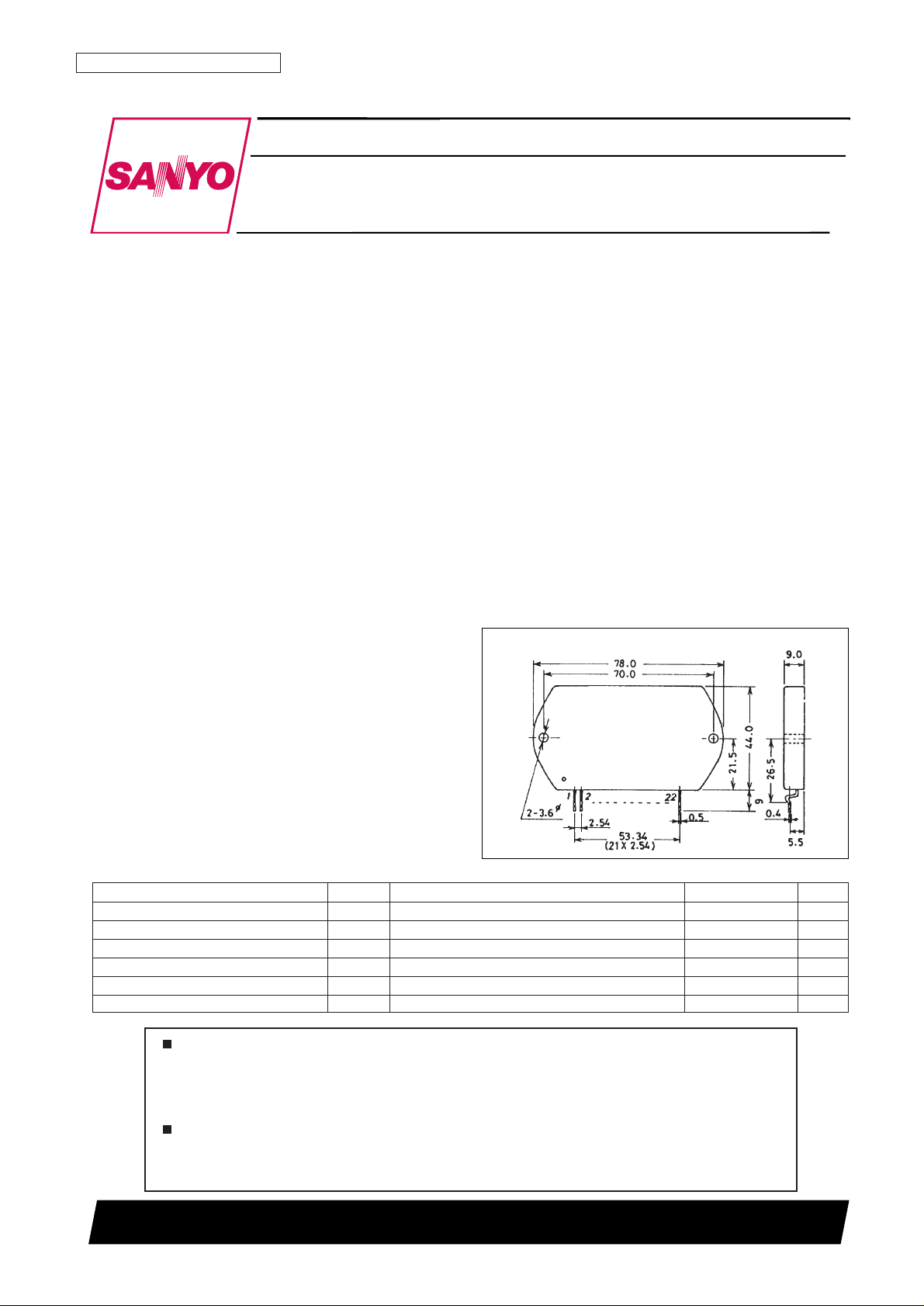
Package Dimensions
unit: mm
4086A
Specifications
Absolute Maximum Ratings at Ta = 25°C
Parameter Symbol Conditions Ratings Unit
Maximum supply voltage V
CC
max ±44 V
Maximum collector current I
C
Tr8, 10, 18, 20, 28, 30 +6.0 A
Thermal resistance θj-c Tr8, 10, 18, 20, 28, 30 (per transistor) 2.1 °C/W
Junction temperature Tj 150 °C
Operating substrate temperature Tc 125 °C
Storage temperature Tstg –30 to +125 °C
[STK392-020]
Page 2

Operating Characteristics at Ta = 25°C, Rg = 50 Ω
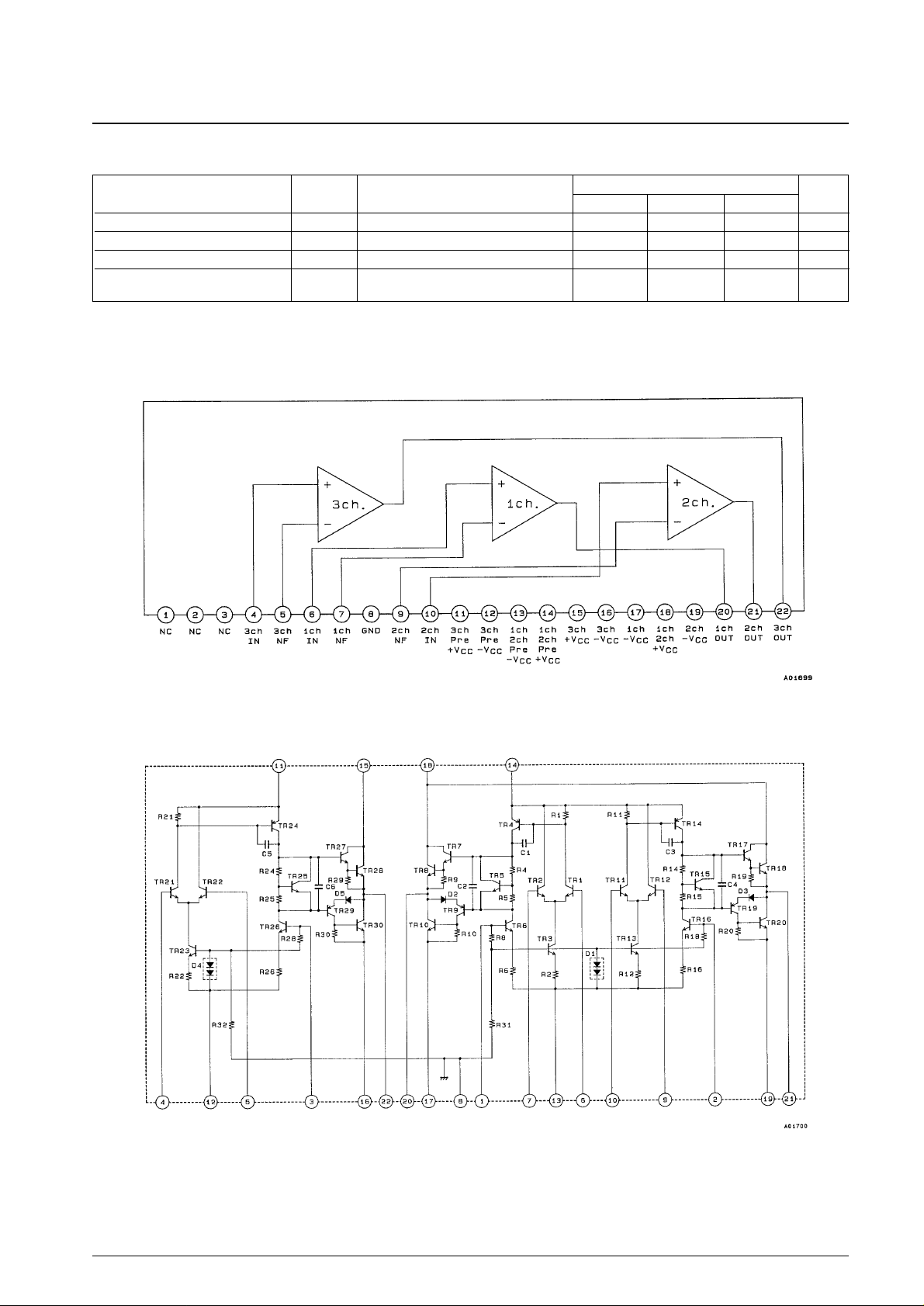
Equivalent Circuit Block Diagram
Internal Equivalent Circuit
No. 4688-2/8
STK392-020
Parameter Symbol Conditions
Ratings
Unit
min typ max
Output noise voltage V
NO
VCC= ±35 V 0.2 mVrms
Quiescent current I
CCO
VCC= ±35 V 30 90 150 mA
Neutral voltage V
N
VCC= ±35 V –50 0 +50 mV
Output delay time t
D
VCC= ±35 V, f = 15.75 kHz;
1.0 µs
Triangle wave input, V
OUT
= 1.5 Vp-p
Page 3

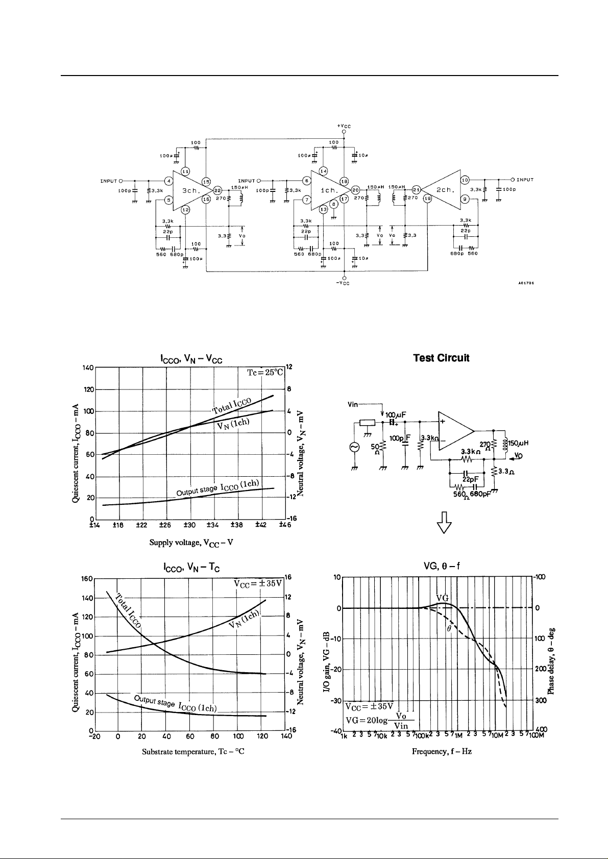
Test Circuit
No. 4688-3/8
STK392-020
Unit (resistance: Ω, capacitance: F)
Vo: Connect to VTVM when measuring V
NO
Connect to a DC volt meter when measuring V
N
Connect to the oscilloscope when measuring t
D
Page 4

No. 4688-4/8
STK392-020
Page 5

Thermal Design
1. Tj max, Tc max, and θj-c
Tj max, Tc max, and θj-c are stipulated in the maximum ratings as required parameters for thermal design.
• Tj max (junction temperature)
Tj max is a parameter that is due to the physical structure of the internal devices. Since devices will be degraded or
destroyed if Tj exceeds this value, the design must not allow this value to be exceeded.
• Tc max (operating substrate temperature)
Tc max is a parameter that arises from the internal devices, the materials used, and the circuit design. It is
determined based on comprehensive considerations, including reliability. Devices are not guaranteed if they are
operated with Tc exceeding this value.
• θj-c (thermal resistance)
θj-c differs for each device in the design, and is stipulated in the maximum ratings since it is required to calculate
Tj for the major devices in the design.
Note that Tj and Tc are independent parameters that depend on the operating conditions, and the thermal design must
fulfill the maximum ratings of both these parameters.
2. Approaches to Thermal Design
Let Pd be the IC case internal operating power dissipation, and Pc be the power dissipation per power transistor. The
required heat sink thermal resistance (θc-a) for this case internal power dissipation (Pd) can be derived as follows:
Condition 1: Taking Ta to be the end product guaranteed ambient temperature, the IC case temperature Tc must not
exceed 125°C.
Pd × θc-a + Ta < 125°C (Tc max)................................①
Condition 2: The power transistor junction temperature must not exceed 150°C.
Pd × θc-a + Pc × θj-c + Ta < 150°C (Tj max)..............②
Where θj-c is the thermal resistance per power transistor.
The thermal design must fulfill these above conditions.
3. Design Procedure
The figure at right shows a model of the STK392-020 channel 1 circuit.
Taking the Pd’s of each channel to be Pd1 (channel 1), Pd2 (channel 2)
and Pd3 (channel 3), the total Pd max can be determined as:
Pd max = Pd1 max + Pd2 max + Pd3 max
That is, condition ① gives:
θc-a < ..............................................③
which allows the required heat sink thermal resistance to be derived.
(Here, Tc max is taken to be 125°C.)
Also, taking the power dissipation per power transistor for each channel
to be Pc, the transistor junction temperature Tj will be:
Tj = Pd max × θc-a + Ta + Pc + θj-c............................④
and this can be used to confirm that Tj does not exceed Tj max (150°C).
At this point, if Tj exceeds 150°C in the design, Tc must be lowered by lowering the heat sink thermal resistance
θc-a so that Tj does not exceed 150°C.
Tc max – Ta max
Pd max
No. 4688-5/8
STK392-020
STK392-020 Circuit Model (channel 1)
Page 6

4. Thermal Design Example
Take the following to be the worst operating conditions for the STK392-020.
VCCH = ±35 V
VCCL = ±25 V
Output coil, LY= 150 µH, RY= 0 Ω
Current detection resistor RNF= 3.3 Ω
Ip-o max = 0.4 Ap-o (Ip-p = 0.8 A), Sawtooth waveform input
Io(DC) max = 0.4 A DC input
All three channels operating under the same conditions
Ta max = 60°C (unit internal temperature)
From figures 1 and 2, it can be seen that the Pd1 for channel 1 is:
(a) For a sawtooth wave input: Pd1 max = 4.8 W (AC)
(b) For a DC input: Pd1 max = 9.5 W (DC)
This shows that Pd1 max AC < Pd1 max DC, i.e. that Pd1 is larger for a DC input.
Also, considering Pc for the output transistors gives:
(a) For a sawtooth wave (AC) input:Pc = 1/2 Pd1
(b) For a DC input: Pc = Pd1 (Since the power concentrates in the transistor on one side.)
Therefore, the DC input Pc for the output transistors is larger.
Accordingly, the remainder of the thermal design is based on the DC input case.
Here we ignore the power dissipation in the early stages.
When: Pd1 max = Pd2 max = Pd3 max = 9.5 W, then the Pd max (total for three channels) will be:
Pd max = Pd1 max × 3 = 28.5 W
θc-a = = = 2.28°C/W
This means that if a 2 mm thick Al plate (with an unfinished surface) is used as the heat sink, then figure 3 shows
that the following area S is required.
S = 625 cm2(25 × 25 cm)
Also, from formula ④, we see that the power transistor junction temperature Tj at this time will be:
Tj = Pd max ×θc-a + Ta + Pc max ×θj-c
= 28.5 × 2.28 + 60 + 9.5 × 2.1
= 145°C
This is a 5°C derating from the required 150°C Tj max.
(Addendum) To be precise, the power dissipated in the early stage circuits (transistor, resistors, etc.) should also be
taken into consideration.
Figure 1: Sawtooth wave input (AC) Ip-o – Pd1
Figure 2: DC input Io(DC) – Pd1
Figure 3: Aluminum plate thermal resistance characteristics
125 – 60
28.5
Tc max – Ta
Pd max
No. 4688-6/8
STK392-020
Page 7

No. 4688-7/8
STK392-020
Sawtooth wave input DC input
Page 8

PS No. 4688-8/8
STK392-020
This catalog provides information as of December, 1998. Specifications and information herein are
subject to change without notice.
Specifications of any and all SANYO products described or contained herein stipulate the performance,
characteristics, and functions of the described products in the independent state, and are not guarantees
of the performance, characteristics, and functions of the described products as mounted in the customer’s
products or equipment. To verify symptoms and states that cannot be evaluated in an independent device,
the customer should always evaluate and test devices mounted in the customer’s products or equipment.
SANYO Electric Co., Ltd. strives to supply high-quality high-reliability products. However, any and all
semiconductor products fail with some probability. It is possible that these probabilistic failures could
give rise to accidents or events that could endanger human lives, that could give rise to smoke or fire,
or that could cause damage to other property. When designing equipment, adopt safety measures so
that these kinds of accidents or events cannot occur. Such measures include but are not limited to protective
circuits and error prevention circuits for safe design, redundant design, and structural design.
In the event that any or all SANYO products (including technical data, services) described or contained
herein are controlled under any of applicable local export control laws and regulations, such products must
not be exported without obtaining the export license from the authorities concerned in accordance with the
above law.
No part of this publication may be reproduced or transmitted in any form or by any means, electronic or
mechanical, including photocopying and recording, or any information storage or retrieval system,
or otherwise, without the prior written permission of SANYO Electric Co., Ltd.
Any and all information described or contained herein are subject to change without notice due to
product/technology improvement, etc. When designing equipment, refer to the “Delivery Specification”
for the SANYO product that you intend to use.
Information (including circuit diagrams and circuit parameters) herein is for example only; it is not
guaranteed for volume production. SANYO believes information herein is accurate and reliable, but
no guarantees are made or implied regarding its use or any infringements of intellectual property rights
or other rights of third parties.
 Loading...