

Page 1
Any and all SANYO products described or contained herein do not have specifications that can handle
applications that require extremely high levels of reliability, such as life-support systems, aircraft’s
control systems, or other applications whose failure can be reasonably expected to result in serious
physical and/or material damage. Consult with your SANYO representative nearest you before using
any SANYO products described or contained herein in such applications.
SANYO assumes no responsibility for equipment failures that result from using products at values that
exceed, even momentarily, rated values (such as maximum ratings, operating condition ranges,or other
parameters) listed in products specifications of any and all SANYO products described or contained
herein.
Thick Film Hybrid IC
2-Channel Convergence Correction Circuit
(I
C
max = 6A)
Ordering number:ENN5169
STK391-020
SANYO Electric Co.,Ltd. Semiconductor Company
TOKYO OFFICE Tokyo Bldg., 1-10, 1 Chome, Ueno, Taito-ku, TOKYO, 110-8534 JAPAN
Overview
The STK391-020 is a conver gence correction circuit IC for
video projectors. It incorporates two output amplifiers in a
single package, making possible the construction of CRT
horizontal and vertical convergence correction output circuits for each of the RGB colors using ust three hybrid ICs.
Applications
• V ideo projectors
Features
• 2 output amplifier circuits in a single package
• High maximum supply voltage (VCC max = ±44V)
• Low thermal resistance (θj-c=2.7°C/W)
• High temperature stability (good idling current temperature compensation)
• Low correction coil inductance for improved oscillator
stability (up to fH = 64kHz)
• Pin compatible with the STK4274 for easy replacement
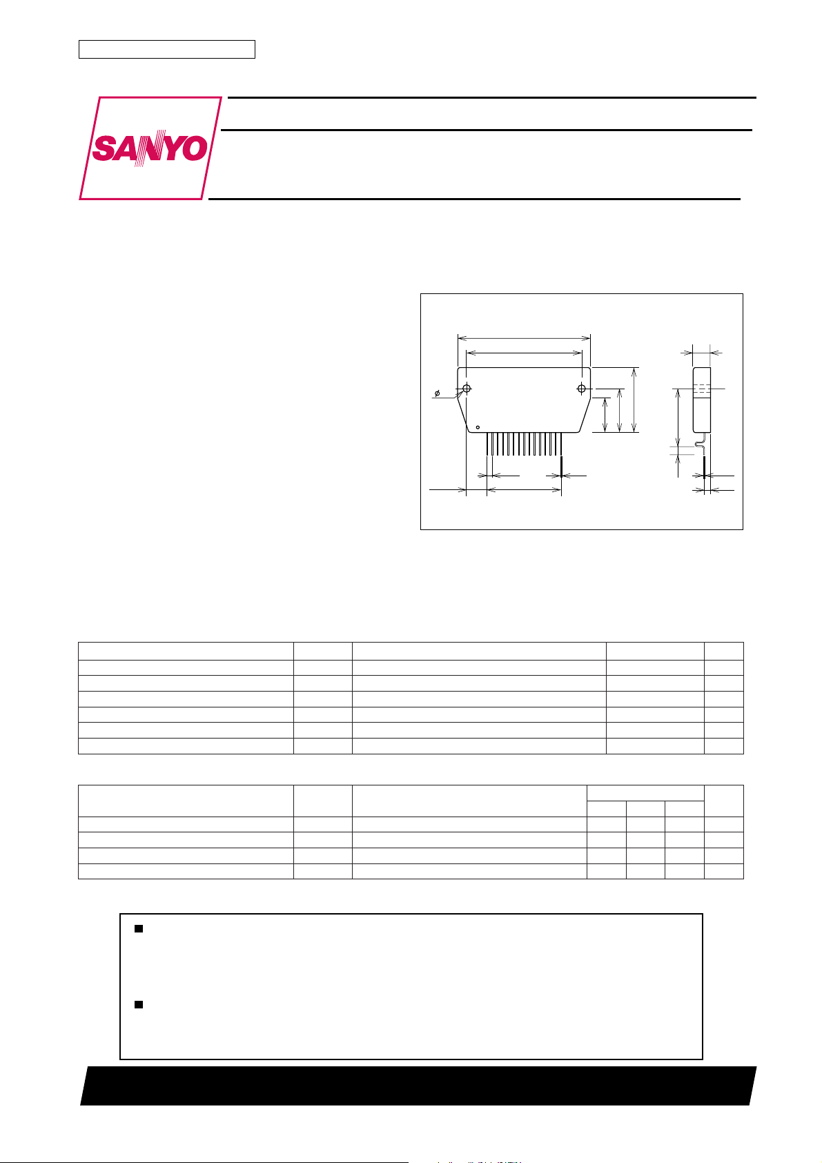
Package Dimensions
unit:mm
4062
3.6
1
(10.02)
64.0
55.6
2.54
14×2.54=35.56
[STK391-020]
16.5
15
0.5
21.0
31.0
8.5
4.0 28.0
SANYO : SIP15
0.4
2.9
Specifications
Maximum Ratings at Ta = 25˚C
retemaraPlobmySsnoitidnoCsgnitaRtinU
egatlovylppusmumixaMV
tnerrucrotcellocmumixaMI
ecnatsiserlamrehT
erutarepmetnoitcnuJjT 051
erutarepmetgnitarepOcT 501
erutarepmetegarotSgtsT 501+ot03–
Operating Characteristics at Ta = 25˚C, Rg=50Ω, VCC=±24V
retemaraPlobmySsnoitidnoC
egatlovesiontuptuOV
tnerructnecseiuQI
egatlovlartueNV
emityaledtuptuOt
xam 44±V
CC
C
θ c-j
ON
OCC
N
D
22,02,11,9rT 0.6A
)rotsisnartrep(22,02,11,9rT 7.2
V,tupnievawralugnairt,zHk57.51=f
p-pV5.1=1sµ
TUO
92099TH (KT)/80995HA (ID) No.5169–1/6
sgnitaR
nimpytxam
2.0smrVm
0204Am
05–005+Vm
˚C/W
˚C
˚C
˚C
tinU
Page 2
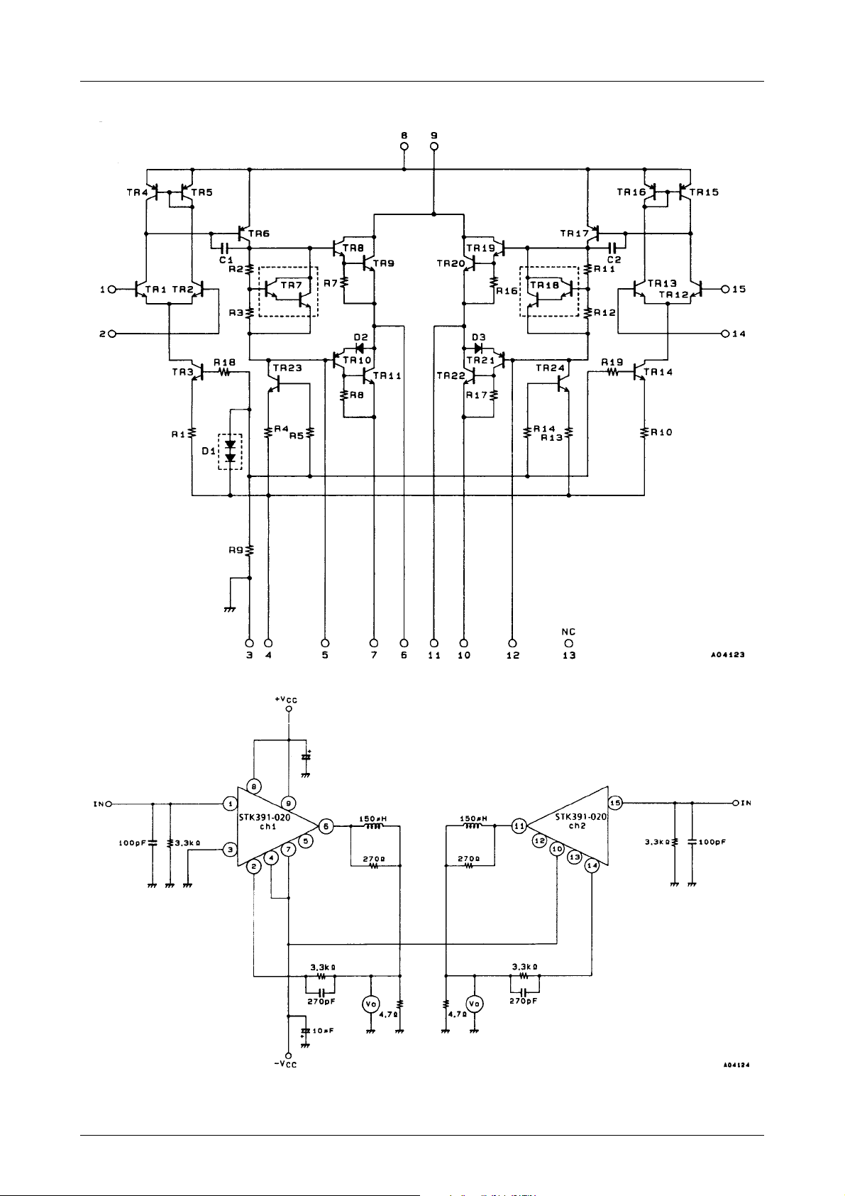
Equivalent Circuit
STK391-020
Test Circuit
Vo : VNO is measured by connecting a VTVM.
VN is measured by connecting a DC voltmeter.
tD is measured by connecting an oscilloscope.
No.5169–2/6
Page 3

STK391-020
No.5169–3/6
Page 4

STK391-020
Maximum Ratings
Tj max, Tc max, θj-c
The heatsink design is determined by the maximum ratings of several key parameters–Tj max, Tc max and θj-c.
• Tj max (junction temperature)
Tj max is dependent on the physical structure of each functional element. A junction temperature exceeding this r ating can lead to device deterioration and breakdown, so
the design must not exceed this rating.
• Tc max (operating substrate temperature)
Tc max is dependent on the materials used within an element and on the circuit design, and should be selected on
the basis of reliability. Operation exceeding this value is
not guaranteed.
• θj-c (thermal resistance)
θj-c is dependent on the heatsink design, which can vary
greatly. the heatsink necessary is determined by calcula-
tion using the maximum rating for Tj.
As Tj and Tc operating conditions are independent, the
heatsink must be designed to satisfy the maximum ratings
for both parameters.
Heatsink Design Considerations
In the expressions below Pd represents the operating IC
substrate internal power dissipation and Pc represents the
power dissipation per transistor. The heatsink thermal resistance, θc-a, required to dissipate the total power dissipation, Pd, is determined as follows :
The power dissipation, Pd, is the sum of channel 1, Pd1,
and channel 2, Pd2, power dissipations.
Pd max=Pd1 max+Pd2 max
Therefore, form equation (1),
θc-a< ................................ (3)
the necessary heatsink resistance is determined (note that
Tc max=105°C)
The power dissipation per power transistor per channel, Pc,
is related to the transistor junction temperature by the following equation.
Tj=Pd max×θc-a+Ta+Pc×θj-c ............................ (4)
where Tj cannot exceed Tj max=105°C. Therfore, in order
to maintain Tj below 150°C, a lower heatsink thermal resistance, θc-a, is necessary to lower Tc.
Heatsink Design Example
This example assumes the following worst-case conditions–
VCCH=±35V, VCCL=±25V, output coil LY=80µH and
RY=0Ω, current detector resistance RNF=4.7Ω, Ip-o
max=0.6Ap-o (Ip-o (Ip-p=1.2A) sawtooth wave input, Io
(DC) max=0.6A DC input, both chanels operating, Ta
max=60°C (guaranteed maximum).
Tc max – Ta max
Pd max
Condition 1: IC substrate temperature not to exceed 105°C
Pd×θc-a+Ta<105°C (Tc max) ............................ (1)
Where Ta is the guaranteed maximum ambient temperature.
Condition 2: Power transistor junction temperature, Tj, not
to exceed 150°C
Pd×θc-a+Pc×θj-c+Ta<150°C (Tj max) .............. (2)
Where θj-c is the power transistor thermal resistance per
transistor. Therefore, the heatsink design m ust satisfy both
these expression.
Design Process
A model circuit for a single channel in the STK319-020 is
shown below.
The channel1 power dissipation, Pd1, is given from Figures 1 and 2.
• Pd1 max=7.0W (AC) with sawtooth wave input
• Pd1 max=13.2W (DC) with DC input
As Pd1 max (AC) < Pd1 max (DC), the power dissipation
is greater with DC input. Also, lokking at the output transistor dissipation, Pc,
• Pc=0.5Pd1 with sawtooth wave input
• Pc=Pd1 with DC input (one side transistor continuously
ON)
the power dissipation is also higher with DC input. Accordingly, the heatsink design example below assumes DC
input. The power dissipation in the predriver stage is ignored.
As Pd1 max=Pd2 max+13.2W, Pd max (both channels) is
given by.
Pd max=Pd1 max+Pd2 max=26.4W
From equation (3) with Ta=60°C,
θc-a= = = ........ 1.70°C/W
For a 2mm aluminum heatsink with no surface coating, the
necessary surface area, S, is given from Figure 3.
Tc max – Ta
Pd max
105–60
26.4
S=780cm2 (28cm×28cm)
No.5169–4/6
Page 5

STK391-020
Also from equation (4), the output stage power transistor
jucntion temperature is given by
Tj =Pd max×θc-a+Ta+Pc max×θj-c
=26.4×1.7+60+13.2×2.7
=140.5°C
which provides a 9.5°C derating below Tj max=150°C.
However, an allowance for the predri v er stage power dissipation (transistors, resistors, etc.) should also be included
in the substrate internal power dissipation, Pd.
No.5169–5/6
Page 6

STK391-020
Specifications of any and all SANYO products described or contained herein stipulate the performance,
characteristics, and functions of the described products in the independent state, and are not guarantees
of the performance, characteristics, and functions of the described products as mounted in the customer's
products or equipment. To verify symptoms and states that cannot be evaluated in an independent device,
the customer should always evaluate and test devices mounted in the customer's products or equipment.
SANYO Electric Co., Ltd. strives to supply high-quality high-reliability products. However, any and all
semiconductor products fail with some probability. It is possible that these probabilistic failures could
give rise to accidents or events that could endanger human lives, that could give rise to smoke or fire,
or that could cause damage to other property. When designing equipment, adopt safety measures so
that these kinds of accidents or events cannot occur. Such measures include but are not limited to protective
circuits and error prevention circuits for safe design, redundant design, and structural design.
In the event that any or all SANYO products(including technical data,services) described or
contained herein are controlled under any of applicable local export control laws and regulations,
such products must not be exported without obtaining the export license from the authorities
concerned in accordance with the above law.
No part of this publication may be reproduced or transmitted in any form or by any means, electronic or
mechanical, including photocopying and recording, or any information storage or retrieval system,
or otherwise, without the prior written permission of SANYO Electric Co. , Ltd.
Any and all information described or contained herein are subject to change without notice due to
product/technology improvement, etc. When designing equipment, refer to the "Delivery Specification"
for the SANYO product that you intend to use.
Information (including circuit diagrams and circuit parameters) herein is for example only ; it is not
guaranteed for volume production. SANYO believes information herein is accurate and reliable, but
no guarantees are made or implied regarding its use or any infringements of intellectual property rights
or other rights of third parties.
This catalog provides information as of September, 1999. Specifications and information herein are
subject to change without notice.
PS No.5169–6/6
 Loading...