

SANYO LC78631E Datasheet
Overview
The LC78631E is a compact disc D/A signal-processing
LSI for CD-ROM drives that provides a variable clock
error correction (VCEC) mode. The LC78631E
demodulates the EFM signal from the optical pickup and
performs de-interleaving, error detection, error correction,
digital filtering, and other processing. The LC78631E
includes an on-chip 1-bit D/A converter, and executes
commands sent from a control microprocessor.
Features
• VCEC support
• Built-in PLL circuit for EFM detection (supports 4×
playback)
• Built-in PLL for variable pitch playback (±13%)
• 18KB RAM on chip
• Error detection and correction (corrects two errors in C1
and four errors in C2)
• Frame jitter margin: ±8 frames
• Frame synchronization signal detection, protection, and
insertion
• Dual interpolation adopted in the interpolation circuit.
• EFM data demodulation
• Subcode demodulation
• Zero-cross muting adopted
• Servo command interface
• 2fs digital filter
• Digital de-emphasis
• Built-in independent left- and right-channel digital
attenuators (239 attenuation steps)
• Supports the bilingual function
• Left/right swap function
• Built-in 1-bit D/A converter (third-order ∆∑ noise
shaper, PWM output)
• Built-in digital output circuit
• CLV servo
• Arbitrary track jumping (of up to 255 tracks)
• Variable sled voltage (four levels)
• Six extended I/O ports and 2 extended output ports
• Built-in oscillator circuit using an external 16.9344 MHz
or 33.8688 MHz (for 4× playback) element
• Supply voltage: 3.6 to 5.5 V (4.75 to 5.5 V for 4×
playback mode)
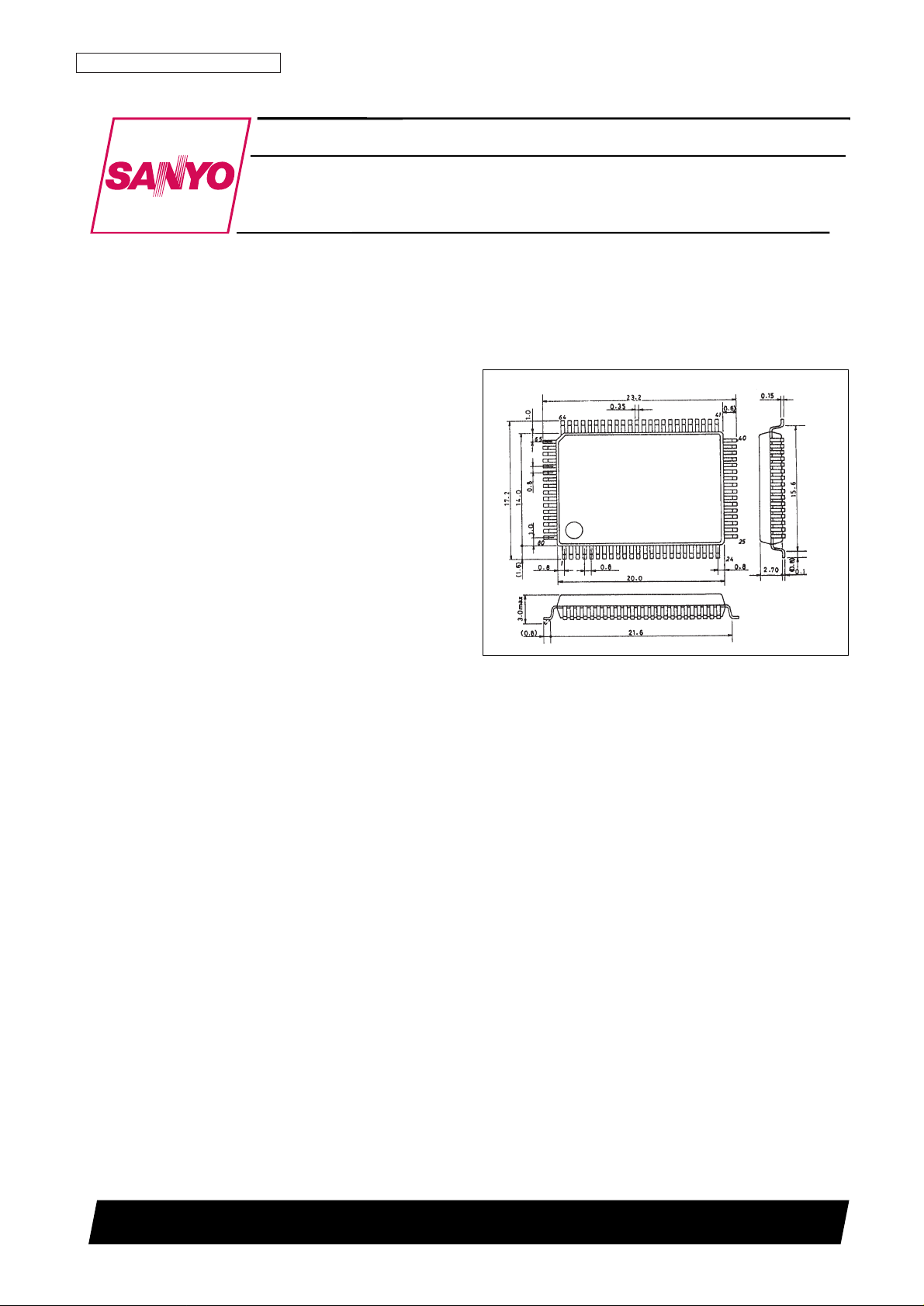
Package Dimensions
unit: mm
3174-QFP80E
CMOS LSI
62096HA (OT) No. 5342-1/34
SANYO: QFP80E
[LC78631E]
SANYO Electric Co.,Ltd. Semiconductor Bussiness Headquarters
TOKYO OFFICE Tokyo Bldg., 1-10, 1 Chome, Ueno, Taito-ku, TOKYO, 110 JAPAN
Compact Disk Player DSP
LC78631E
Ordering number : EN 5342
No. 5342-2/34
LC78631E
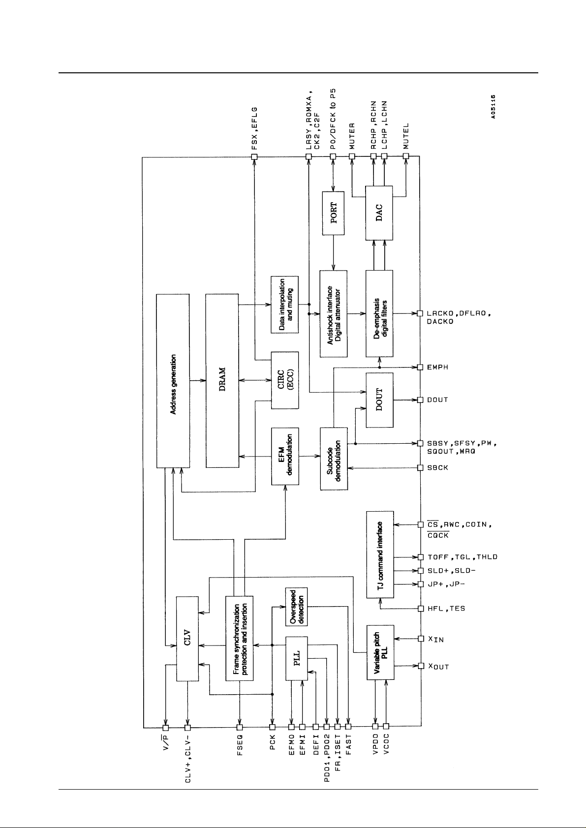
Equivalent Circuit Block Diagram
No. 5342-3/34
LC78631E
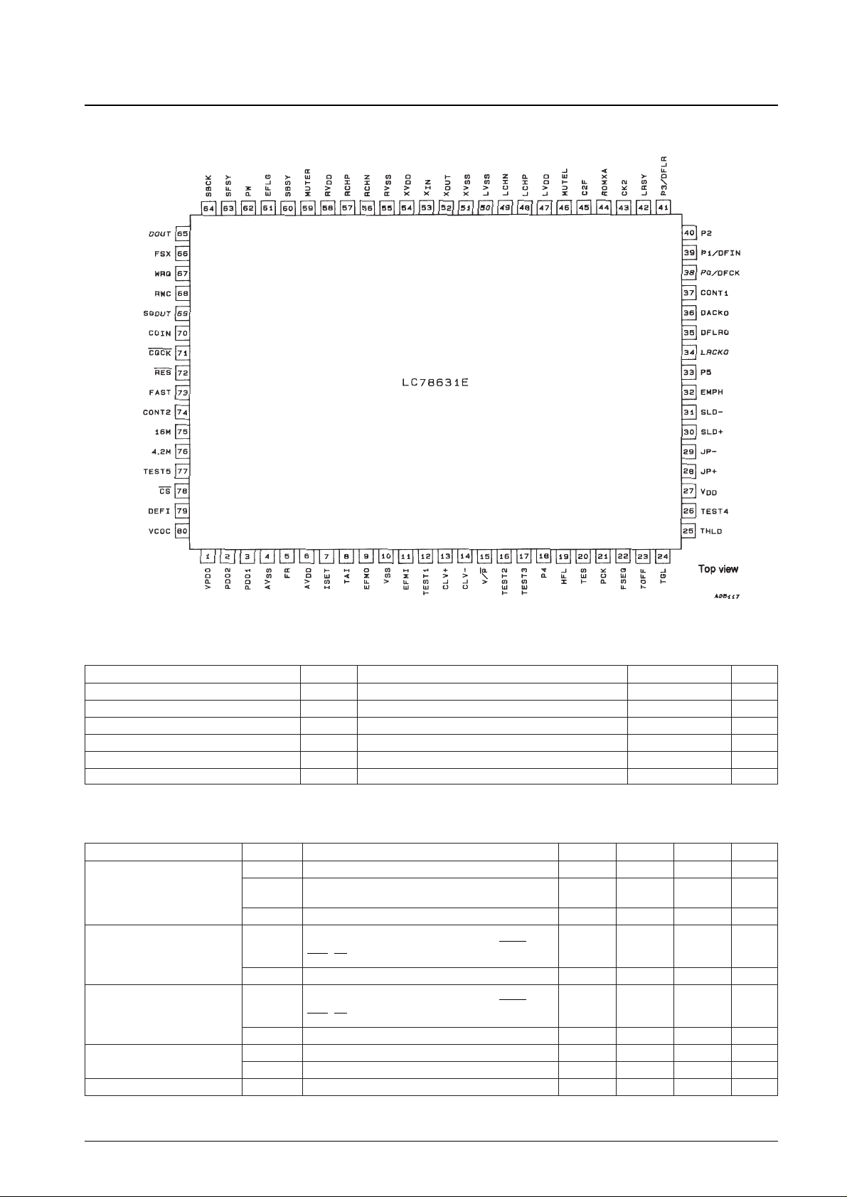
Pin Assignment
Absolute Maximum Ratings at Ta = 25°C, VSS= 0 V
Allowable Operating Ranges at Ta = 25°C, VSS= 0 V
Parameter Symbol Conditions Ratings Unit
Maximum supply voltage V
DD
max –0.3 to +7.0 V
Input voltage V
IN
–0.3 to VDD+ 0.3 V
Output voltage V
OUT
–0.3 to VDD+ 0.3 V
Allowable power dissipation Pd max 470 mW
Operating temperature Topr –30 to +75 °C
Storage temperature Tstg –40 to +125 °C
Parameter Symbol Conditions min typ max Unit
V
DD
1 VDD, AVDD, XVDD, LVDD, RV
DD
3.6 5.0 5.5 V
Supply voltage
V
DD
2
V
DD
, AVDD, XVDD, LVDD, RVDD:
4.5 5.0 5.5 V
For variable-pitch playback
V
DD
3 VDD, AVDD, XVDD, LVDD, RVDD: For 4× playback 4.75 5.0 5.5 V
TEST1 to TEST5, TAI, HFL, TES, P0/DFCK, P1/DFIN,
Input high-level voltage
VIH1 P2, P3/DFLR, P4, P5, SBCK, RWC, COIN, CQCK, 0.7 V
DD
V
DD
V
RES, CS, X
IN
, DEFI
V
IH
2 EFMI 0.6 V
DD
V
DD
V
TEST1 to TEST5, TAI, HFL, TES, P0/DFCK, P1/DFIN,
Input low-level voltage
VIL1 P2, P3/DFLR, P4, P5, SBCK, RWC, COIN, CQCK 0 0.3 V
DD
V
RES, CS, X
IN
, DEFI
V
IL
2 EFMI 0 0.4 V
DD
V
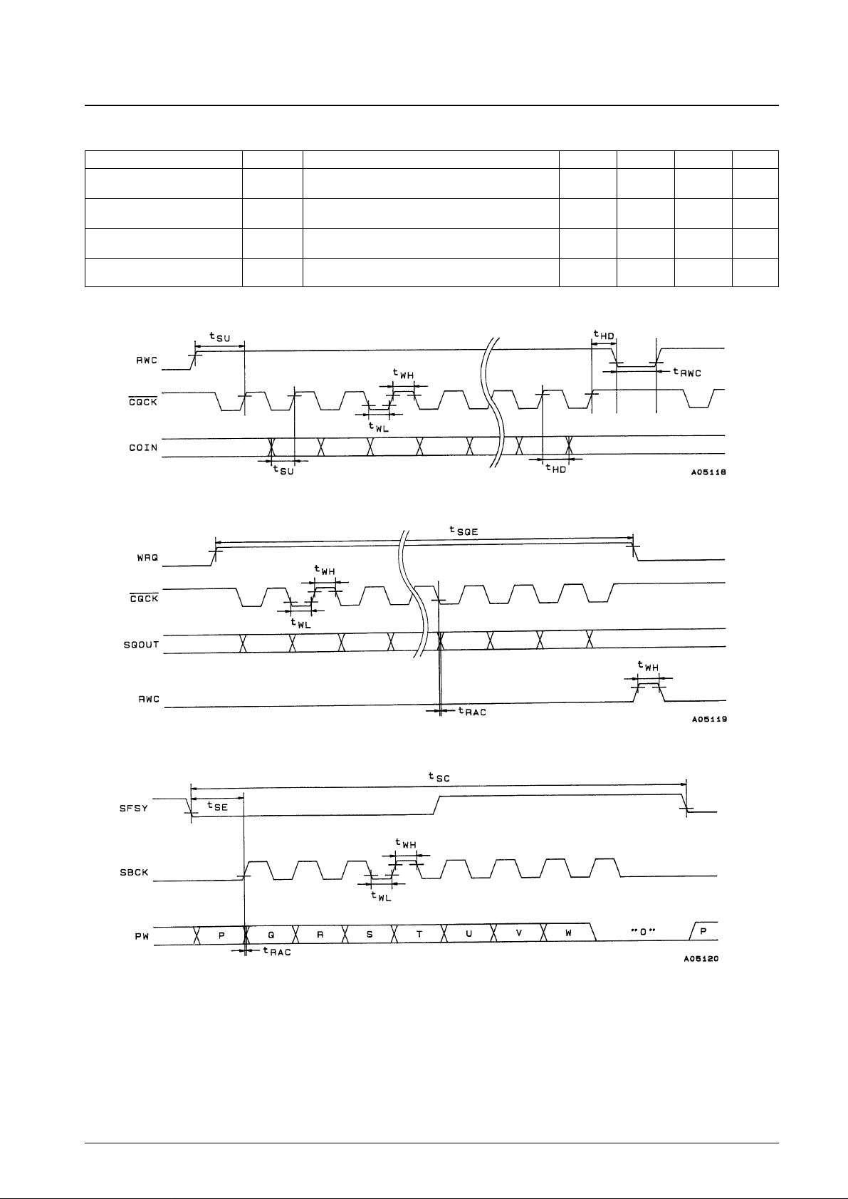
Data setup time
t
SU
COIN, RWC: Figures 1 and 4 400 ns
t
PRS
RWC: Figure 4 100 ns
Data hold time t
HD
COIN, RWC: Figures 1 and 4 400 ns
Continued on next page.
No. 5342-4/34
LC78631E
Continued from preceding page.
Parameter Symbol Conditions min typ max Unit
High-level clock pulse width t
WH
SBCK, CQCK: Figures 1, 2, 3, and 4 400 ns
Low-level clock pulse width t
WL
SBCK, CQCK: Figures 1, 2, 3, and 4 400 ns
Data read access time t
RAC
SQOUT, PW: Figures 2, 3, and 4 0 400 ns
Command transfer time t
RWC
RWC: Figures 1 and 4 1000 ns
Subcode Q read enable time t
SQE
WRQ: Figure 2, with no RWC signal 11.2 ms
Subcode read cycle t
SC
SFSY: Figure 3 136 µs
Subcode read enable t
SE
SFSY: Figure 3 400 ns
Port output delay time t
PD
CONT1, CONT2, P0 to P5: Figure 5 1200 ns
Input level
V
EI
EFMI 1.0 Vp-p
V
XI
XIN: Capacitance coupled input 1.0 Vp-p
Parameter Symbol Conditions min typ max Unit
Current drain I
DD
Normal-speed playback 30 mA
I
IH
1
EFMI, HFL, TES, SBCK, RWC, COIN, CQCK, RES,
5 µA
Input high-level current
DEFI: V
IN
= 5 V
I
IH
2 TAI, TEST1 to TEST5, CS: VIN= 5 V 25 75 µA
Input low-level current I
IL
TAI, EFMI, HFL, TES, SBCK, RWC, COIN, CQCK, RES,
–5 µA
TEST1 to TEST5, CS, DEFI: V
IN
= 0 V
EFMO, CLV
+
, CLV–, V/P, PCK, FSEQ, TOFF, TGL,
V
OH
1 THLD, JP+, JP–, EMPH, EFLG, FSX, FAST: 4 V
I
OH
= –1 mA
MUTEL, MUTER, LRCKO, DFLRO, DACKO, P0/DFCK,
V
OH
2
P1/DFIN, P2, P3/DFLR, P4, P5, LRSY, CK2, ROMXA,
4 V
Output high-level voltage C2F, SBSY, PW, SFSY, WRQ, SQOUT, 16M, 4.2M,
CONT1, CONT2: I
OH
= –0.5 mA
V
OH
3 VPDO: IOH= –1 mA 4.5 V
V
OH
4 DOUT: IOH= –12 mA 4.5 V
V
OH
5 LCHP, RCHP, LCHN, RCHN: IOH= –1 mA 3.0 4.5 V
EFMO, CLV
+
, CLV–, V/P, PCK, FSEQ, TOFF, TGL,
V
OL
1 THLD, JP+, JP–, EMPH, EFLG, FSX, FAST: 1 V
I
OL
= 1 mA
MUTEL, MUTER, LRCKO, DFLRO, DACKO, P0/DFCK,
V
OL
2
P1/DFIN, P2, P3/DFLR, P4, P5, LRSY, CK2, ROMXA,
0.4 V
Output low-level voltage C2F, SBSY, PW, SFSY, WRQ, SQOUT, 16M, 4.2M,
CONT1, CONT2: I
OL
= 2 mA
V
OL
3 VPDO: IOL= 1 mA 0.5 V
V
OL
4 DOUT: IOL= 12 mA 0.5 V
V
OL
5 LCHP, RCHP, LCHN, RCHN: IOL= 1 mA 0.5 2.0 V
IOFF1
PDO1, PDO2, VPDO, P0/DFCK, P1/DFIN,
5 µA
Output off leakage current
P2, P3/DFLR, P4, P5: V
OUT
= 5 V
I
OFF
2
PDO1, PDO2, VPDO, P0/DFCK, P1/DFIN,
–5 µA
P2, P3/DFLR, P4, P5: V
OUT
= 0 V
Charge pump output current
I
PDOH
PDO1, PDO2: R
ISET
= 68 kΩ –96 –80 –64 µA
I
PDOL
PDO1, PDO2: R
ISET
= 68 kΩ 64 80 96 µA
V
SLD
1 1.0 1.25 1.5 V
Sled output voltage
V
SLD
2 2.25 2.5 2.75 V
V
SLD
3 3.5 3.75 4.0 V
V
SLD
4 4.75 V
Note: Due to the structure of this IC, the identical voltage must be applied to all power-supply pins.
Electrical Characteristics at Ta = 25°C, VDD= 5 V, VSS= 0 V
No. 5342-5/34
LC78631E
D/A Converter Analog Characteristics at Ta = 25°C, VDD= 5 V, VSS= 0 V
Note: Measured in normal-speed playback mode in a Sanyo 1-bit D/A converter block reference circuit, with the digital attenuator set to EE (hexadecimal).
Figure 1 Command Input
Figure 2 Subcode Q Output
Figure 3 Subcode Output
Parameter Symbol Conditions min typ max Unit
Total harmonic distortion THD + N
LCHP, LCHN, RCHP, RCHN; 1 kHz: 0 dB input,
0.006 %
using a 20-kHz low-pass filter (AD725D built in)
Dynamic range DR
LCHP, LCHN, RCHP, RCHN; 1 kHz: –60 dB input, using
90 dB
the 20-kHz low-pass filter (A filter (AD725D built in))
Signal-to-noise ratio S/N
LCHP, LCHN, RCHP, RCHN; 1 kHz: 0 dB input, using
98 100 dB
the 20-kHz low-pass filter (A filter (AD725D built in))
Crosstalk CT
LCHP, LCHN, RCHP, RCHN; 1 kHz: 0 dB input,
96 98 dB
using a 20-kHz low-pass filter (AD725D built in)
No. 5342-6/34
LC78631E
Figure 4 General-Purpose Port Read
Figure 5 General-Purpose Port Output
No. 5342-7/34
LC78631E
One-Bit D/A Converter Output Block Reference Circuit
No. 5342-8/34
LC78631E
Pin Functions
Note: Of the general-purpose I/O ports, any unused input ports must be connected to 0 V, or set to be output ports.
Pin No. Symbol I/O Function
1 VPDO O Variable pitch PLL charge pump output. Must be left open if unused.
2 PDO2 O Double-speed and quad-speed mode playback PLL charge pump output. Must be left open if unused.
3 PDO1 O Normal-speed mode playback PLL charge pump output
4 AV
SS
Analog system ground. Must be connected to 0 V.
5 FR Built-in VCO frequency range setting resistor connection
6 AV
DD
Analog system power supply
7 ISET PDO1 and PDO2 output current setting resistor connection
8 TAI I Test input. A pull-down resistor is built in. Must be connected to 0 V.
9 EFMO O EFM signal output
10 V
SS
Digital system ground. Must be connected to 0 V.
11 EFMI I EFM signal input
12 TEST1 I Test input. A pull-down resistor is built in. Must be connected to 0 V.
13 CLV
+
O
Spindle servo control output. CLV
+
outputs a high level for acceleration, and CLV–outputs a high level for
14 CLV
–
O
deceleration.
15 V/P O
Rough servo/phase control automatic switching monitor output. A high-level output indicates rough servo, and a
low-level output indicates phase control.
16 TEST2 I Test input. A pull-down resistor is built in. Must be connected to 0 V.
17 TEST3 I Test input. A pull-down resistor is built in. Must be connected to 0 V.
18 P4 I/O I/O port
19 HFL I Track detection signal input. This is a Schmitt input.
20 TES I Tracking error signal input. This is a Schmitt input.
21 PCK O
EFM data playback bit clock monitor. Outputs 4.3218 MHz when the phase is locked in normal-speed mode
playback.
22 FSEQ O
Synchronization signal detection output. Outputs a high level when the synchronization signal detected from the
EFM signal matches the internally generated synchronization signal.
23 TOFF O Tracking off output
24 TGL O Tracking gain switching output. Increase the gain when this pin outputs a low level.
25 THLD O Tracking hold output
26 TEST4 I Test input. A pull-down resistor is built in. Must be connected to 0 V.
27 V
DD
Digital system power supply
28 JP
+
O
Track jump output. JP
+
outputs a high level both for acceleration during outward direction jumps and for
deceleration during inward direction jumps. JP
–
outputs a high level both for acceleration during inward direction
29 JP
–
O jumps and for deceleration during outward direction jumps.
30 SLD
+
O
Sled output. This pin can be set to 1 of 4 levels by commands sent from the system control microprocessor.
31 SLD
–
O
32 EMPH O De-emphasis monitor. A high level indicates that a disk requiring de-emphasis is being played.
33 P5 I/O I/O port
34 LRCKO O LR clock output
35 DFLRO O Digital filter outputs LR data output. The digital filter can be turned off with the DFOFF command.
36 DACKO O Bit clock output
37 CONT1 O Output port
38 P0/DFCK I/O I/O port. DF bit clock input in antishock mode.
39 P1/DFIN I/O I/O port. DF data input in antishock mode.
40 P2 I/O
I/O port. Used as the de-emphasis filter on/off switching pin in antishock mode. The de-emphasis filter is turned
on when this pin is high.
41 P3/DFLR I/O I/O port output or digital filter LR clock input (when anti-shock mode)
42 LRSY O LR clock output
43 CK2 O Bit clock output. The polarity can be inverted with the CK2CON command.
44 ROMXA O
ROMXA pins
Interpolated data output. Data that has not been interpolated can be output by issuing
the ROMXA command.
45 C2F O C2 flag output
46 MUTEL O Left channel mute output
47 LV
DD
Left channel power supply
48 LCHP O
One-bit D/A
Left channel P output
49 LCHN O
converter pins
Left channel N output
50 LV
SS
Left channel ground. Must be connected to 0V.
Continued on next page.
No. 5342-9/34
LC78631E
Note: Of the general-purpose I/O ports, any unused input ports must be connected to 0 V, or set to be output ports.
Pin No. Symbol I/O Function
51 XV
SS
Crystal oscillator ground. Must be connected to 0 V.
52 X
OUT
O
16.9344 MHz crystal oscillator connections. Use a 33.8688 MHz crystal oscillator for quad-speed playback.
53 X
IN
I
54 XV
DD
Crystal oscillator power supply
55 RV
SS
Right channel ground. Must be connected to 0 V.
56 RCHN O
One-bit D/A
Right channel N output
57 RCHP O
converter pins
Right channel P output
58 RV
DD
Right channel power supply
59 MUTER O Right channel mute output
60 SBSY O Subcode block synchronization signal output
61 EFLG O C1 and C2 error correction state monitor
62 PW O Subcode P, Q, R, S, T, U, V, and W output
63 SFSY O Subcode frame synchronization signal output. Falls when the subcode output goes to the standby state.
64 SBCK I Subcode readout clock input. This is a Schmitt input. This pin must be connected to 0 V if unused.
65 DOUT O Digital output
66 FSX O Outputs a 7.35 kHz synchronization signal generated by dividing the crystal oscillator frequency.
67 WRQ O Subcode Q output standby output
68 RWC I Read/write control input
69 SQOUT O Subcode Q output
70 COIN I Input for commands from the control microprocessor
71 CQCK I Command input acquisition clock. Also used as the SQOUT subcode readout clock input. This is a Schmitt input.
72 RES I Chip reset input. This pin must be set low temporarily when power is first applied.
73 FAST O Functions as the PCK frequency detection monitor output in VCEC mode.
74 CONT2 O Output port
75 16M O 16.9344 MHz output. 33.8688 MHz output in 4 × playback mode
76 4.2M O 4.2336 MHz output
77 TEST5 I Test input. A pull-down resistor is built in. Must be connected to 0 V.
78 CS I Chip select input. A pull-down resistor is built in. When control is not used, this pin must be connected to 0 V.
79 DEFI I Defect detection signal input. Must be connected to 0 V if unused.
80 VCOC I Variable pitch VCO control input. Must be connected to 0 V if unused.
Continued from preceding page.
No. 5342-10/34
LC78631E
CD D/A Converter Block Diagram
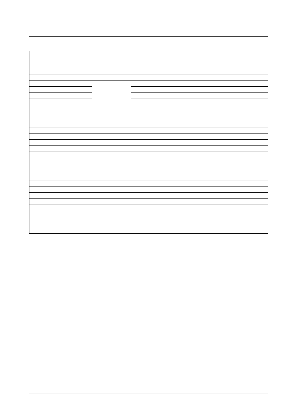
1. HF signal input circuit; Pin 11: EFMI, pin 9: EFMO, pin 79: DEFI, pin 13: CLV
+
When an HF signal is input to EFMI, the circuit slices it at an optimal
level to produce an EFM (NRZ) signal.
To deal with defects, if the DEFI pin (pin 79) goes high, the slice
level control output (EFMO, pin 9) goes to the high-impedance state
and the slice level is held. However, this function only operates when
CLV is in phase control mode, i.e., when the V/P pin (pin 15) is low.
This function can be formed by combining with the DEF pin on the
LA9230/40 Series LSI.
Note: If the EFMI and CLV+lines are placed too close together,
spurious radiation (induced noise) can degrade the error rate.
Therefore we recommend laying a ground or VDDshielding
line between these lines.
2. PLL clock reproduction circuit; Pin 2: PDO2, pin 3: PDO1, pin 5: FR, pin 7: ISET, pin 21: PCK
This block includes a VCO circuit, and a PLL
circuit is formed using external resistors and
capacitors. ISET is the charge pump reference
current, PDO1 and PDO2 are the loop filters, and
FR determines the VCO frequency range.
(Reference values)
R1 = 68 kΩ, C1 = 0.1 µF
R2 = 680 Ω, C2 = 0.1 µF
R3 = 680 Ω, C3 = 0.047 µF
R4 = 1.2 kΩ
3. Synchronization detection monitor; Pin 22: FSEQ
This pin outputs a high level when the frame sync (positive synchronizing signal), which is read by PCK from the
EFM signal, and the timing (the inserted synchronizing signal), which is generated by a counter, agree. Thus this pin
functions as a synchronization monitor. Note that it is held high during one frame.
No. 5342-11/34
LC78631E
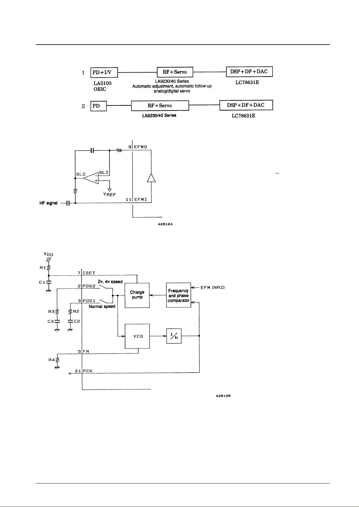
4. Command input
An external controller can execute LC78631E instructions by setting RWC high and inputting commands to COIN in
synchronization with the CQCK clock. Commands are executed on the fall of the RWC signal.
• Single-byte commands
• Two-byte commands
• Command noise reduction
This command can reduce the noise on the CQCK clock signal. While this is effective for noise pulses under
500 ns, the use of this function requires that the CQCK timings tWL, tWH, and tSU(see Figure 1 and 2) be set to
1 µs or longer.
5. CLV servo circuit
• CLV servo circuit; Pin 13: CLV+, pin 14: CLV–, pin 15: V/P
The CLV+signal causes the disc to accelerate in the forward direction, and CLV–causes the disc to decelerate. The
microcontroller can select one of four modes: accelerate, decelerate, CLV, and stop. The table below lists the states
of the CLV+and CLV–pins in each of these modes.
Note: The CLV servo control commands only set the TOFF pin low during CLV mode. That pin will be at the high
level at all other times. Thus controlling the TOFF pin with microcontroller commands is only possible in
CLV mode.
Code Command RES = low
$EF COMMAND INPUT NOISE REDUCTION MODE
$EE CLEAR THE ABOVE MODE
●●
Code Command RES = low
$04 DISC MOTOR START (accelerate)
$05 DISC MOTOR CLV (CLV)
$06 DISC MOTOR BRAKE (decelerate)
$07 DISC MOTOR STOP (stop)
●●
Mode CLV
+
CLV
–
Accelerate High Low
Decelerate Low High
CLV Pulse output Pulse output
Stop Low Low
 Loading...