


Ordering number : ENN6329
32400RM (OT) No. 6329-1/40
Overview
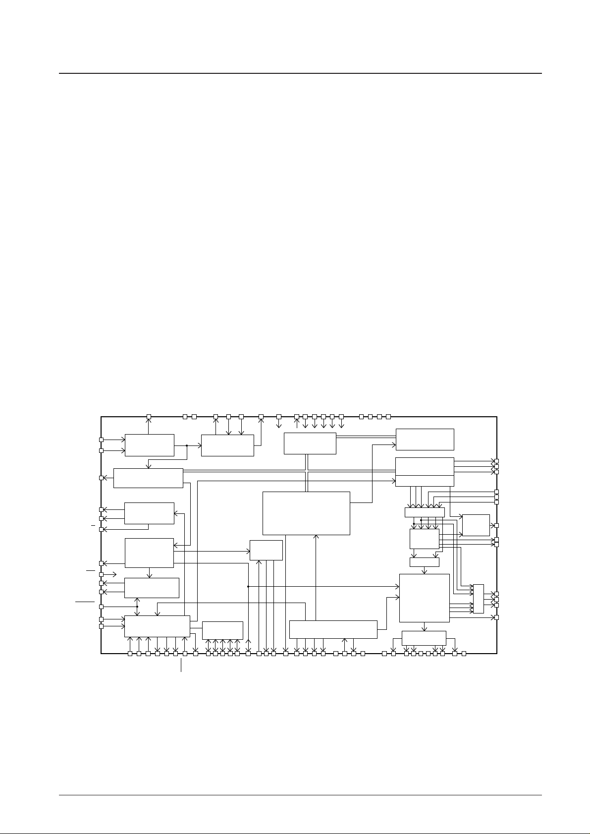
The LC78628E CMOS IC implements signal processing
and servo control for compact disc players, laser disc
players, CD-V, CD-I, and similar products. It provides
functions for demodulation of the EFM signal from the
optical pickup, deinterleaving, error detection and
correction, and processing servo system commands issued
by the system microprocessor. In addition to this basic CD
functionality, it also provides HDCD (High Definition
Compatible Digital) decoding functions and CD text
functions. It also includes a built-in EFM PLL circuit.
Functions
• Full decoding and playback for discs encoded with the
HDCD technique developed by Pacific Microsonics,
Inc.
• Slices the high-frequency input signal at an accurate
level, converts it into the EFM signal, and generates a
PLL clock with an average frequency of 4.3218 MHz
performing a phase comparison with an internal VCO.
• Accurately generates a reference clock signal and all
necessary internal timings using an external 16.9344MHz crystal.
• Controls the disc motor speed using a frame phase
difference signal created based on the reproduced clock
signal and the reference clock.
• Performs detection, protection, and interpolation for the
frame synchronizing signal to assure stable data readout.
• Demodulates the EFM signal, converting it to 8-bit
symbol data.
• After applying a CRC check to the subcode Q signal,
outputs that data to the control microprocessor using
serial data transfer.
Continued on next page.
Package Dimensions
unit: mm
3174-QIP80E
0.15
1.6
14.0
17.2
0.8
124
25
40
41
64
65
80
21.6
0.8
3.0max
1.0
2.7
15.6
0.8
1.6
0.35
23.2
20.0
0.8 0.8
SANYO: QIP80E
[LC78628E]
LC78628E
SANYO Electric Co.,Ltd. Semiconductor Company
TOKYO OFFICE Tokyo Bldg., 1-10, 1 Chome, Ueno, Taito-ku, TOKYO, 110-8534 JAPAN
Compact Disc Player DSP with Built-in HDCD Decoder
CMOS IC
Any and all SANYO products described or contained herein do not have specifications that can handle
applications that require extremely high levels of reliability, such as life-support systems, aircraft’s
control systems, or other applications whose failure can be reasonably expected to result in serious
physical and/or material damage. Consult with your SANYO representative nearest you before using
any SANYO products described or contained herein in such applications.
SANYO assumes no responsibility for equipment failures that result from using products at values that
exceed, even momentarily, rated values (such as maximum ratings, operating condition ranges, or other
parameters) listed in products specifications of any and all SANYO products described or contained
herein.
HDCD® (High Definition Compatible Digital®) is a registered trademark of Pacific Microsonics, Inc.
in the US and other countries.
A license from Pacific Microsonics, Inc. is required to use this product.
Sanyo Electric Co., Ltd. has acquired license for the use of HDCD technology from Pacific Microsonics, Inc.
The following patents apply to the design of this product:
USA: 5479168, 5638074, 5640161, 5808574, 5838274, 5854600, and 5872531.
Australia: 669114
Other patents have also been applied for.
®
®
Continued from preceding page.
• Buffers the demodulated EFM signal data in internal
RAM and compensates for ±4 frames of jitter due to
disc speed fluctuations.
• Performs unscrambling and deinterleaving by reordering
the demodulated EFM signal data to the stipulated order.
• Performs error detection and correction and flag
processing (C1: dual errors, C2: dual errors)
• The C2 flags are set based on the C1 flags and the result
of the C2 processing, and the signal is interpolated or
muted according to the C2 flags. Four-sample
interpolation is adopted in the interpolation circuit.
Linear (average value) interpolation is applied if up to
three consecutive errors are indicated by the C2 flags,
and muting at the zero level is applied if four or more
consecutive errors are indicated.
• Performs track jump, focus start, disc motor start/stop,
muting on/off, track count, and other operations by
executing 8- or 16-bit commands serially input from the
system microprocessor.
• Supports high-speed disc access operations based on
arbitrary track counts.
• Provides digital outputs.
• Built-in Σ∆ D/A converter based on a third-order noise
shaper.
• Zero-cross muting
• Digital attenuator and deemphasis filter
• Support 2 × speed playback
• Bilingual function
• Built-in text decoder
• Five general-purpose I/O ports
Features
• 80-pin QFP package
• Fabricated in a silicon gate CMOS process
• 3.3 and 5 V power supply voltages
No. 6329-2/40
LC78628E
EFMO
VVDDVVSSPDO
ISETFRPCK
TAI
TST11
TEST1
TEST2
TEST3
TEST4
TEST5
VDDVSSV
DD
3V
V
SS
LRSY
C2F
ROMXA
LRCKI
BCKI
DATAI
DOUT
GAIN
HDCD
DFOLO
DACKO
LRCKO
DFORO
RWC
COIN
CQCK
SQOUT
WRQ
CS
TEST6
V/P
Slice level
control
Synchronization
EFM demodulation
CLV
digital servo
Subcode
separation
Q CRC
Microprocessor
interface
Servo
commander
I/O ports
Text
decoder
Crystal oscillator
System timing generator
1-bit DAC
MUX
M
U
X
HDCD
decoder
Interpolation
mute
2k × 8bits
RAM
C1 and C2 error
detection and correction
flag processing
VCO
clock control
RAM address
generator
Bilingual
MUX, S–P
Digital
output
8·Fs HDCD
interpolation
filter
De-emphasis
attenuator
CLV–
CLV+
FSEQ
EFMIN
DEFI
MUTEL
LV
DD
LCHN
LCHP
RV
SS
LV
SS
RCHP
MUTER
RV
DD
XVDDXOUT
XIN
XV
SS
FSX
CK2
4.2M
16M
EFLG
SRDT
DQSY
SCLK
EMPH
P4
P3
P2
P1
P0
TGL
RES
JP+
JP–
TOFF
TES
PCCL
HFL
RCHN
A12795
Block Diagram
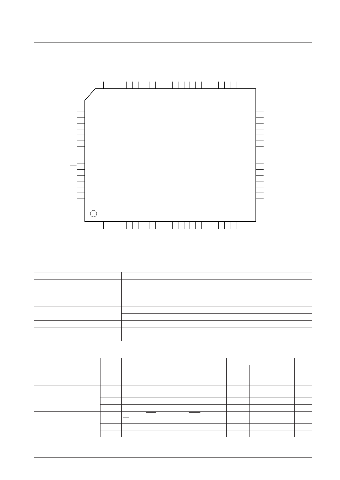
Pin Assignment
No. 6329-3/40
LC78628E
A12796
SQOUT
COIN
CQCK
RES
TST11
SCLK
DQSY
4.2M
LC78628E
SRDT
TEST5
CS
LRSY
CK2
ROMXA
C2F
TEST1
P2
P1
P0
GAIN
DACKO
DFOLO
DFORO
LRCKO
EMPH
TEST4
16M
JP–
JP+
VDD3V
TEST3
HDCD
40
39
38
37
36
35
34
33
32
31
30
29
28
27
26
25
65
66
67
68
69
70
71
72
73
74
75
76
77
78
79
80
RWC64
WRQ63
FSX62
BCKI61
TEST660
DATAI59
EFLG58
LRCKI57
DOUT56
MUTER55
RV
DD
54
RCHP53
RCHN52
RV
SS
51
LV
SS
50
LCHN49
LCHP48
LV
DD
47
MUTEL46
XV
SS
45
XOUT44
XIN43
XV
DD
42
P341
DEFI 1
TAI 2
PDO 3
VV
SS
4
ISET 5
VV
DD
6
FR 7
V
SS
8
V
SS
9
EFMO 10
EFMIN 11
TEST2 12
CLV+ 13
CLV– 14
V/P 15
V
DD
16
P4 17
PCCL 18
HFL 19
TES 20
PCK 21
FSEQ 22
TOFF 23
TGL 24
Parameter Symbol Conditions Ratings Unit
Maximum supply voltage
V
DD
max1 VDD, VVDD, XVDD, LVDD, RV
DD
VSS– 0.3 to VSS+ 6.0 V
V
DD
max2 VDD3V VSS– 0.3 to VSS+ 4.0 V
Input voltage
V
IN
5 max VSS– 0.3 to VDD1 + 0.3 V
V
IN
3 max VSS– 0.3 to VDD2 + 0.3 V
Output voltage
V
OUT
5 max VSS– 0.3 to VDD1 + 0.3 V
V
OUT
3 max VSS– 0.3 to VDD2 + 0.3 V
Allowable power dissipation Pd max 500 mW
Operating temperature Topr –20 to +75 °C
Storage temperature Tstg –40 to +125 °C
Specifications
Absolute Maximum Ratings at Ta = 25°C, VSS= 0 V
Parameter Symbol Conditions
Ratings
Unit
min typ max
Supply voltage
V
DD
1VDD, VVDD, XVDD, LVDD, RV
DD
4.5 5.0 5.5 V
V
DD
2VDD3V 3.0 3.3 3.6 V
V
IH
1
DEFI, COIN, RES, HFL, TES, RWC, CQCK, TAI, SCLK,
0.8 VDD1V
DD
1V
High-level input voltage
CS, PCCL, LRCKI, BCKI, DATAI
V
IH
2 P0 to P4, TEST1 to TEST5, EMPH 0.7 VDD1V
DD
1V
V
IH
3 EFMIN 0.6 VDD1V
DD
1V
V
IL
1
DEFI, COIN, RES, HFL, TES, RWC, CQCK, TAI, SCLK,
0 0.2 VDD1V
Low-level input voltage
CS, PCCL, LRCKI, BCKI, DATAI
V
IL
2 P0 to P4, TEST1 to TEST5, EMPH 0 0.3 VDD1V
V
IL
3 EFMIN 0 0.4 VDD1V
Allowable Operating Conditions at Ta = 25°C, VSS= 0 V
Continued on next page.
No. 6329-4/40
LC78628E
Continued from preceding page.
Notes: The same voltage must be applied to all 5 V system power supply pins.
* When used in conjunction with an ASP that provides a command interface, the stricter ratings of the ASP shall be given priority.
Parameter Symbol Conditions
Ratings
Unit
min typ max
Input level
V
IN
1 EFMIN: Slice level control 1.0 Vp-p
V
IN
2 XIN: Capacitor coupled input 1.0 Vp-p
Data setup time t
SU
COIN, RWC, *: See figure 1. 400 ns
Data hold time t
HD
COIN, RWC, *: See figure 1. 400 ns
High-level clock pulse width t
WH
CQCK, *: See figures 1 and 2. 400 ns
Low-level clock pulse width t
WL
CQCK, *: See figures 1 and 2. 400 ns
Data read access time t
RAC
SQOUT: See figures 2. 0 400 ns
Command output time t
RWC
RWC, *: See figures 1. 1000 ns
Subcode Q readout enable time t
SQE
WRQ, normal speed: See figures 2, RWC = VIL1 11.2 ms
Port input setup time t
CSU
P0 to P4, RWC: See figures 3. 400 ns
Port input hold time t
CHD
P0 to P4, RWC: See figures 3. 400 ns
Port input clock setup time t
RCQ
CQCK, RWC, *: See figures 3. 100 ns
Port output data delay time t
CDD
P0 to P4, RWC: See figure 4. 1200 ns
Text readout period t
CW
DQSY, normal speed: See figure 5. 1.5 3.3 3.7 ms
DQSY pulse width t
W
DQSY, normal speed: See figure 5. 60 136 150 µs
SCLK high-level clock pulse width t
WTH
SCLK: See figure 5. 100 ns
SCLK low-level clock pulse width t
WTL
SCLK: See figure 5. 100 ns
SCLK clock delay time t
D
1 SCLK: See figure 5. 100 ns
Text data delay time
t
D
2 SRDT: See figure 5. 50 ns
t
D
3 SRDT: See figure 5. 50 ns
Reset time t
RES
RES 400 ns
Operating frequency range f
OP
EFMIN 10 MHz
Crystal oscillator frequency f
X
XIN, X
OUT
16.9344 MHz
No. 6329-5/40
LC78628E
Parameter Symbol Conditions
Ratings
Unit
min typ max
Current drain
I
DD
1VDD, VVDD, XVDD, LVDD, RVDD: 4.5 V to 5.5 V 17 24 mA
I
DD
2VDD3V: 3.0 V to 3.6 V 55 85 mA
I
IH
1
DEFI, EFMIN, SCLK, COIN, RES, HFL, TES, RWC, –10 +10 µA
High-level input current
CQCK, TEST1, LRCKI, BCKI, DATAI, XIN: V
IN
= VDD1
I
IH
2 TAI, TEST2 to TEST5, CS, PCCL: VIN= VDD1 10 200 µA
DEFI, EFMIN, SCLK, COIN, RES, HFL, TES, RWC,
Low-level input current I
IL
CQCK, TAI, TEST1 to TEST5, CS, PCCL, LRCKI, BCKI, –10 +10 µA
DATAI, XIN: V
IN
= 0 V
V
OH
1 EFMO: IOH= –1 mA 4 V
CLV
+
, CLV–, V/P, P0 to P4, PCK, FSEQ, TOFF, TGL,
JP
+
, JP–, 16M, EMPH, LRCKO, DACKO, DFOLO,
V
OH
2 DFORO, GAIN, MUTEL, MUTER, DOUT, EFLG, TEST6, VDD1 – 2.1 V
High-level output voltage FSX, WRQ, SQOUT, TST11, DQSY, 4.2M, SRDT, LRSY,
CK2, ROMXA, C2F: I
OH
= –4 mA
V
OH
3 HDCD: IOH= –12 mA VDD1 – 2.1 V
V
OH
4 LCHP, LCHN, RCHP, RCHN: IOH= –1 mA 3.0 4.5 V
V
OL
1 EFMO: IOL= 1 mA 1V
CLV
+
, CLV–, V/P, P0 to P4, PCK, FSEQ, TOFF, TGL,
JP
+
, JP–, 16M, EMPH, LRCKO, DACKO, DFOLO,
Low-level output voltage
V
OL
2 DFORO, GAIN, MUTEL, MUTER, DOUT, EFLG, TEST6, 0.4 V
FSX, WRQ, SQOUT, TST11, DQSY, 4.2M, SRDT, LRSY,
CK2, ROMXA, C2F: I
OL
= 4 mA
V
OL
3 HDCD: IOL= 12 mA 0.4 V
V
OL
4 LCHP, LCHN, RCHP, RCHN: IOH= 1 mA 0.5 2.0 V
Output off leakage current I
OFF
1
PDO, CLV
+
, CLV–, JP+, JP–, P0 to P4, EMPH, SQOUT,
–10 +10 µA
EFMO: In the high-impedance output state
Charge pump output current
I
PDOH
PDO: R
ISET
= 68 kΩ 64 80 96 µA
I
PDOL
PDO: R
ISET
= 68 kΩ –96 –80 –64 µA
Electrical Characteristics at Ta = 25°C, VDD1 = 5 V, VDD2 = 3.3 V, VSS= 0 V

No. 6329-6/40
LC78628E
Parameter Symbol Conditions
Ratings
Unit
min typ max
LCHP, LCHN, RCHP RCHN;
Total harmonic distortion THD + N 1 kHz: 0 dB data input 0.009 0.012 %
With the 20 kHz low-pass filter (internal AD725D) used.
LCHP, LCHN, RCHP, RCHN;
Dynamic range DR
1 kHz: –60 dB data input
83 86 dB
With the 20 kHz low-pass and A filters (internal AD725D)
used.
LCHP, LCHN, RCHP, RCHN;
Signal-to-noise ratio S/N
1 kHz: 0 dB data input
98 103 dB
With the 20 kHz low-pass and A filters (internal AD725D)
used.
LCHP, LCHN, RCHP, RCHN;
Crosstalk (separation) CT 1 kHz: 0 dB data input 96 98 dB
With the 20 kHz low-pass filter (internal AD725D) used.
D/A Converter Block Analog Characteristics at Ta = 25°C, VDD= LVDD= RVDD= XVDD= VVDD= 5 V,
VDD3V = 3.3 V, VSS= LVSS= RVSS= XVSS= VVSS= 0 V.
Figure 1 Command Input
COIN
CQCK
RWC
t
SU
t
SU
t
WL
t
WH
t
HD
t
HD
t
RWC
A12797
Figure 2 Subcode Q Output
t
WH
t
SQE
t
WH
t
WL
WRQ
CQCK
SQOUT
RWC
t
RAC
A12798
Note: Measured in the normal speed playback of the Sanyo 1-bit D/A converter reference circuit.

CQCK
RWC
P0 to P4
HDCD
GAIN
SQOUT
4.2M
RWC
t
CDD
P0 to P4
t
RA
P0 P1 P2 P3 P4
HDCD GAIN
t
CHD
t
RCQ
t
CW
t
CSU
t
D2
t
D3
t
D1
t
WTL
t
W
DQSY
SCLK
SRDT
t
WTL
Flag
D0 D1 D2 D127
A12799
A12800
A12801
No. 6329-7/40
LC78628E
Figure 3 General-Purpose Port Input Timing
Figure 4 General-Purpose Port Output Timing
Figure 5 Text Data Output Timing
Reference Circuit for the 1-Bit D/A Converter Output Block
No. 6329-8/40
LC78628E
+
–
+
–
+
–
+
LC78628E
LV
DD
(RV
DD
)
LV
SS
(RV
SS
)
XOUT
8pF
X'tal:16.9344MHz
8pF
XIN
1MΩ
1kΩ
1kΩ
8.2kΩ
R1
+5V
+10V
–10V
R2
R3
R4
C1
360pF
C6
1200pF
C3
100pF
8.2kΩ
6.2kΩ
24kΩ
R5
C2
C4 R9
R10
47µF
100pF C5 4700pF
6.2kΩ
1.5kΩ
R8
1.5kΩ
10kΩ
100kΩ
LPF
Internal AD725D
manufactured
by Shibasoku.
LCH
(RCH)
Analog output
R11
R13
R12
OP2
OP1
OP3
13kΩ
+10V
10kΩ
+10V
–10V
–10V
R6
24kΩ
R7
10kΩ
LCHP
(RCHP)
LCHN
(RCHN)
A12802
No. 6329-9/40
LC78628E
Pin Functions
Pin No. Pin I/O Function
1 DEFI I Defect detection signal (DEF) input (Must be connected to 0 V if unused.)
2 TAI I Test input. A pull-down resistor is built in. This pin must be connected to 0 V.
3 PDO O External VCO control phase comparator output
4VV
SS
—
PLL-related pins
Internal VCO ground. This pin must be connected to 0 V.
5I
SET
AI PDO output current adjustment resistor connection
6VV
DD
— Internal VCO power supply. 5 V system
7 FR AI VCO frequency range adjustment resistor connection
8V
SS
— Ground. This pin must be connected to 0 V.
9V
SS
— Ground. This pin must be connected to 0 V.
10 EFMO O
Slice level control
EFM signal output
11 EFMIN I EFM signal input
12 TEST2 I Test input. A pull-down resistor is built in. This pin must be connected to 0 V.
13 CLV
+
O
Spindle control servo outputs. CLV
+
outputs a high level for accelerate, and CLV–outputs a high level for decelerate.
14 CLV
–
O
A command is provided to set these pins to three-state output.
15 V/P O
Automatic rough servo/phase control switching monitor output. A high level indicates rough servo and a low level indicates
phase control.
16 V
DD
— 5 V system power supply
17 P4 I/O
General-purpose I/O port. If unused, this port must either be set to input mode and connected to the 0 V level, or be set to
output mode and left open.
General-purpose I/O command identification. A pull-down resistor is built in.
18 PCCL I High: Only general-purpose I/O port commands can be used for control
Low: All commands can be used for control.
19 HFL I Track detection signal input. This is a Schmitt input.
20 TES I Tracking error signal input. This is a Schmitt input.
21 PCK O EFM data reproduction clock monitor output. Outputs 4.3218 MHz when the phase is locked.
Synchronizing signal output.
22 FSEQ O Outputs a high level if the synchronizing signal detected from the EFM signal and the internally generated synchronizing
signal match.
23 TOFF O Tracking off state output
24 TGL O Tracking gain switching output. A low level output raises the gain.
25 HDCD O HDCD identification output. High: An HDCD disc is being played, Low: A normal disc is being played.
26 TEST3 I Test input. A pull-down resistor is built in. This pin must be connected to 0 V.
27 V
DD
3V — 3 V system power supply
28 JP
+
O
Track jump outputs.
JP
+
:
A high level indicates either acceleration during a jump towards outer tracks, or deceleration during a jump towards inner tracks.
29 JP
–
O
JP
–
:
A high level indicates either acceleration during a jump towards inner tracks, or deceleration during a jump towards outer tracks.
A command is provided to set these pins to three-state output.
30 16M O 16.9344 MHz clock output
31 TEST4 I Test input. A pull-down resistor is built in. This pin must be connected to 0 V.
Deemphasis monitor output/input. A high level is output during playback of a deemphasis disc. When external data is applied
32 EMPH I/O to the HDCD filter engine, this pin is used for deemphasis switching. After a reset, this pin goes to monitor output mode in the
high-impedance state.
33 LRCKO O HDCD filter engine output word clock (8fs) or L/R clock output from the HDCD decoder (1fs).
34 DFORO O HDCD filter engine output right channel data (8fs)
35 DFOLO O HDCD filter engine output left channel data (8fs) or L/R data output from the HDCD decoder (1fs).
36 DACKO O HDCD filter engine output bit clock (8fs) or HDCD decoder output bit clock (1fs).
Analog output stage gain indicator
37 GAIN O
In internal gain scaling mode, this pin always outputs a high level (unused). Gain scaling is performed internally. Normal discs
are –6 dB. When external gain scaling is used, peak extend should be turned on when this pin is high, and should be turned
off when this output is low.
38 P0 I/O
General-purpose I/O port. If unused, this port must either be set to input mode and connected to the 0 V level, or be set to
output mode and left open.
39 P1 I/O
General-purpose I/O port. If unused, this port must either be set to input mode and connected to the 0 V level, or be set to
output mode and left open.
40 P2 I/O
General-purpose I/O port. If unused, this port must either be set to input mode and connected to the 0 V level, or be set to
output mode and left open.
41 P3 I/O
General-purpose I/O port. If unused, this port must either be set to input mode and connected to the 0 V level, or be set to
output mode and left open.
Continued on next page.
No. 6329-10/40
LC78628E
Continued from preceding page.
Pin No. Pin I/O Function
42 XV
DD
— Crystal oscillator power supply. 5 V system.
43 X
IN
I
Connections for the 16.9344 crystal element and capacitors. Since no feedback resistor is built in, an external feedback
44 X
OUT
O
resistor must be provided.
45 XV
SS
— Crystal oscillator ground. This pin must be connected to 0 V.
46 MUTEL O Left channel audio data mute detection output
47 LV
DD
— Power supply. 5 V system.
48 LCHP O Left channel audio data P output
49 LCHN O Left channel audio data N output
50 LV
SS
—
Ground. This pin must be connected to 0 V.
51 RV
SS
— Ground. This pin must be connected to 0 V.
52 RCHN O Right channel audio data N output
53 RCHP O Right channel audio data P output
54 RV
DD
— Power supply. 5 V system.
55 MUTER O Right channel audio data mute detection output
56 DOUT O Digital output
57 LRCKI I Left/right clock input for external data input to the HDCD filter engine (1fs)
58 EFLG O C1/C2 single/double error correction monitor output
59 DATAI I Data input for external data input to the HDCD filter engine (20 bits)
60 TEST6 O Test output. Outputs the subcode frame sync signal. This pin must be left open when used.
61 BCKI I Bit clock input for external data input to the HDCD filter engine (48fs)
62 FSX O Outputs the 7.35 kHz sync detection signal divided from the crystal oscillator clock.
63 WRQ O Subcode Q output standby (ready) state output
64 RWC I Read/write control input. This is a Schmitt input.
65 SQOUT O Subcode Q output
66 COIN I Input for commands from the microcontroller
67 CQCK I Command input acquisition clock input, or clock input for readout of subcode data from SQOUT. This is a Schmitt input.
68 RES I IC reset input. Applications must apply a low level to this pin after power is first applied.
69 TST11 O Test output. This pin must be left open (it normally outputs a low level).
70 SCLK I Text data shift clock input
71 DQSY O Text data readout permission output
72 4.2M O 4.2336 MHz output
73 SRDT O Text data output
74 TEST5 I Test input. A pull-down resistor is built in. This pin must be connected to 0 V.
75 CS I Chip select input. A pull-down resistor is built in. (This pin must be connected to 0 V when not controlled.)
76 LRSY O Left/right clock output
77 CK2 O
ROMXA support outputs
Bit clock output (at reset) Polarity inverted clock output (in CK2CON mode)
78 ROMXA O Interpolated data output (at reset) ROM data output (in ROMXA mode)
79 CF2 O C2 flag output
80 TEST1 I Test input. There is no built-in pull-down resistor. This pin must be connected to 0 V.
Note: The equal power-supply voltage must be applied to all the 5 V system power supply pins.
No. 6329-11/40
LC78628E
Internal Functions
1. HF signal input circuit — Pin 11: EFMIN, pin 10: EFMO, pin 1: DEFI, pin 13: CLV
+
When an HF signal is input to the EFMIN pin, an
EFM signal (NRZ) sliced at the optimal level is
acquired. As a measure to handle defects, when the
DEFI pin (pin 1) goes high, the slice level
controller output from the EFMO pin (pin 10) goes
to the high-impedance state, and the slice level is
held. However, this is only valid when the CLV
circuit is in phase control mode, that is, when the
V/P pin (pin 15) is outputting a low level.
This function can be implemented in combination
with the DEF pin from an LA9230/9240 series
product.
*: If the EFMIN and CLV+lines are run close
together, the error rate may increase due to
spurious radiation. We recommend inserting
either a ground or VDDshield line between these
lines.
2. PLL clock regeneration circuit — Pin 3: PDO, pin 5: ISET, pin 7: FR, pin 21: PCK
The LC78628E includes a built-in VCO circuit,
and a PLL circuit is formed by adding external
resistors and capacitors. The ISET pin sets the
charge pump reference current, PDO sets the VCO
circuit loop filter, and FR sets the VCO frequency
range.
Sample values for reference purposes:
R1 = 68 kΩ, C1 = 0.1 µF
R2 = 680 Ω, C2 = 0.1 µF
R3 = 1.2 kΩ
+
–
SLC
SLI
VREF
1110EFMIN
EFMO
HF signal
A12803
V
DD
R1
C2
R2
R3
C1
5 ISET
EFM(NRZ)
PDO
FR
PCK
VCO 1/N
Charge pump
Frequency
and phase
comparator
3
21
7
A12804
Code Command Frequency divisor RES = low
$AC VCO × 2 SET 1
$AD VCO × 1 SET 2
$AE VCO × 0.5 SET 0.5
●●
The divisor used by the divider to create PCK from the VCO can be set using the VCO × 2, VCO ×1, and VCO × 0.5 SET instructions. Normally, the circuit
operates in the VCO × 0.5 SET state after a reset.
3. VCO monitor — Pin 21: PCK
This pin monitors the 4.3218 MHz (on average) signal created by dividing the VCO frequency. In 2 × speed playback
mode, the frequency becomes 8.6436 MHz.
4. Sync detection monitor — Pin 22: FSEQ
When the frame sync (a positive sync signal) read from the EFM signal by PCK and the timing (interpolated sync
signal) generated with a counter match, this pin outputs a high level. Thus this pin functions as a sync detection
monitor. Note that it holds the high level for a single frame.
5. Servo command function — Pin 64: RWC, pin 66: COIN, pin 67: CQCK, pin 18: PCCL
The LC78628E instructions can be executed by setting RWC high and inputting the command to COIN in
synchronization with the CQCK clock. Note that the command is executed starting at the fall of the RWC signal.
Focus start
Track jump
Muting control - - - - - - One-byte commands
Disc motor control
Other control commands
Track check- - - - - - - - - - - - - - - - - - - - - - - - - - - - Two-byte command (RWC set twice)
General-purpose port I/O, E/D settings
Digital attenuator settings - - - - - - Two-byte commands (RWC set once)
HDCD control register settings
No. 6329-12/40
LC78628E
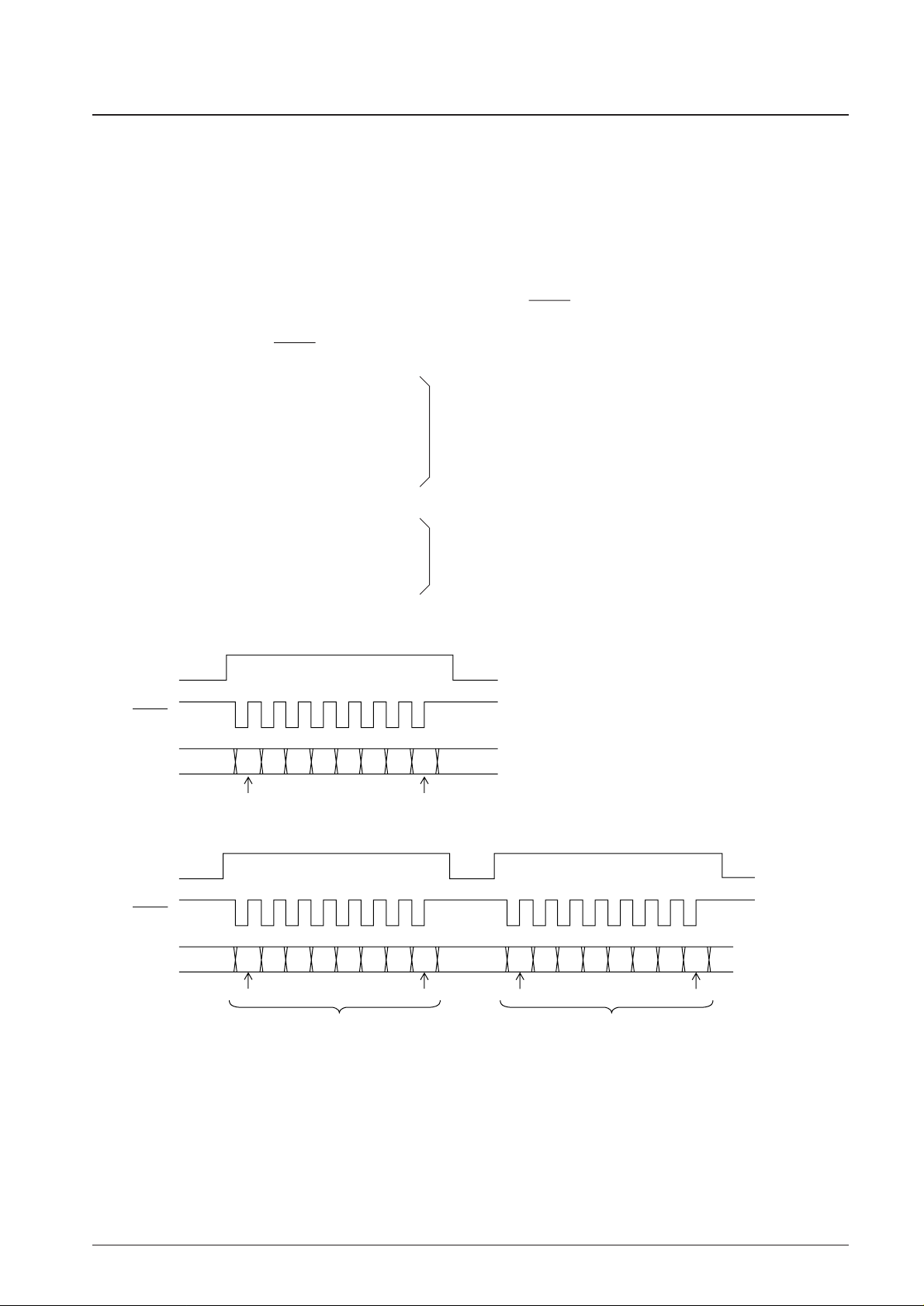
MSBLSB
MSB
LSB
Command ($F0, $F8) Data ($008 to $FE) or command ($FF)
MSB
LSB
RWC
CQCK
COIN
RWC
CQCK
COIN
A12805
A12806
• One-byte commands
• Two-byte command (RWC set twice)
 Loading...