

SANYO LC78212, LC78211 Datasheet

Applications
Function switching under serial data control in amplifiers,
receivers, and other electronic equipment
Features
• Two sets of eight (or in the LC78213, seven) built-in
circuits with three switching configurations available
based on differing internal connections
• Control according to serial data sent from a microprocessor, and easy connection to 5 V microprocessors
• Two identical products can be connected to a shared bus
due to the provision of a select pin (S).
• A reset pin that turns off all analog switches
• A ±20 V withstand voltage rating allows these products
to provide a wide dynamic range.
Package Dimensions
unit: mm
3061-DIP30S
CMOS LSI
Ordering number : EN4817A
73096HA (OT)/72994 TH (OT) No. 4817-1/6
SANYO: DIP30S
[LC78211, 78212, 78213]
SANYO Electric Co.,Ltd. Semiconductor Bussiness Headquarters
TOKYO OFFICE Tokyo Bldg., 1-10, 1 Chome, Ueno, Taito-ku, TOKYO, 110 JAPAN
Analog Function Switch
LC78211, 78212, 78213
Specifications
Absolute Maximum Ratings at Ta = 25°C
Parameter Symbol Conditions Ratings Unit
Maximum supply voltage
V
DD
max V
DD
–0.3 to +20 V
V
EE
max V
EE
–20 to +0.3 V
Maximum input voltage
V
I
1 DI, CL, CE, S, RES –0.3 to +20 V
V
I
2 L1 to L8, R1 to R8, LCOM1 to LCOM4, RCOM1 to RCOM4 VEE– 0.3 to VDD+ 0.3 V
Analog switch potential difference when on ∆V
ON
With the switch on 0.5 V
Allowable power dissipation Pd max Ta ≤ 75°C 100 mW
Operating temperature range Topr –30 to +75 °C
Storage temperature range Tstg –40 to +125 °C
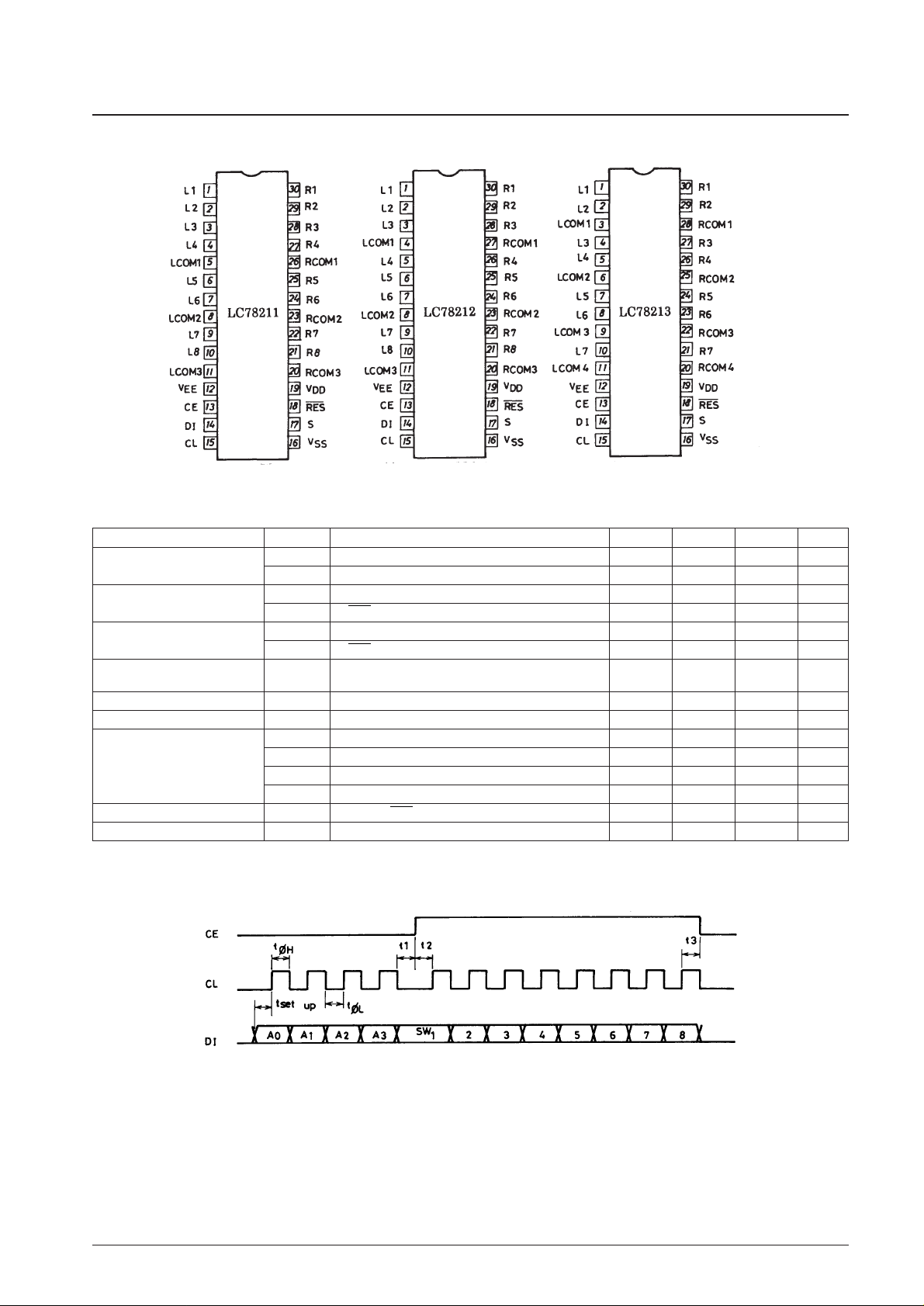
Pin Assignments
Allowable Operating Ranges at Ta = 25°C, VSS= 0 V, | VDD| ≥ | VEE|
Note: * CE, CL and DI waveforms
No. 4817-2/6
LC78211, 78212, 78213
Parameter Symbol Conditions min typ max Unit
Maximum supply voltage
V
DD
VDD– VEE≥ 12 V: V
DD
6.0 18.5 V
V
EE
VDD– VEE≥ 12 V: V
EE
–18.5 0 V
Input high level voltage
V
IH
1 DI, CL, CE 4.0 18.5 V
V
IH
2 S, RES 0.7 V
DD
V
DD
V
Input low level voltage
V
IL
1 DI, CL, CE 0 0.7 V
V
IL
2 S, RES 0 0.3 V
DD
V
Analog switch input
V
IN
L1 to L8, R1 to R8, LCOM1 to LCOM4,
V
EE
V
DD
V
voltage range RCOM1 to RCOM4
Low level clock pulse width t
øL
CL 0.5 µs
High level clock pulse width t
øH
CL 0.5 µs
t
set up
CL, DI 0.5 µs
Setup time
t1* CL, CE 0.5 µs
t2* CL, CE 0.5 µs
t3* CL, CE 0.5 µs
Minimum reset pulse width t
wRESVDD
≥ 6 V: RES 1.0 µs
Hysteresis V
H
CL, CE, DI 0.3 V
Top view
 Loading...