

SANYO LC75878E, LC75878W Datasheet
Ordering number : ENN*6473
41000RM (OT) No. 6473 -1/33
Overview
The LC75878E and LC75878W are 1/8 to 1/10 duty
general-purpose LCD display drivers used for character
and graphics display. These products operate under the
control of a microcontroller and can directly drive an LCD
with up to 730 segments. They can also control up to 4
general-purpose output ports.
Features
• 1/8duty–1/4bias, 1/9duty–1/4bias, and 1/10duty–1/4bias
drive schemes can be controlled from serial data.
1/8duty–1/4bias: up to 600 segments
1/9duty–1/4bias: up to 666 segments
1/10duty–1/4bias: up to 730 segments
• Serial data input supports CCB format communication
with the system controller.
• Serial data control of the power-saving mode based
backup function and all the segments forced off
function.
• Direct display of display data without the use of a
decoder provides high generality.
• Built-in display contrast adjustment circuit.
• Up to 4 general-purpose output ports are included.
• Independent LCD driver block power supply V
LCD
.
• The INH pin is provided. This pin turns off the display
and forces the general-purpose output ports to the low
level.
• RC oscillator circuit
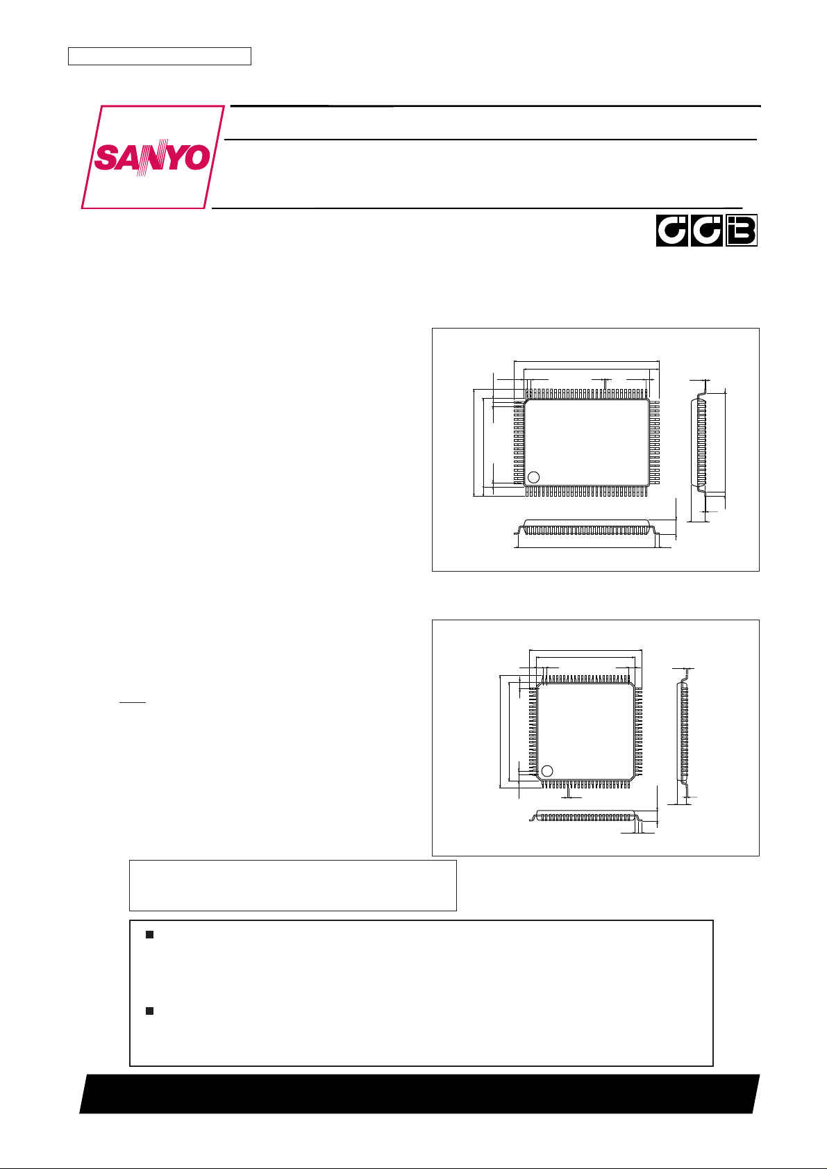
Package Dimensions
unit: mm
3151-QFP100E
unit: mm
3181B-SQFP100
21.6
0.8
3.0max
1.6
17.2
0.825
130
31
50
51
80
81
1.6
0.575
0.575
0.15
2.7
15.6
0.3
20.0
23.2
14.0
0.65
0.825
100
0.8
0.65
0.1
Preliminary
SANYO: QFP100E
[LC75878E]
0.2
1.0
1.0
16.0
14.0
0.5
16.0
14.0
0.5
1.0
1.0
0.145
1.4
1.6max
0.5 0.5
100
125
26
50
5175
76
0.1
SANYO: SQFP100
[LC75878W]
LC75878E, 75878W
SANYO Electric Co.,Ltd. Semiconductor Company
TOKYO OFFICE Tokyo Bldg., 1-10, 1 Chome, Ueno, Taito-ku, TOKYO, 110-8534 JAPAN
1/8 to 1/10 Duty General-Purpose LCD Display Drivers
CMOS IC
Any and all SANYO products described or contained herein do not have specifications that can handle
applications that require extremely high levels of reliability, such as life-support systems, aircraft’s
control systems, or other applications whose failure can be reasonably expected to result in serious
physical and/or material damage. Consult with your SANYO representative nearest you before using
any SANYO products described or contained herein in such applications.
SANYO assumes no responsibility for equipment failures that result from using products at values that
exceed, even momentarily, rated values (such as maximum ratings, operating condition ranges, or other
parameters) listed in products specifications of any and all SANYO products described or contained
herein.
• CCB is a trademark of SANYO ELECTRIC CO., LTD.
• CCB is SANYO’s original bus format and all the bus
addresses are controlled by SANYO.

No. 6473-2/33
LC75878E, 75878W
Pin Assignment
No. 6473-3/33
LC75878E, 75878W
Parameter Symbol Conditions Ratings Unit
Maximum supply voltage
V
DD
max V
DD
–0.3 to +7.0
V
V
LCD
max V
LCD
–0.3 to +12.0
V
IN
1 CE, CL, DI, INH –0.3 to +7.0
Input voltage V
IN
2 OSC –0.3 to VDD+0.3 V
V
IN
3V
LCD
1, V
LCD
2, V
LCD
3, V
LCD
4 –0.3 to V
LCD
+0.3
Output voltage
V
OUT
1 OSC, P1 to P4 –0.3 to VDD+0.3
V
V
OUT
2V
LCD
0, S1 to S75, COM1 to COM10 –0.3 to V
LCD
+0.3
I
OUT
1 S1 to S75 300 µA
Output current I
OUT
2 COM1 to COM10 3
mA
I
OUT
3 P1 to P4 5
Allowable power dissipation Pd max Ta = 85°C 200 mW
Operating temperature Topr –40 to +85 °C
Storage temperature Tstg –55 to +125 °C
Specifications
Absolute Maximum Ratings at Ta=25°C, VSS=0V
Parameter Symbol Conditions
Ratings
Unit
min typ max
V
DDVDD
2.7 6.0
V
LCD
, When the display contrast adjustment 7.0 11.0
Supply voltage
V
LCD
circuit is used V
V
LCD
, When the display contrast adjustment 4.5 11.0
circuit is not used
Output voltage V
LCD
0V
LCD
0
V
LCD
4 + 4.5
V
LCD
V
V
LCD
1V
LCD
1
3/4
V
LCD
0
(V
LCD
0–V
LCD
4)
V
LCD
2V
LCD
2
2/4
V
LCD
0
Input voltage
(V
LCD
0–V
LCD
4)
V
V
LCD
3V
LCD
3
1/4
V
LCD
0
(V
LCD
0–V
LCD
4)
V
LCD
4V
LCD
4 0 1.5
Input high level voltage V
IH
CE, CL, DI, INH 0.8 V
DD
6.0 V
Input low level voltage V
IL
CE, CL, DI, INH 0 0.2 V
DD
V
Recommended external resistance R
OSC
OSC 43 kΩ
Recommended external capacitance C
OSC
OSC 680 pF
Guaranteed oscillation range f
OSC
OSC 25 50 100 kHz
Data setup time t
ds
CL, DI :Figure 2 160 ns
Data hold time t
dh
CL, DI :Figure 2 160 ns
CE wait time t
cp
CE, CL :Figure 2 160 ns
CE setup time t
cs
CE, CL :Figure 2 160 ns
CE hold time t
ch
CE, CL :Figure 2 160 ns
High level clock pulse width tø
H
CL :Figure 2 160 ns
Low level clock pulse width tø
L
CL :Figure 2 160 ns
INH switching time t
c
INH, CE :Figures 3, 4, and 5 10 µs
Allowable Operating Ranges at Ta = –40 to +85°C, VSS=0V
No. 6473-4/33
LC75878E, 75878W
Parameter Symbol Conditions
Ratings
Unit
min typ max
Hysteresis V
H
CE, CL, DI, INH 0.1 V
DD
V
Input high level current I
IH
CE, CL, DI, INH: VI= 6.0 V 5.0 µA
Input low level current I
IL
CE, CL, DI, INH: VI= 0 V –5.0 µA
V
OH
1 S1 to S75: IO= –20 µA
V
LCD
0 – 0.6
Output high level voltage VOH2 COM1 to COM10: IO= –100 µA
V
LCD
0 – 0.6
V
V
OH
3 P1 to P4: IO= –1 mA VDD– 1.0
V
OL
1 S1 to S75: IO= 20 µA
V
LCD
4 + 0.6
Output low level voltage VOL2 COM1 to COM10: IO= 100 µA
V
LCD
4 + 0.6
V
V
OL
3 P1 to P4: IO= 1 mA 1.0
2/4 2/4
V
MID
1 S1 to S75: IO= ±20 µA
(V
LCD
0 – V
LCD
4) (V
LCD
0 – V
LCD
4)
–0.6 +0.6
3/4 3/4
Output middle level voltage * V
MID
2 COM1 to COM10: IO= ±100 µA
(V
LCD
0 – V
LCD
4) (V
LCD
0 – V
LCD
4)
V
–0.6 +0.6
1/4 1/4
V
MID
3 COM1 to COM10: IO= ±100 µA
(V
LCD
0 – V
LCD
4) (V
LCD
0 – V
LCD
4)
–0.6 +0.6
Oscillator frequency fosc OSC: R
OSC
= 43 kΩ, C
OSC
= 680 pF 40 50 60 kHz
I
DD
1VDD: Power saving mode 5
I
DD
2VDD: VDD= 6.0 V,
outputs open, fosc = 50 kHz
200 400
I
LCD
1V
LCD
: Power saving mode 5
V
LCD
: V
LCD
= 11.0 V
I
LCD
2
Outputs open
500 1000 µA
Current drain
fosc = 50 kHz
When the display contrast adjustment circuit is used.
V
LCD
: V
LCD
= 11.0 V
I
LCD
3
Outputs open
250 500
fosc = 50 kHz
When the display contrast adjustment circuit is not used.
Electrical Characteristics for the Allowable Operating Ranges
Note: * Excluding the bias voltage generation divider resistor built into V
LCD
0, V
LCD
1, V
LCD
2 , V
LCD
3, and V
LCD
4. (See Figure 1.)

No. 6473-5/33
LC75878E, 75878W
Figure 1
• When CL is stopped at the low level
Figure 2
• When CL is stopped at the high level
To the common and segment drivers
Excluding these resistors
CONTRAST
ADJUSTER
No. 6473-6/33
LC75878E, 75878W
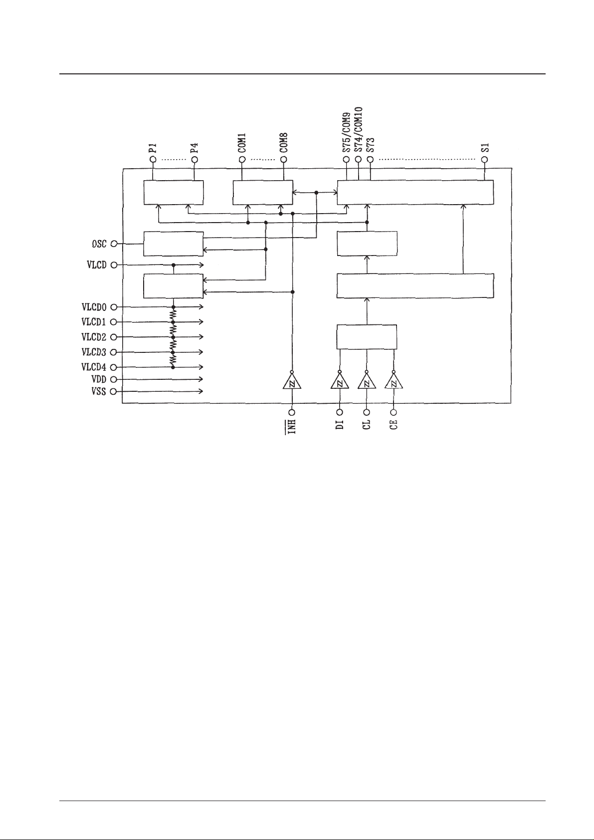
Block Diagram
GENERAL PORT
COMMON
DRIVER
SEGMENT DRIVER & LATCH
CONTROL
REGISTER
CLOCK
GENERATOR
CONTRAST
ADJUSTER
SHIFT REGISTER
CCB INTERFACE

No. 6473 -7/39
LC75878E, 75878W
Pin
Pin No.
Function Active I/O
Handling
LC75878E LC75878W
when unused
S1 to S73 3 to 75 1 to 73 Segment driver outputs.
S74/COM10 76 74 The S74/COM10 and S75/COM9 pins can be used as common — ●● Open
S75/COM9 77 75 driver outputs under the control data.
COM1 to COM8
85 to 78 83 to 76 Common driver outputs. — ●● Open
P1 to P4 86 to 89 84 to 87 General-purpose output ports. — ●● Open
OSC 98 96 — I/O V
DD
CE 100 98 HI
CL 1 99 I GND
DI 2 100 —I
INH 99 97 L I GND
V
LCD
092 90 — O Open
V
LCD
193 91 — I Open
V
LCD
294 92 — I Open
V
LCD
395 93 — I Open
V
LCD
496 94 — I GND
V
DD
90 88 —— —
V
LCD
91 89 —— —
V
SS
97 95 Power supply connection. Connect to ground. — — —
Pin Functions
Oscillator connection.
An oscillator circuit is formed by connecting an external resistor and
capacitor at this pin.
Serial data transfer inputs.
These pins are connected to the microcontroller.
CE :Chip enable
CL :Synchronization clock
DI :Transfer data
▲
Input that turns the display off and forces the general-purpose output
ports low.
• When INH is low (V
SS
)
• Display off
S1 to S73 = “L” (V
LCD
4).
S74/COM10, S75/COM9 = “L” (V
LCD
4)
COM1 to COM8 = “L” (V
LCD
4).
• General-purpose output ports P1 to P4 = low (V
SS
)
• When INH is high (V
DD
)
• Display on
• The states of the general-purpose output ports can be set by
the PC1 to PC4 control data.
However, serial data can be transferred when the INH pin is low.
LCD drive 3/4 bias voltage (middle level) supply pin. This pin can be
used to supply the 3/4 (V
LCD
0 – V
LCD
4) voltage level externally.
LCD drive 2/4 bias voltage (middle level) supply pin. This pin can be
used to supply the 2/4 (V
LCD
0 – V
LCD
4) voltage level externally.
LCD drive 1/4 bias voltage (middle level) supply pin. This pin can be
used to supply the 1/4 (V
LCD
0 – V
LCD
4) voltage level externally.
LCD drive 0/4 bias voltage (low level) supply pin. Fine adjustment of the
display contrast can be implemented by connecting an external variable
resistor to this pin.
However, (V
LCD
0 – V
LCD
4) must be greater than or equal to 4.5 V, and
V
LCD
4 must be in the range 0 V to 1.5 V, inclusive.
Logic block power supply connection. Provide a voltage of between 2.7
and 6.0V.
LCD driver block power supply connection. Provide a voltage of between
7.0 and 11.0 V when the display contrast adjustment circuit is used and
provide a voltage of between 4.5 and 11.0 V when the circuit is not used.
LCD drive 4/4 bias voltage (high level) supply pin. The level on this pin
can be changed by the display contrast adjustment circuit.
However, (V
LCD
0 – V
LCD
4) must be greater than or equal to 4.5 V.
Also,external power must not be applied to this pin since the pin circuit
includes the display contrast adjustment circuit.
No. 6473-8/33
LC75878E, 75878W
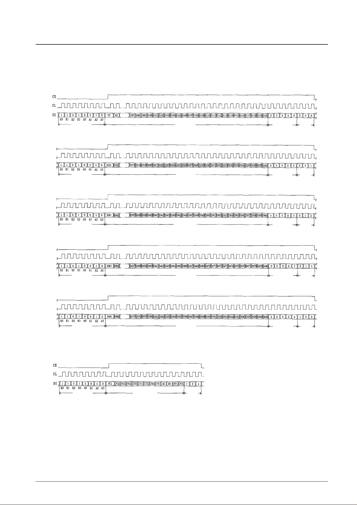
Serial Data Transfer Format
1. 1/8 duty
① When CL is stopped at the low level
• When the display data is transferred.
• When the control data is transferred.
Note: B0 to B3, A0 to A3
......
CCB address
DD
................................
Direction data
Display
data
120 bits
Fixed
data
5 bits
DD
3 bits
CCB
address
8 bits
CCB
address
8 bits
CCB
address
8 bits
Display
data
120 bits
Fixed
data
5 bits
Fixed
data
5 bits
Display
data
120 bits
DD
3 bits
DD
3 bits
CCB
address
8 bits
CCB
address
8 bits
Display
data
120 bits
Display
data
120 bits
Fixed
data
5 bits
Fixed
data
5 bits
DD
3 bits
DD
3 bits
CCB
address
8 bits
Control
data
13 bits
DD
3 bits
No. 6473-9/33
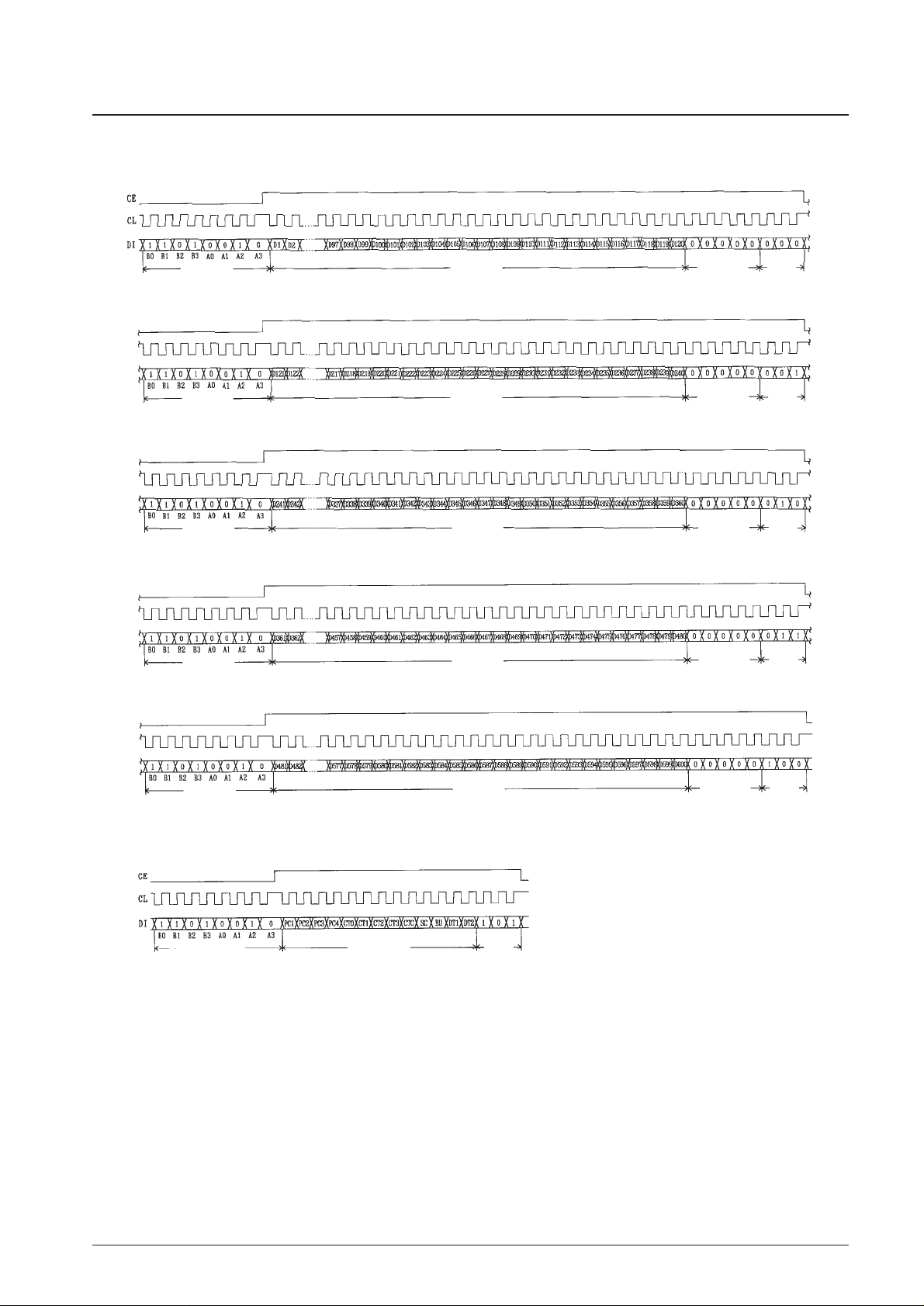
LC75878E, 75878W
② When CL is stopped at the high level
• When the display data is transferred.
Note: B0 to B3, A0 to A3
......
CCB address
DD
................................
Direction data
• CCB address: ....4BH
• D1 to D600: ........ Display data
• PC1 to PC4: ........ General-purpose output port state setting data
• CT0 to CT3, CTC: Display contrast setting data
• SC: ...................... Segment on/off control data
• BU: ...................... Normal mode/power saving mode control data
• DT1, DT2:............ Display technique setting data
• When the control data is transferred.
CCB
address
8 bits
Display
data
120 bits
Fixed
data
5 bits
DD
3 bits
Control
data
13 bits
CCB
address
8 bits
CCB
address
8 bits
CCB
address
8 bits
CCB
address
8 bits
Display
data
120 bits
Display
data
120 bits
Display
data
120 bits
Display
data
120 bits
Fixed
data
5 bits
Fixed
data
5 bits
Fixed
data
5 bits
Fixed
data
5 bits
DD
3 bits
DD
3 bits
DD
3 bits
DD
3 bits
CCB
address
8 bits
DD
3 bits
No. 6473-10/33
LC75878E, 75878W
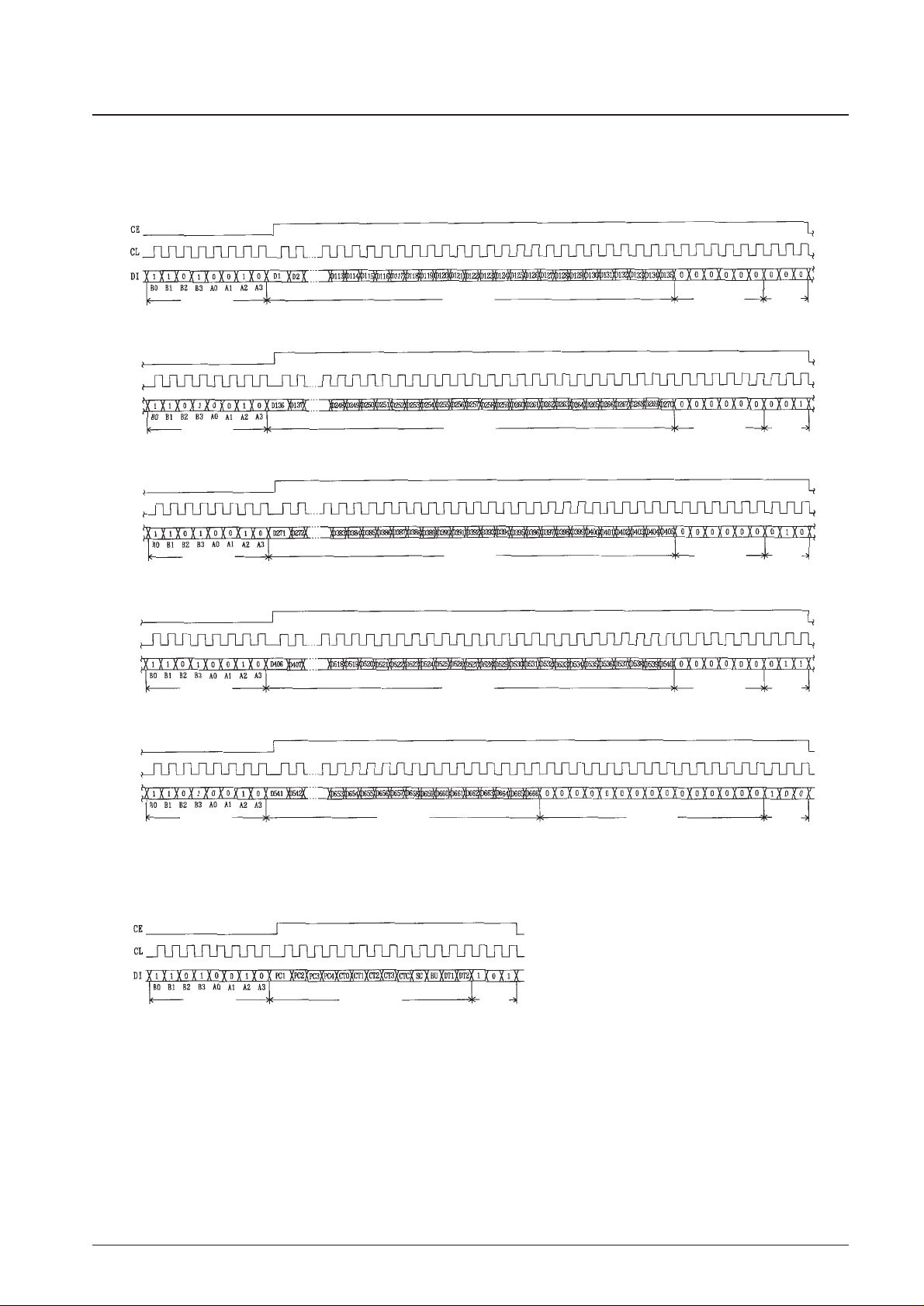
2. 1/9 duty
① When CL is stopped at the low level
• When the display data is transferred.
• When the control data is transferred.
Note: B0 to B3, A0 to A3
......
CCB address
DD
................................
Direction data
Control
data
13 bits
CCB
address
8 bits
Display
data
135 bits
Fixed
data
6 bits
DD
3 bits
CCB
address
8 bits
CCB
address
8 bits
CCB
address
8 bits
CCB
address
8 bits
Display
data
135 bits
Display
data
135 bits
Display
data
135 bits
Display
data
126 bits
Fixed
data
6 bits
Fixed
data
6 bits
Fixed
data
6 bits
Fixed
data
15 bits
DD
3 bits
DD
3 bits
DD
3 bits
DD
3 bits
DD
3 bits
CCB
address
8 bits
 Loading...