

SANYO LC75874W, LC75874E Datasheet

Overview
The LC75874E and LC75874W are 1/4-duty generalpurpose microprocessor-controlled LCD driver that can be
used in applications such as frequency display in products
with electronic tuning. In addition to being able to drive
up to 264 segments directly, the LC75874E and
LC75874W can also control up to 8 general-purpose
output ports.
Since the LC75874E and LC75874W use separate power
supply systems for the LCD drive block and the logic
block, the LCD driver block power-supply voltage can be
set to any voltage in the range 2.7 to 6.0 V, regardless of
the logic block power-supply voltage.
Features
• Support for 1/4-duty 1/2-bias or 1/4-duty 1/3-bias drive
techniques under serial data control (up to
264 segments)
• Serial data input supports CCB format communication
with the system controller.
• Serial data control of the power-saving mode based
backup function and the all segments forced off
function.
• Serial data control of switching between the segment
output port and general-purpose output port functions.
• High generality, since display data is displayed directly
without the intervention of a decoder circuit.
• Independent V
LCD
for the LCD driver block (V
LCD
can
be set to any voltage in the range 2.7 to 6.0 V,
regardless of the logic block power-supply voltage.)
• The INH pin allows the display to be forced to the off
state.
• RC oscillator circuit
Package Dimensions
unit: mm
3174-QFP80E
unit: mm
3220-SQFP80
CMOS LSI
Ordering number : EN5800
31398RM (OT) No. 5800-1/16
SANYO Electric Co.,Ltd. Semiconductor Bussiness Headquarters
TOKYO OFFICE Tokyo Bldg., 1-10, 1 Chome, Ueno, Taito-ku, TOKYO, 110-8534 JAPAN
LC75874E, 75874W
1/4-Duty General-Purpose LCD Display Driver
[LC75874E]
SANYO: QFP80E
[LC75874W]
SANYO: SQFP80
• CCB is a trademark of SANYO ELECTRIC CO., LTD.
• CCB is SANYO’s original bus format and all the bus
addresses are controlled by SANYO.
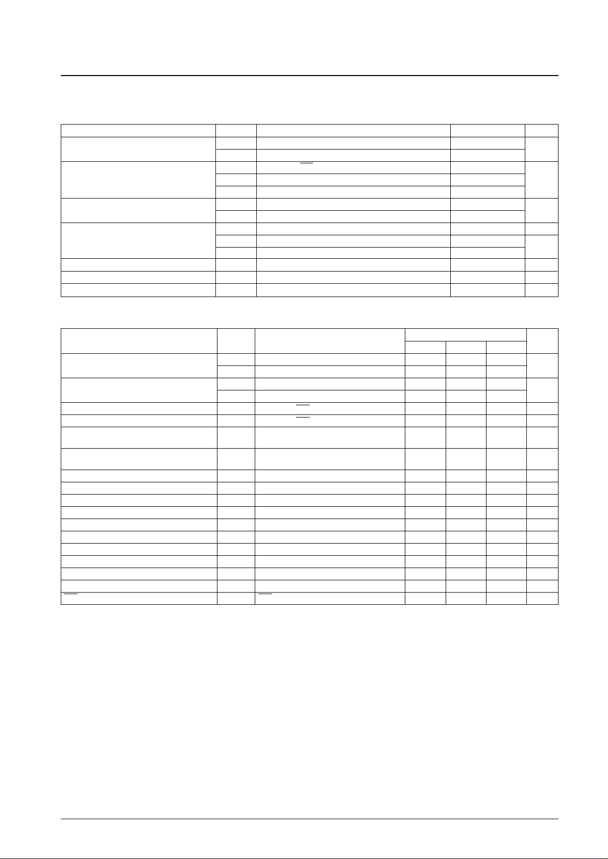
Specifications
Absolute Maximum Ratings at Ta = 25°C, VSS= 0 V
No. 4465-No. 5800-2/16
LC75874E, 75874W
Parameter Symbol Conditions Ratings Unit
Maximum supply voltage
V
DD
max V
DD
–0.3 to +7.0
V
V
LCD
max V
LCD
–0.3 to +7.0
V
IN
1 CE, CL, DI, INH –0.3 to +7.0
Input voltage V
IN
2 OSC –0.3 to VDD+ 0.3 V
V
IN
3 V
LCD
1, V
LCD
2 –0.3 to V
LCD
+ 0.3
Output voltage
V
OUT
1 OSC –0.3 to V
DD
+ 0.3
V
V
OUT
2 S1 to S66, COM1 to COM4, P1 to P8 –0.3 to V
LCD
+ 0.3
I
OUT
1 S1 to S66 300 µA
Output current I
OUT
2 COM1 to COM4 3
mA
I
OUT
3 P1 to P8 5
Allowable power dissipation Pd max Ta = 85°C 200 mW
Operating temperature Topr –40 to +85 °C
Storage temperature Tstg –55 to +125 °C
Parameter Symbol Conditions
Ratings
Unit
min typ max
Supply voltage
V
DD
V
DD
2.7 6.0
V
V
LCDVLCD
2.7 6.0
Input voltage
V
LCD
1 V
LCD
1 2/3 V
LCD
V
LCD
V
V
LCD
2 V
LCD
2 1/3 V
LCD
V
LCD
Input high-level voltage V
IH
CE, CL, DI, INH 0.8 V
DD
6.0 V
Input low-level voltage V
IL
CE, CL, DI, INH 0 0.2 V
DD
V
Recommended external
R
OSC
OSC 43 kΩ
resistance
Recommended external
C
OSC
OSC 680 pF
capacitance
Guaranteed oscillation range f
OSC
OSC 25 50 100 kHz
Data setup time t
ds
CL, DI: Figure 2 160 ns
Data hold time t
dh
CL, DI: Figure 2 160 ns
CE wait time t
cp
CE, CL: Figure 2 160 ns
CE setup time t
cs
CE, CL: Figure 2 160 ns
CE hold time t
ch
CE, CL: Figure 2 160 ns
High-level clock pulse width t
øH
CL: Figure 2 160 ns
Low-level clock pulse width t
øL
CL: Figure 2 160 ns
Rise time t
r
CE, CL, DI: Figure 2 160 ns
Fall time t
f
CE, CL, DI: Figure 2 160 ns
INH switching time t
c
INH, CE: Figure 3 10 µs
Allowable Operating Ranges at Ta = –40 to +85°C, VSS= 0 V

Note: *1 Excluding the bias voltage generation divider resistors built in the V
LCD
1 and V
LCD
2. (See Figure 1.)
No. 4465No. 5800-3/16
LC75874E, 75874W
Parameter Symbol Conditions
Ratings
Unit
min typ max
Hysteresis V
H
CE, CL, DI, INH 0.1 V
DD
V
Input high-level current I
IH
CE, CL, DI, INH: VI= 6.0 V 5.0 µA
Input low-level current I
IL
CE, CL, DI, INH: VI= 0 V –5.0 µA
V
OH
1 S1 to S66: IO= –20 µA V
LCD
– 0.9
Output high-level voltage V
OH
2 COM1 to COM4: IO= –100 µA V
LCD
– 0.9 V
V
OH
3 P1 to P8: IO= –1 mA V
LCD
– 0.9
V
OL
1 S1 to S66: IO= 20 µA 0.9
Output low-level voltage V
OL
2 COM1 to COM4: IO= 100 µA 0.9 V
V
OL
3 P1 to P8: IO= 1 mA 0.9
V
MID
1 COM1 to COM4: 1/2 bias, IO= ±100 µA
1/2 V
LCD
– 1/2 V
LCD
+
0.9 0.9
V
MID
2 S1 to S66: 1/3 bias, IO= ±20 µA
2/3 V
LCD
– 2/3 V
LCD
+
0.9 0.9
Output middle-level voltage*1 V
MID
3 S1 to S66: 1/3 bias, IO= ±20 µA
1/3 V
LCD
– 1/3 V
LCD
+
V
0.9 0.9
V
MID
4 COM1 to COM4: 1/3 bias, IO= ±100 µA
2/3 V
LCD
– 2/3 V
LCD
+
0.9 0.9
V
MID
5 COM1 to COM4: 1/3 bias, IO= ±100 µA
1/3 V
LCD
– 1/3 V
LCD
+
0.9 0.9
Oscillator frequency f
OSC
OSC: R
OSC
= 43 kΩ, C
OSC
= 680 pF 40 50 60 kHz
I
DD
1 V
DD
: Power-saving mode 5
I
DD
2 VDD: VDD= 6.0 V, outputs open, f
OSC
= 50 kHz 230 460
Current drain I
LCD
1 V
LCD
: Power-saving mode 5 µA
I
LCD
2 V
LCD
:
V
LCD
= 6.0 V, outputs open, 1/2 bias, f
OSC
= 50 kHz
200 400
I
LCD
3 V
LCD
:
V
LCD
= 6.0 V, outputs open, 1/3 bias, f
OSC
= 50 kHz
120 240
Electrical Characteristics for the Allowable Operating Ranges
Figure 1
V
LCD
V
LCD
1
V
LCD
2

1. When CL is stopped at the low level
2. When CL is stopped at the high level
Figure 2
Block Diagram
No. 4465-No. 5800-4/16
LC75874E, 75874W
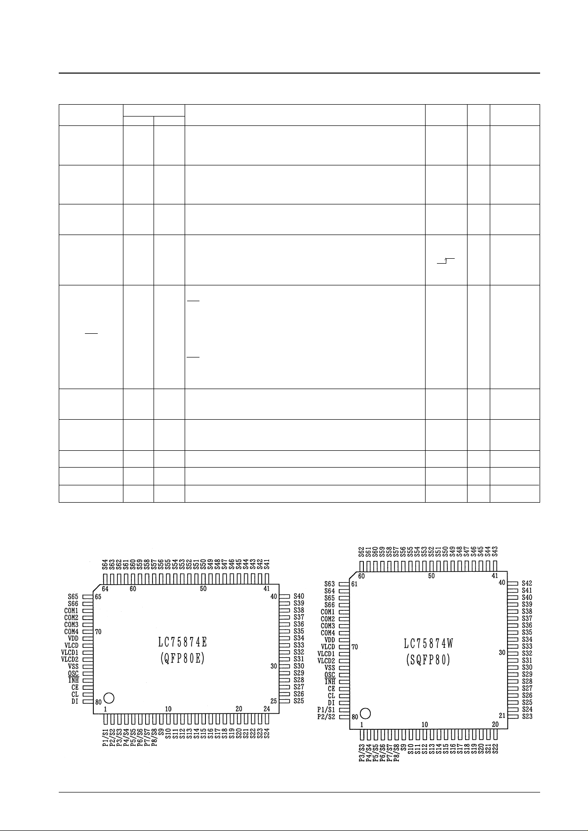
Pin Functions
No. 4465No. 5800-5/16
LC75874E, 75874W
Symbol
Pin No.
Function Active I/O
Handling
LC75874ELC75874W
when unused
1 to 8
9 to 66
79, 80,
1 to 6
7 to 64
67
68
69
70
65
66
67
68
76
74
78
76
79
80
78
77
77
75
73
71
74
72
71
69
72
70
S1/P1 to S8/P8
S9 to S66
COM1
COM2
COM3
COM4
OSC
CE
CL
DI
INH
V
LCD
1
V
LCD
2
V
DD
V
LCD
Segments outputs for displaying the display data transferred by serial data
input. The S1/P1 to S8/P8 pins can be used as general-purpose output
ports under serial data control.
Common driver outputs. The frame frequency fo is f
OSC
/512 Hz.
Oscillator connection. An oscillator circuit can be formed by connecting an
external resistor and capacitor at this pin.
Serial data transfer inputs. Connected to the controller.
CE: Chip enable
CL: Synchronization clock
DI: Transfer data
Display off control input
INH = low (V
SS
)......Display forced off
S1/P1 to S8/P8 = low (V
SS
)
(These pins are forcibly set to the segment output port
function and held at the V
SS
level.)
S9 to S66 = low (V
SS
)
COM1 to COM4 = low (V
SS
)
INH = high (V
DD
).....Display on
However, serial data transfer is possible when the display is forced off by
this pin.
Used to apply the LCD drive 2/3 bias voltage externally. Connect this pin to
V
LCD
2 when using a 1/2-bias drive scheme.
Used to apply the LCD drive 1/3 bias voltage externally. Connect this pin to
V
LCD
1 when using a 1/2-bias drive scheme.
Logic block power supply. In the range 2.7 to 6.0 V.
LCD driver block power supply. In the range 2.7 to 6.0 V.
—
—
—
H
—
L
—
—
—
—
O
O
I/O
I
I
I
I
I
I
—
—
Open
Open
V
DD
GND
GND
Open
Open
—
—
75
73
V
SS
Ground pin. Connect to ground. — — —
Pin Assignments
Top view
 Loading...