

Sanyo LC75848T Specifications
Ordering number : ENN7160
42202AS (OT) No. 7160 -1/33
Overview
The LC75848T is 1/8 to 1/10 duty general-purpose LCD
display drivers used for character and graphics display.
These products operate under the control of a
microcontroller and can directly drive an LCD with up to
930 segments. They can also control up to 4 generalpurpose output ports.
Features
• 1/8duty–1/4bias, 1/9duty–1/4bias, and 1/10duty–1/4bias
drive schemes can be controlled from serial data.
1/8duty–1/4bias: up to 760 segments
1/9duty–1/4bias: up to 846 segments
1/10duty–1/4bias: up to 930 segments
• Serial data input supports CCB format communication
with the system controller.
• Serial data control of the power-saving mode based
backup function and all the segments forced off
function.
• The frame frequency of the common and segment output
waveforms can be controlled from the serial data.
• Direct display of display data without the use of a
decoder provides high generality.
• Built-in display contrast adjustment circuit.
• Up to 4 general-purpose output ports are included.
• Independent LCD driver block power supply V
LCD
.
• The INH pin is provided. This pin turns off the display
and forces the general-purpose output ports to the low
level.
• RC oscillator circuit
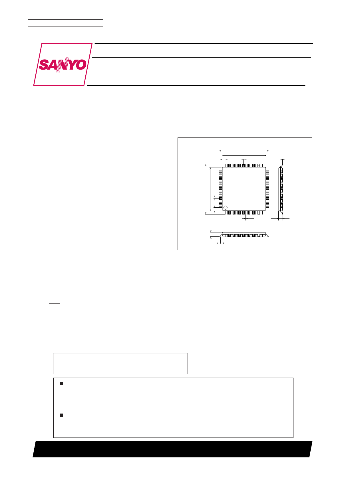
Package Dimensions
unit: mm
3257-TQFP120
120
130
31
60
6190
91
0.4
14.0
(1.2)
(0.5)
0.125
16.0
0.5
0.15
1.2max
0.1
0.4
14.0
(1.2)
(1.0)
16.0
SANYO: TQFP120
[LC75848T]
LC75848T
SANYO Electric Co.,Ltd. Semiconductor Company
TOKYO OFFICE Tokyo Bldg., 1-10, 1 Chome, Ueno, Taito-ku, TOKYO, 110-8534 JAPAN
1/8 to 1/10 Duty General-Purpose LCD Display Drivers
CMOS IC
Any and all SANYO products described or contained herein do not have specifications that can handle
applications that require extremely high levels of reliability, such as life-support systems, aircraft’s
control systems, or other applications whose failure can be reasonably expected to result in serious
physical and/or material damage. Consult with your SANYO representative nearest you before using
any SANYO products described or contained herein in such applications.
SANYO assumes no responsibility for equipment failures that result from using products at values that
exceed, even momentarily, rated values (such as maximum ratings, operating condition ranges, or other
parameters) listed in products specifications of any and all SANYO products described or contained
herein.
• CCB is a trademark of SANYO ELECTRIC CO., LTD.
• CCB is SANYO’s original bus format and all the bus
addresses are controlled by SANYO.
No. 7160-2/33
LC75848T
Pin Assignment
COM8
VDD
VLCD1
VLCD0
S75
S81
S82
S83
S74
S76
S77
S78
S79
S80
S61
S62
S63
S64
S65
S66
S67
S68
S69
S70
S71
S72
S73
S5
S11
S4
S3
S2
S1
COM7
COM5
COM6
COM4
LC75848T
(TQFP120)
COM3
COM2
COM1
P2
P1
P4
P3
VLCD
VLCD2
VLCD3
VSS
VLCD4
OSC
CE
INH
CL
S40
S39
S38
S37
S36
S34
S35
S32
S33
S31DI
61
90
6091
31120
301
S10
S9
S8
S7
S6
S16
S22
S15
S14
S13
S12
S21
S20
S19
S18
S17
S25
S24
S23
S45
S44
S43
S42
S41
S50
S49
S48
S47
S46
S55
S54
S53
S52
S51
S26
S27
S29
S30
S28
S60
S59
S58
S57
S56
S85
S84
S86
S87
S88
S89
S90
S91
S92
S93
COM10/S94
COM9/S95
Top view
No. 7160-3/33
LC75848T
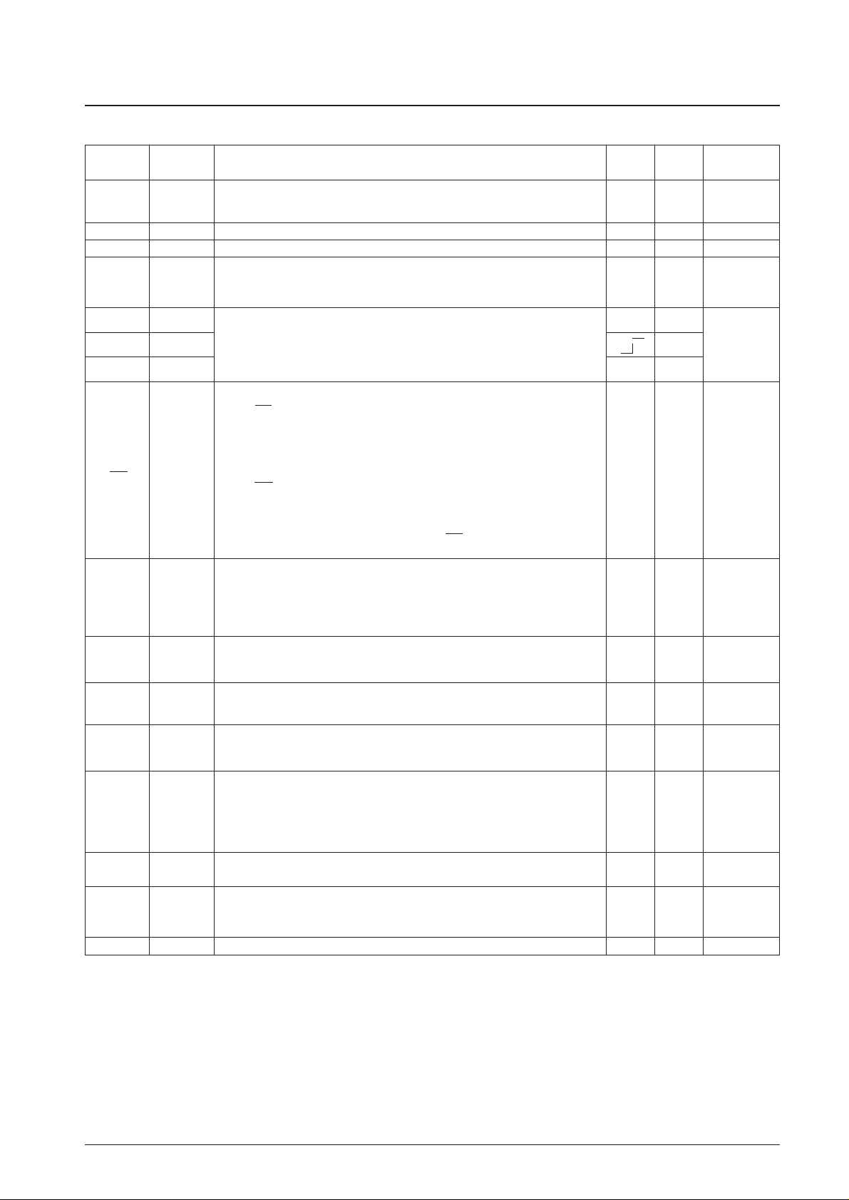
Parameter Symbol Conditions Ratings Unit
Maximum supply voltage
V
DD
max V
DD
–0.3 to +7.0
V
V
LCD
max V
LCD
–0.3 to +12.0
V
IN
1 CE, CL, DI, INH –0.3 to +7.0
Input voltage V
IN
2 OSC –0.3 to VDD+0.3 V
V
IN
3 V
LCD
1, V
LCD
2, V
LCD
3, V
LCD
4 –0.3 to V
LCD
+0.3
Output voltage
V
OUT
1 OSC, P1 to P4 –0.3 to VDD+0.3
V
V
OUT
2 V
LCD
0, S1 to S95, COM1 to COM10 –0.3 to V
LCD
+0.3
I
OUT
1 S1 to S95 300 µA
Output current I
OUT
2 COM1 to COM10 3
mA
I
OUT
3 P1 to P4 5
Allowable power dissipation Pd max Ta = 85°C 200 mW
Operating temperature Topr –40 to +85 °C
Storage temperature Tstg –55 to +125 °C
Specifications
Absolute Maximum Ratings at Ta=25°C, VSS=0V
Parameter Symbol Conditions
Ratings
Unit
min typ max
V
DDVDD
2.7 6.0
V
LCD
, When the display contrast adjustment 7.0 11.0
Supply voltage
V
LCD
circuit is used V
V
LCD
, When the display contrast adjustment 4.5 11.0
circuit is not used
Output voltage V
LCD
0 V
LCD
0
V
LCD
4 + 4.5
V
LCD
V
V
LCD
1 V
LCD
1
3/4
V
LCD
0
(V
LCD
0–V
LCD
4)
V
LCD
2 V
LCD
2
2/4
V
LCD
0
Input voltage
(V
LCD
0–V
LCD
4)
V
V
LCD
3 V
LCD
3
1/4
V
LCD
0
(V
LCD
0–V
LCD
4)
V
LCD
4 V
LCD
4 0 1.5
Input high level voltage V
IH
CE, CL, DI, INH 0.8 V
DD
6.0 V
Input low level voltage V
IL
CE, CL, DI, INH 0 0.2 V
DD
V
Recommended external resistance R
OSC
OSC 43 kΩ
Recommended external capacitance C
OSC
OSC 680 pF
Guaranteed oscillation range f
OSC
OSC 25 50 100 kHz
Data setup time t
ds
CL, DI :Figure 2 160 ns
Data hold time t
dh
CL, DI :Figure 2 160 ns
CE wait time t
cp
CE, CL :Figure 2 160 ns
CE setup time t
cs
CE, CL :Figure 2 160 ns
CE hold time t
ch
CE, CL :Figure 2 160 ns
High level clock pulse width tø
H
CL :Figure 2 160 ns
Low level clock pulse width tø
L
CL :Figure 2 160 ns
INH switching time t
c
INH, CE :Figures 3, 4, and 5 10 µs
Allowable Operating Ranges at Ta = –40 to +85°C, VSS=0V
No. 7160-4/33
LC75848T
Parameter Symbol Conditions
Ratings
Unit
min typ max
Hysteresis V
H
CE, CL, DI, INH 0.1 V
DD
V
Input high level current I
IH
CE, CL, DI, INH: VI= 6.0 V 5.0 µA
Input low level current I
IL
CE, CL, DI, INH: VI= 0 V –5.0 µA
V
OH
1 S1 to S95: IO= –20 µA
V
LCD
0 – 0.6
Output high level voltage VOH2 COM1 to COM10: IO= –100 µA
V
LCD
0 – 0.6
V
V
OH
3 P1 to P4: IO= –1 mA VDD– 1.0
V
OL
1 S1 to S95: IO= 20 µA
V
LCD
4 + 0.6
Output low level voltage VOL2 COM1 to COM10: IO= 100 µA
V
LCD
4 + 0.6
V
V
OL
3 P1 to P4: IO= 1 mA 1.0
2/4 2/4
V
MID
1 S1 to S95: IO= ±20 µA
(V
LCD
0 – V
LCD
4) (V
LCD
0 – V
LCD
4)
–0.6 +0.6
3/4 3/4
Output middle level voltage *
1
V
MID
2 COM1 to COM10: IO= ±100 µA
(V
LCD
0 – V
LCD
4) (V
LCD
0 – V
LCD
4)
V
–0.6 +0.6
1/4 1/4
V
MID
3 COM1 to COM10: IO= ±100 µA
(V
LCD
0 – V
LCD
4) (V
LCD
0 – V
LCD
4)
–0.6 +0.6
Oscillator frequency fosc OSC: R
OSC
= 43 kΩ, C
OSC
= 680 pF 40 50 60 kHz
I
DD
1 VDD: Power saving mode 5
I
DD
2 VDD: VDD= 6.0 V,
outputs open, fosc = 50 kHz
200 400
I
LCD
1 V
LCD
: Power saving mode 5
V
LCD
: V
LCD
= 11.0 V
I
LCD
2
Outputs open
500 1000 µA
Current drain
fosc = 50 kHz
When the display contrast adjustment circuit is used.
V
LCD
: V
LCD
= 11.0 V
I
LCD
3
Outputs open
250 500
fosc = 50 kHz
When the display contrast adjustment circuit is not used.
Electrical Characteristics for the Allowable Operating Ranges
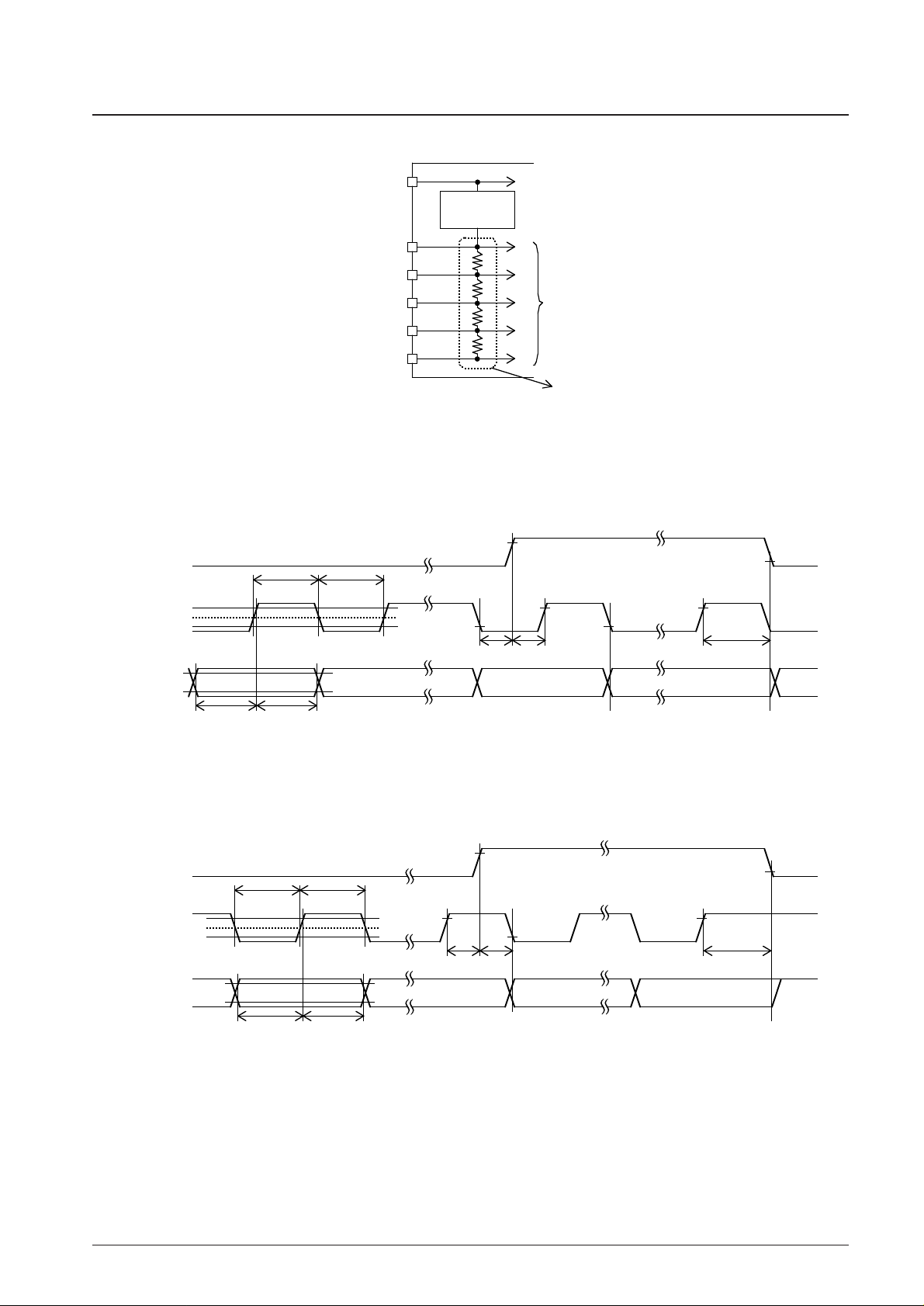
Note: *1. Excluding the bias voltage generation divider resistor built into V
LCD
0, V
LCD
1, V
LCD
2 , V
LCD
3, and V
LCD
4. (See Figure 1.)
No. 7160-5/33
LC75848T
Figure 1
• When CL is stopped at the low level
Figure 2
Excluding these resistors
To the common and segment drivers
VLCD
VLCD3
VLCD4
VLCD2
VLCD0
VLCD1
CONTRAST
ADJUSTER
tds
VIL
VIL
VIL
VIH
50%
VIH
VIH
tchtcs
tcp
tdh
tøLtøH
CE
CL
DI
tds
VIL
VIL
VIL
VIH
VIH
50%
VIH
tchtcstcp
tdh
tøHtøL
CE
CL
DI
• When CL is stopped at the high level
No. 7160-6/33
LC75848T
Block Diagram
S94/COM10
S95/COM9
CE
CL
DI
S1
S93
COM8
COM1
P4
P1
VDD
VLCD3
VLCD4
VLCD1
VLCD2
VLCD0
VLCD
OSC
CONTROL
REGISTER
SEGMENT DRIVER & LATCH
CCB
INTERFACE
COMMON
DRIVER
GENERAL
PORT
CLOCK
GENERATOR
CONTRAST
ADJUSTER
VSS
INH
SHIFT REGISTER
No. 7160-7/33
LC75848T
Pin Pin No. Function Active I/O
Handling
when unused
S1 to S93 1 to 93 Segment driver outputs.
S94/COM10 94 The S94/COM10 and S95/COM9 pins can be used as common — O Open
S95/COM9 95 driver outputs under the control data.
COM1 to COM8
103 to 96 Common driver outputs. — O Open
P1 to P4 104 to 107 General-purpose output ports. — O Open
OSC 116 — I/O V
DD
CE 118 H I
CL 119 I GND
DI 120 — I
INH 117 L I GND
V
LCD
0 110 — O Open
V
LCD
1 111 — I Open
V
LCD
2 112 — I Open
V
LCD
3 113 — I Open
V
LCD
4 114 — I GND
V
DD
108 — — —
V
LCD
109 — — —
V
SS
115 Power supply connection. Connect to ground. — — —
Pin Functions
Oscillator connection.
An oscillator circuit is formed by connecting an external resistor and capacitor at this
pin.
Serial data transfer inputs.
These pins are connected to the microcontroller.
CE :Chip enable
CL :Synchronization clock
DI :Transfer data
▲
Input that turns the display off and forces the general-purpose output ports low.
• When INH is low (VSS)
• Display off
S1 to S93 = “L” (V
LCD
4).
S94/COM10, S95/COM9 = “L” (V
LCD
4)
COM1 to COM8 = “L” (V
LCD
4).
• General-purpose output ports P1 to P4 = low (V
SS
)
• When INH is high (V
DD
)
• Display on
• The states of the general-purpose output ports can be set by the PC1 to
PC4 control data.
However, serial data can be transferred when the INH pin is low.
LCD drive 3/4 bias voltage (middle level) supply pin. This pin can be used to supply
the 3/4 (V
LCD
0 – V
LCD
4) voltage level externally.
LCD drive 2/4 bias voltage (middle level) supply pin. This pin can be used to supply
the 2/4 (V
LCD
0 – V
LCD
4) voltage level externally.
LCD drive 1/4 bias voltage (middle level) supply pin. This pin can be used to supply
the 1/4 (V
LCD
0 – V
LCD
4) voltage level externally.
LCD drive 0/4 bias voltage (low level) supply pin. Fine adjustment of the display
contrast can be implemented by connecting an external variable resistor to this pin.
However, (V
LCD
0 – V
LCD
4) must be greater than or equal to 4.5 V, and V
LCD
4 must be
in the range 0 V to 1.5 V, inclusive.
Logic block power supply connection. Provide a voltage of between 2.7 and 6.0V.
LCD driver block power supply connection. Provide a voltage of between 7.0 and 11.0 V
when the display contrast adjustment circuit is used and provide a voltage of between
4.5 and 11.0 V when the circuit is not used.
LCD drive 4/4 bias voltage (high level) supply pin. The level on this pin can be changed
by the display contrast adjustment circuit.
However, (V
LCD
0 – V
LCD
4) must be greater than or equal to 4.5 V. Also,external power
must not be applied to this pin since the pin circuit includes the display contrast
adjustment circuit.
DI
CL
CE
D97 D98 D99 D100 D101 D102 D103 D104 D105 D106 D108D107 D109 D110 D111 D112 D113 D115D114 D116 D117 D118 D119 D120D2D1
B1 A1A0B0
Display
data
120 bits
Fixed
data
5 bits
DD
3 bits
CCB
address
8 bits
B3B2 A3A2
Display
data
120 bits
Fixed
data
5 bits
DD
3 bits
CCB
address
8 bits
Display
data
120 bits
Fixed
data
5 bits
DD
3 bits
CCB
address
8 bits
D337 D338 D339 D340 D341 D342 D343 D344 D345 D346 D348D347 D349 D350 D351 D352 D353 D355D354 D356 D357 D358 D35900D360
0000
D242D241
0 0001 10
B1 A1A0B0
1
0 0001 101
0 0001 101
B3B2 A3A2
01
Display
data
120 bits
Fixed
data
5 bits
DD
3 bits
CCB
address
8 bits
D457 D458 D459 D460 D461 D462 D463 D464 D465 D466 D468D467 D469 D470 D471 D472 D473 D475D474 D476 D477 D478 D47900D480
0000
D362D361
0 0001 101 11
Display
data
120 bits
Fixed
data
5 bits
DD
3 bits
CCB
address
8 bits
Display
data
120 bits
Fixed
data
5 bits
DD
3 bits
CCB
address
8 bits
Display
data
40 bits
Fixed
data
5 bits
DD
3 bits
CCB
address
8 bits
D217 D218 D219 D220 D221 D222 D223 D224 D225 D226 D228D227 D229 D230 D231 D232 D233 D235D234 D236 D237 D238 D23900D240
0000
D122D121
B1 A1A0B0 B3B2 A3A2
10
000000 00
B1 A1A0B0 B3B2 A3A2
D577 D578 D579 D580 D581 D582 D583 D584 D585 D586 D588D587 D589 D590 D591 D592 D593 D595D594 D596 D597 D598 D59910D600
0000
D482D481
0 0001 101 00
D697 D698 D699 D700 D701 D702 D703 D704 D705 D706 D708D707 D709 D710 D711 D712 D713 D715D714 D716 D717 D718 D71910D720
0000
D602D601
0 0001 101
D745 D746 D747 D748 D749 D750 D751 D752 D753 D754 D756D755 D757 D758 D759 D760
0 00 0 0 1 1 0
D722D721
0 0001 101
10
B1 A1A0B0
B3B2 A3A2
B1 A1A0B0 B3B2 A3A2
B1 A1A0B0 B3B2 A3A2
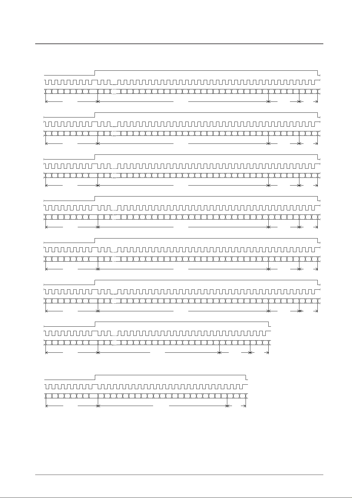
B0 to B3, A0 to A3Note: ······· CCB address
DD································· Direction data
1
PC4 CT0PC2 PC3PC1
0 0 001 10
B1 A1A0B0
1
DI
CL
CE
B3B2 A3A2
CT1
11
BUSCCTCCT3CT2 FC DT1 DT2
0000000
Control
data
21 bits
DD
3 bits
CCB
address
8 bits
No. 7160-8/33
LC75848T
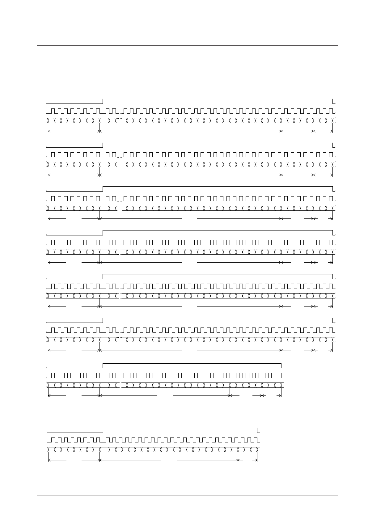
Serial Data Transfer Format
1. 1/8 duty
① When CL is stopped at the low level
• When the display data is transferred.
• When the control data is transferred.
B1 A1A0B0
DI
CL
CE
B3B2 A3A2
B1 A1A0B0 B3B2 A3A2
B1 A1A0B0 B3B2 A3A2
D97 D98 D99 D100 D101 D102 D103 D104 D105 D106 D108D107 D109 D110 D111 D112 D113 D115D114 D116 D117 D118 D119 D120D2D1
Display
data
120 bits
Fixed
data
5 bits
DD
3 bits
CCB
address
8 bits
Display
data
120 bits
Fixed
data
5 bits
DD
3 bits
CCB
address
8 bits
Display
data
120 bits
Fixed
data
5 bits
DD
3 bits
CCB
address
8 bits
D337 D338 D339 D340 D341 D342 D343 D344 D345 D346 D348D347 D349 D350 D351 D352 D353 D355D354 D356 D357 D358 D35900D360
0000
D242D241
0 0001 101
0 0001 101
0 0001 101
01
D217 D218 D219 D220 D221 D222 D223 D224 D225 D226 D228D227 D229 D230 D231 D232 D233 D235D234 D236 D237 D238 D23900D240
0000
D122D121
10
000000 00
B1 A1A0B0 B3B2 A3A2
B1 A1A0B0 B3B2 A3A2
B1 A1A0B0 B3B2 A3A2
D457 D458 D459 D460 D461 D462 D463 D464 D465 D466 D468D467 D469 D470 D471 D472 D473 D475D474 D476 D477 D478 D479 D480D362D361
Display
data
120 bits
Fixed
data
5 bits
DD
3 bits
CCB
address
8 bits
Display
data
120 bits
Fixed
data
5 bits
DD
3 bits
CCB
address
8 bits
Display
data
120 bits
Fixed
data
5 bits
DD
3 bits
CCB
address
8 bits
D697 D698 D699 D700 D701 D702 D703 D704 D705 D706 D708D707 D709 D710 D711 D712 D713 D715D714 D716 D717 D718 D71910D720
0000
D602D601
0 0001 1
D721
1
01
0 0001 101
0 0001 101
10
D577 D578 D579 D580 D581 D582 D583 D584 D585 D586 D588D587 D589 D590 D591 D592 D593 D595D594 D596 D597 D598 D59910D600
0000
D482D481
00
000000 11
B1 A1A0B0 B3B2 A3A2
Display
data
40 bits
Fixed
data
5 bits
DD
3 bits
CCB
address
8 bits
D745 D746 D747 D748 D749 D750 D751 D752 D753 D754 D756D755 D757 D758 D759 D760
0 00 0 0 1 1 0
D722
0 0001 01
1
PC4 CT0PC2PC1 PC3
0 0 001 101
CT1
11
BUSCCTCCT3CT2 FC DT1 DT2
0000000
Control
data
21 bits
DD
3 bits
CCB
address
8 bits
B1 A1A0B0
DI
CL
CE
B3B2 A3A2
B0 to B3, A0 to A3Note:
• CCB address:
• D1 to D760:
• PC1 to PC4:
• CT0 to CT3, CTC:
• SC:
• BU:
• FC:
• DT1, DT2:
83H
Display data
General-purpose output port state setting data
Display contrast setting data
Segment on/off control data
Normal mode/power saving mode control data
Data that sets the frame frequency of the common and segment output waveforms
Display technique setting data
····
········
········
·····················
·····················
·····················
···········
······· CCB address
DD································· Direction data
No. 7160-9/33
LC75848T
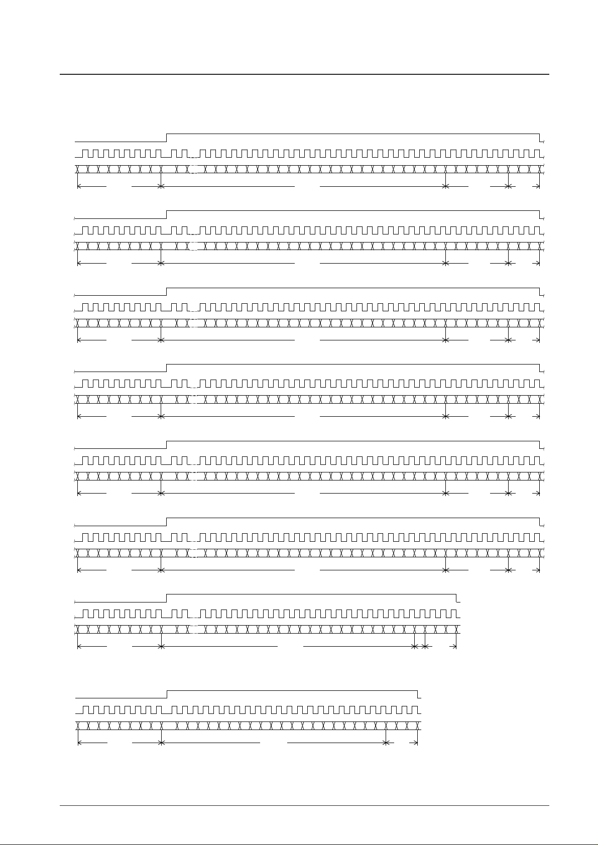
② When CL is stopped at the high level
• When the display data is transferred.
• When the control data is transferred.
No. 7160-10/33
LC75848T
B1 A1A0B0
DI
CL
CE
B3B2 A3A2
B1 A1A0B0 B3B2 A3A2
B1 A1A0B0 B3B2 A3A2
D113 D114 D115 D116 D117 D118 D119 D120 D121 D122 D124D123 D125 D126 D127 D128 D129 D131D130 D132 D133 D134 D135
0
D2D1
Display
data
135 bits
Fixed
data
6 bits
DD
3 bits
CCB
address
8 bits
Display
data
135 bits
Fixed
data
6 bits
DD
3 bits
CCB
address
8 bits
Display
data
135 bits
Fixed
data
6 bits
DD
3 bits
CCB
address
8 bits
D383 D384 D385 D386 D387 D388 D389 D390 D391 D392 D394D393 D395 D396 D397 D398 D399 D401D400 D402 D403 D404 D405
000 0000
D272D271
0 0001 101
0 0001 101
0 0001 101
01
D248 D249 D250 D251 D252 D253 D254 D255 D256 D257 D259D258 D260 D261 D262 D263 D264 D266D265 D267 D268 D269 D270
000 0000
D137D136
10
000000 00
D518 D519 D520 D521 D522 D523 D524 D525 D526 D527 D529D528 D530 D531 D532 D533 D534 D536D535 D537 D538 D539 D540
0
D407D406
Display
data
135 bits
Fixed
data
6 bits
DD
3 bits
CCB
address
8 bits
Display
data
135 bits
Fixed
data
6 bits
DD
3 bits
CCB
address
8 bits
Display
data
135 bits
Fixed
data
6 bits
DD
3 bits
CCB
address
8 bits
D788 D789 D790 D791 D792 D793 D794 D795 D796 D797 D799D798 D800 D801 D802 D803 D804 D806D805 D807 D808 D809 D810
100 0000
D677D676
0 0001 101
0 0001 101
0 0001 101
10
D653 D654 D655 D656 D657 D658 D659 D660 D661 D662 D664D663 D665 D666 D667 D668 D669 D671D670 D672 D673 D674 D675
100 0000
D542D541
00
000000 11
B1 A1A0B0 B3B2 A3A2
B1 A1A0B0 B3B2 A3A2
B1 A1A0B0 B3B2 A3A2
B1 A1A0B0 B3B2 A3A2
B1 A1A0B0
DI
CL
CE
B3B2 A3A2
D811
1
Display
data
36 bits
Fixed
data
1 bits
DD
3 bits
CCB
address
8 bits
D827 D828 D829 D830 D831 D832 D833 D834 D835 D836 D838D837 D839 D840 D841 D842 D843 D845D844 D846
0 1 1 0
D812
0 0001 01
1
PC4 CT0PC2PC1 PC3
0 0 001 101
CT1
11
BUSCCTCCT3CT2 FC DT1 DT2
0000000
Control
data
21 bits
DD
3 bits
CCB
address
8 bits
B0 to B3, A0 to A3Note: ······· CCB address
DD································· Direction data
2. 1/9 duty
① When CL is stopped at the low level
• When the display data is transferred.
• When the control data is transferred.
 Loading...