

Overview
The LC75842E is a 1/2 duty general-purpose LCD display
driver for applications such as microprocessor-controlled
electronic tuning. It can drive up to 54 segments directly.
Features
• 1/2 duty, 1/2 bias drive of up to 54 segments
• Serial data input supports CCB* format communication
with the system controller.
• Backup function which is based on a power saving
mode and all segments off functions that are controlled
by serial data.
• High generality, since display data is displayed directly
without decoder intervention.
• The display can be forced to the off state with the INH
pin.
• RC oscillator circuit
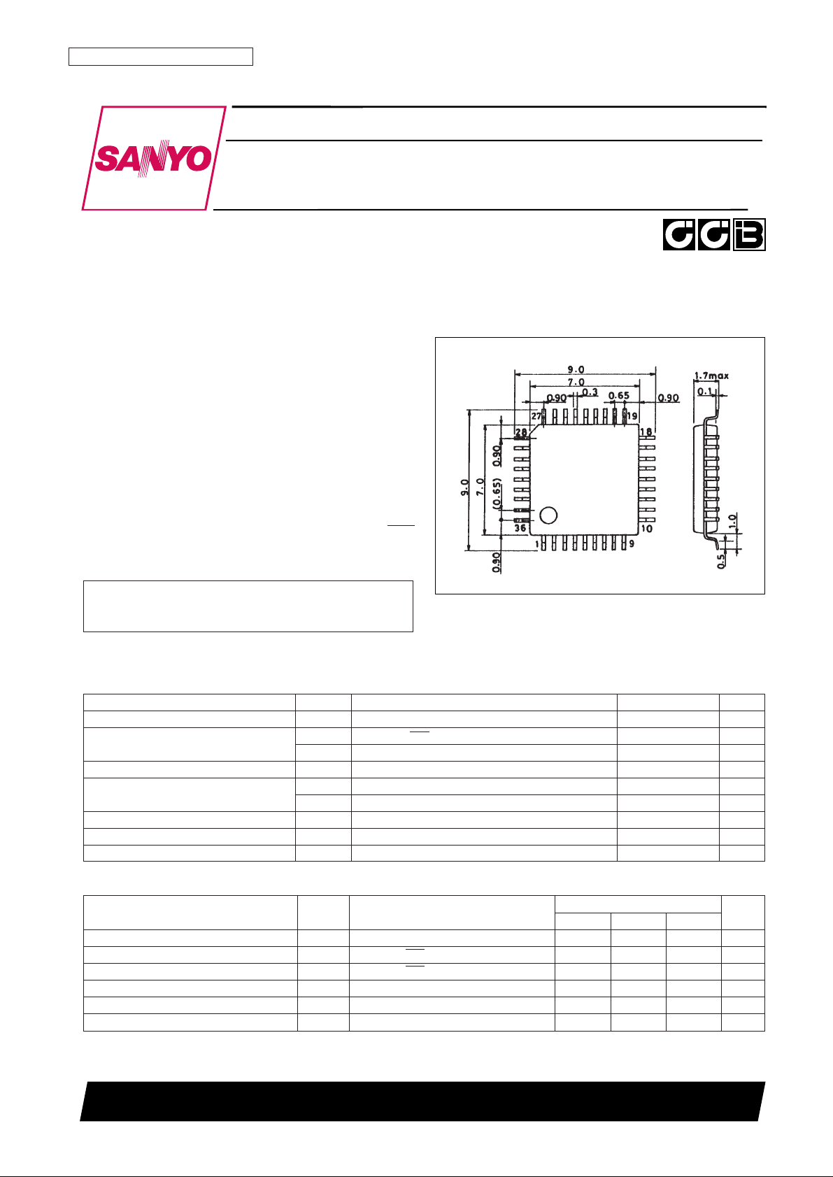
Package Dimensions
unit: mm
3162B-QFP36
CMOS LSI
41096HA (OT)/61595HA (OT) No. 4966-1/9
SANYO: QFP36
[LC75842E]
SANYO Electric Co.,Ltd. Semiconductor Bussiness Headquarters
TOKYO OFFICE Tokyo Bldg., 1-10, 1 Chome, Ueno, Taito-ku, TOKYO, 110 JAPAN
General-Purpose 1/2 Duty LCD Display Driver
LC75842E
Ordering number : EN4966A
• CCB is a trademark of SANYO ELECTRIC CO., LTD.
• CCB is SANYO’s original bus format and all the bus
addresses are controlled by SANYO.
Specifications
Absolute Maximum Ratings at Ta = 25°C, VSS= 0 V
Parameter Symbol Conditions Ratings Unit
Maximum supply voltage V
DD
max V
DD
–0.3 to +6.5 V
Input voltage
V
IN
1 CE, CL, DI, INH –0.3 to +6.5 V
V
IN
2 OSC –0.3 to VDD+ 0.3 V
Output voltage V
OUT
OSC, S1 to S27, COM1, COM2 –0.3 to VDD+ 0.3 V
Output current
I
OUT
1 S1 to S27 100 µA
I
OUT
2 COM1, COM2 1 mA
Allowable power dissipation Pd max Ta = 85°C 100 mW
Operating temperature Topr –40 to +85 °C
Storage temperature Tstg –55 to +125 °C
Parameter Symbol Conditions
Ratings
Unit
min typ max
Supply voltage V
DDVDD
* 4.0 5.0 6.0 V
Input high level voltage V
IH
CE, CL, DI, INH 0.8 V
DD
6.0 V
Input low level voltage V
IL
CE, CL, DI, INH 0 0.2 V
DD
V
Recommended external resistance R
OSC
OSC 68 kΩ
Recommended external capacitance C
OSC
OSC 680 pF
Guaranteed oscillator range f
OSC
OSC 25 50 100 kHz
Allowable Operating Ranges at Ta = –40 to +85°C, VSS= 0 V
Note: * Please contact your Sanyo sales representative if you need to operate the LC75842E at a power supply voltage VDDof 3.0 V (min.).
Continued on next page.
No. 4966-2/9
LC75842E
Continued from preceding page.
Parameter Symbol Conditions
Ratings
Unit
min typ max
Low level clock pulse width t
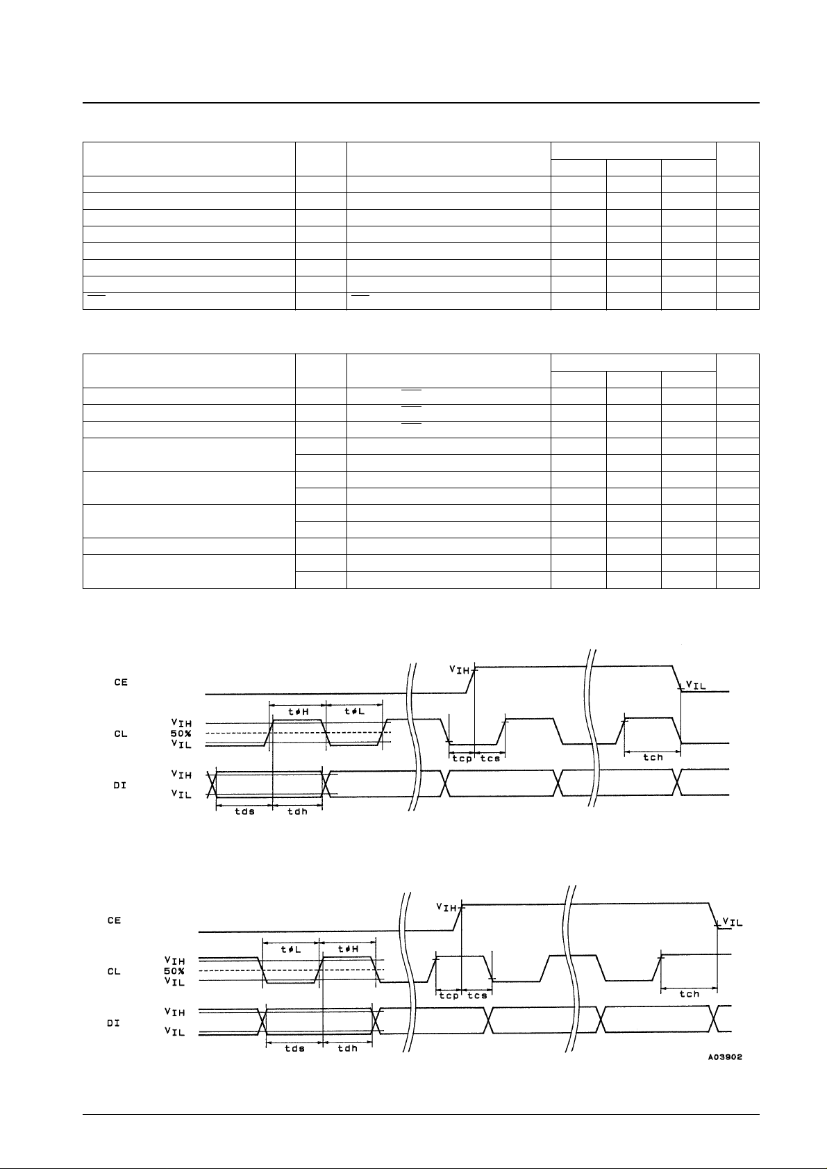
øL
CL: Figure 1 160 ns
High level clock pulse width t
øH
CL: Figure 1 160 ns
Data setup time t
ds
CL, DI: Figure 1 160 ns
Data hold time t
dh
CL, DI: Figure 1 160 ns
CE wait time t
cp
CE, CL: Figure 1 160 ns
CE setup time t
cs
CE, CL: Figure 1 160 ns
CE hold time t
ch
CE, CL: Figure 1 160 ns
INH switching time t
c
INH, CE: Figure 3 10 µs
Parameter Symbol Conditions
Ratings
Unit
min typ max
Hysteresis voltage V
H
CE, CL, DI, INH: VDD= 5.0 V 0.4 V
Input high level current I
IH
CE, CL, DI, INH: VI= 6.0 V 5.0 µA
Input low level current I
IL
CE, CL, DI, INH: VI= 0 V –5.0 µA
Output high level voltage
V
OH
1 S1 to S27: IO= –10 µA VDD– 1.0 V
V
OH
2 COM1, COM2: IO= –100 µA VDD– 0.6 V
Output low level voltage
V
OL
1 S1 to S27: IO= 10 µA 1.0 V
V
OL
2 COM1, COM2: IO= 100 µA 0.6 V
Output middle level voltage
V
MID
1 COM1, COM2: VDD= 6.0 V, IO= ±100 µA 2.4 3.0 3.6 V
V
MID
2 COM1, COM2: VDD= 4.0 V, IO= ±100 µA 1.4 2.0 2.6 V
Oscillator frequency f
OSC
OSC: R
OSC
= 68 kΩ, C
OSC
= 680 pF 40 50 60 kHz
Current drain
I
DD
1 Power saving mode 5 µA
I
DD
2 VDD= 6.0 V, output open, f
OSC
= 50 kHz 1.2 2.0 mA
Electrical Characteristics in the Allowable Operating Ranges
1. When CL is stopped at the low level
2. When CL is stopped at the high level
Figure 1
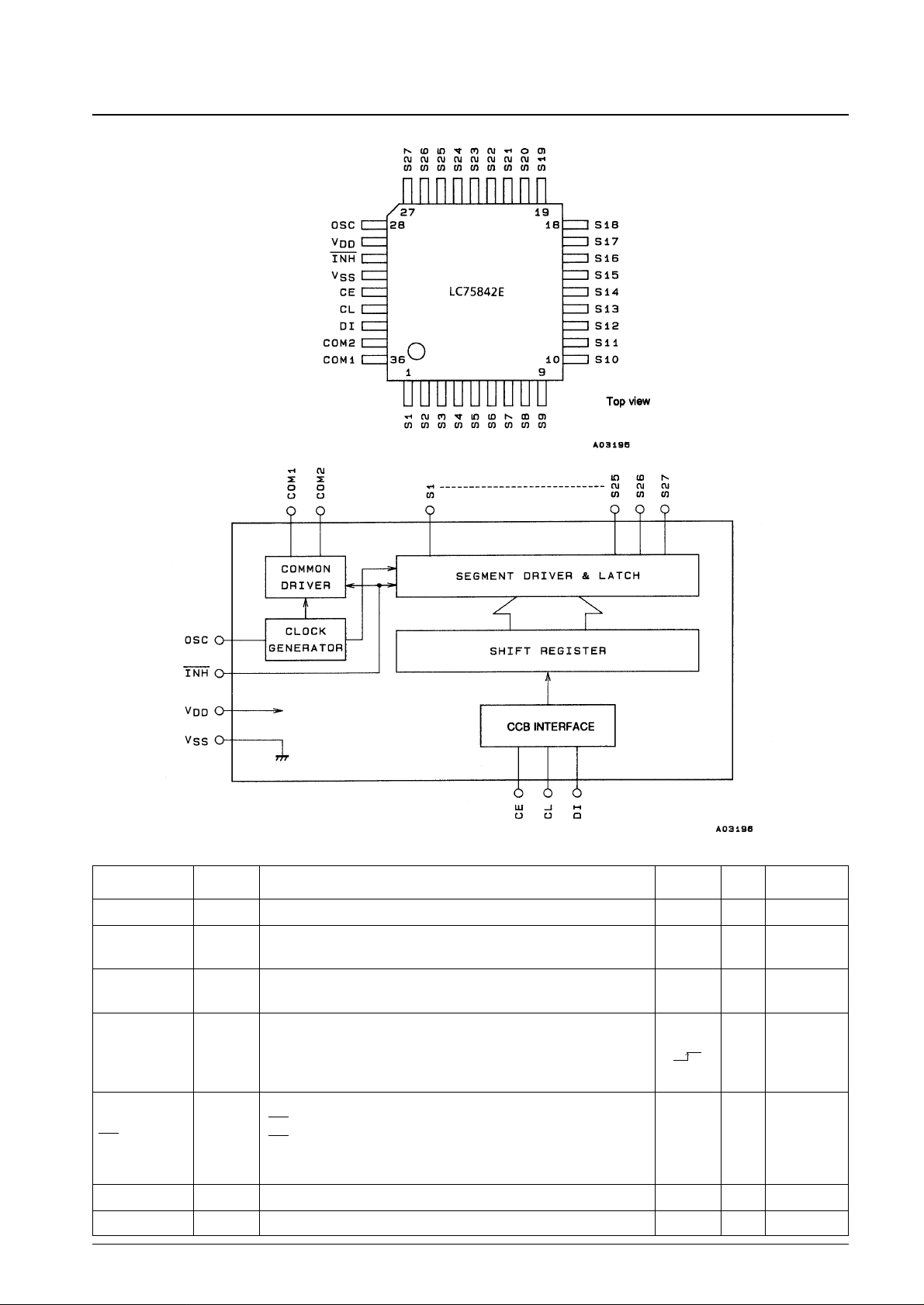
Pin Assignment
No. 4966-3/9
LC75842E
Block Diagram
Pin Pin No. Function Active I/O
Handling when
unused
S1 to S27
COM1
COM2
OSC
CE
CL
DI
INH
V
DD
V
SS
1 to 27
36
35
28
32
33
34
30
29
31
Segment outputs for displaying the display data transferred by serial data input.
Common driver outputs. The frame frequency f
O
is f
OSC
/512 Hz.
Oscillator connection. An oscillator circuit is formed by connecting an external
resistor and capacitor at this pin.
Serial data transfer inputs. Must be connected to the control microprocessor.
CE: Chip enable
CL: Synchronization clock
DI: Transfer data
Display off control input
INH = low (V
SS
).....Display off (S1 to S27, COM1 and COM2 = low)
INH = high (V
DD
)....Display on
However, serial data transfer is possible when the display is forced off by this
pin.
Power supply. Provide a power supply voltage of between 4.0 and 6.0 V.
Power supply. Connect this pin to ground.
—
—
—
L
—
—
H
—
O
O
I/O
I
I
—
—
Open
Open
V
DD
GND
GND
—
—
Pin Functions
 Loading...