

SANYO LC75838W Datasheet

Ordering number : ENN 6902
53101TN (OT) No. 6902-1/32
Overview
The LC75838E and LC75838W are 1/8 to 1/10 duty
general-purpose LCD display drivers used for character
and graphics display. These products operate under the
control of a microcontroller and can directly drive an LCD
with up to 380 segments. They can also control up to 3
general-purpose output ports.
Features
• 1/8duty–1/4bias, 1/9duty–1/4bias, and 1/10duty–1/4bias
drive schemes can be controlled from serial data.
1/8duty–1/4bias: up to 320 segments
1/9duty–1/4bias: up to 351 segments
1/10duty–1/4bias: up to 380 segments
• Serial data input supports CCB format communication
with the system controller.
• Serial data control of the power-saving mode based
backup function and all the segments forced off
function.
• Direct display of display data without the use of a
decoder provides high generality.
• Built-in display contrast adjustment circuit.
• Up to 3 general-purpose output ports are included.
• Independent LCD driver block power supply V
LCD
.
• The INH pin is provided. This pin turns off the display
and forces the general-purpose output ports to the low
level.
• RC oscillator circuit
Package Dimensions
unit: mm
3159-QIP64E
unit: mm
3190-SQFP64
LC75838E, 75838W
SANYO Electric Co.,Ltd. Semiconductor Company
TOKYO OFFICE Tokyo Bldg., 1-10, 1 Chome, Ueno, Taito-ku, TOKYO, 110-8534 JAPAN
1/8 to 1/10 Duty General-Purpose LCD Display Drivers
CMOS IC
Any and all SANYO products described or contained herein do not have specifications that can handle
applications that require extremely high levels of reliability, such as life-support systems, aircraft’s
control systems, or other applications whose failure can be reasonably expected to result in serious
physical and/or material damage. Consult with your SANYO representative nearest you before using
any SANYO products described or contained herein in such applications.
SANYO assumes no responsibility for equipment failures that result from using products at values that
exceed, even momentarily, rated values (such as maximum ratings, operating condition ranges, or other
parameters) listed in products specifications of any and all SANYO products described or contained
herein.
• CCB is a trademark of SANYO ELECTRIC CO., LTD.
• CCB is SANYO’s original bus format and all the bus
addresses are controlled by SANYO.
10.0
12.0
1.25
0.5
1.25
1.25 0.5 1.250.18
12.0
116
17
32
33
48
49
64
10.0
0.5
1.7max
0.5
0.1
0.15
SANYO: SQFP64
[LC75838W]
14.0
17.2
1.0
1.0
1.6
0.15
0.35
0.1
15.6
0.8
0.8
3.0max
1
16
17
32
33
48
49
64
2.7
14.0
17.2
1.0
1.0
1.6
0.8
SANYO: QIP64E
[LC75838E]

No. 6902-2/32
LC75838E, 75838W
Pin Assignment
LC75838E
LC75838W
P1
P2
P3
VDD
VLCD
VLCD0
VLCD1
VLCD2
VLCD3
VLCD4
VSS
OSC
INH
CE
CL
DI
S32
S31
S30
S29
S28
S27
S26
S25
S24
S23
S22
S21
S20
S19
S18
S17
48 33
1 16
3249
1764
COM1
COM2
COM3
COM4
COM5
COM6
COM7
COM8
S40/COM9
S39/COM10
S38
S37
S36
S35
S34
S33
S1S2S3S4S5S6S7S8S9
S10
S11
S12
S13
S14
S15
S16

No. 6902-3/32
LC75838E, 75838W
Parameter Symbol Conditions Ratings Unit
Maximum supply voltage
V
DD
max V
DD
–0.3 to +7.0
V
V
LCD
max V
LCD
–0.3 to +12.0
V
IN
1 CE, CL, DI, INH –0.3 to +7.0
Input voltage V
IN
2 OSC –0.3 to VDD+0.3 V
V
IN
3 V
LCD
1, V
LCD
2, V
LCD
3, V
LCD
4 –0.3 to V
LCD
+0.3
Output voltage
V
OUT
1 OSC, P1 to P3 –0.3 to VDD+0.3
V
V
OUT
2 V
LCD
0, S1 to S40, COM1 to COM10 –0.3 to V
LCD
+0.3
I
OUT
1 S1 to S40 300 µA
Output current I
OUT
2 COM1 to COM10 3
mA
I
OUT
3 P1 to P3 5
Allowable power dissipation Pd max Ta = 85°C 200 mW
Operating temperature Topr –40 to +85 °C
Storage temperature Tstg –55 to +125 °C
Specifications
Absolute Maximum Ratings at Ta=25°C, VSS=0V
Parameter Symbol Conditions
Ratings
Unit
min typ max
V
DDVDD
2.7 6.0
V
LCD
, When the display contrast adjustment 7.0 11.0
Supply voltage
V
LCD
circuit is used V
V
LCD
, When the display contrast adjustment 4.5 11.0
circuit is not used
Output voltage V
LCD
0 V
LCD
0
V
LCD
4 + 4.5
V
LCD
V
V
LCD
1 V
LCD
1
3/4
V
LCD
0
(V
LCD
0–V
LCD
4)
V
LCD
2 V
LCD
2
2/4
V
LCD
0
Input voltage
(V
LCD
0–V
LCD
4)
V
V
LCD
3 V
LCD
3
1/4
V
LCD
0
(V
LCD
0–V
LCD
4)
V
LCD
4 V
LCD
4 0 1.5
Input high level voltage V
IH
CE, CL, DI, INH 0.8 V
DD
6.0 V
Input low level voltage V
IL
CE, CL, DI, INH 0 0.2 V
DD
V
Recommended external resistance R
OSC
OSC 43 kΩ
Recommended external capacitance C
OSC
OSC 680 pF
Guaranteed oscillation range f
OSC
OSC 25 50 100 kHz
Data setup time t
ds
CL, DI :Figure 2 160 ns
Data hold time t
dh
CL, DI :Figure 2 160 ns
CE wait time t
cp
CE, CL :Figure 2 160 ns
CE setup time t
cs
CE, CL :Figure 2 160 ns
CE hold time t
ch
CE, CL :Figure 2 160 ns
High level clock pulse width tø
H
CL :Figure 2 160 ns
Low level clock pulse width tø
L
CL :Figure 2 160 ns
INH switching time t
c
INH, CE :Figures 3, 4, and 5 10 µs
Allowable Operating Ranges at Ta = –40 to +85°C, VSS=0V

No. 6902-4/32
LC75838E, 75838W
Parameter Symbol Conditions
Ratings
Unit
min typ max
Hysteresis V
H
CE, CL, DI, INH 0.1 V
DD
V
Input high level current I
IH
CE, CL, DI, INH: VI= 6.0 V 5.0 µA
Input low level current I
IL
CE, CL, DI, INH: VI= 0 V –5.0 µA
V
OH
1 S1 to S40: IO= –20 µA
V
LCD
0 – 0.6
Output high level voltage VOH2 COM1 to COM10: IO= –100 µA
V
LCD
0 – 0.6
V
V
OH
3 P1 to P3: IO= –1 mA VDD– 1.0
V
OL
1 S1 to S40: IO= 20 µA
V
LCD
4 + 0.6
Output low level voltage VOL2 COM1 to COM10: IO= 100 µA
V
LCD
4 + 0.6
V
V
OL
3 P1 to P3: IO= 1 mA 1.0
2/4 2/4
V
MID
1 S1 to S40: IO= ±20 µA
(V
LCD
0 – V
LCD
4) (V
LCD
0 – V
LCD
4)
–0.6 +0.6
3/4 3/4
Output middle level voltage *1 V
MID
2 COM1 to COM10: IO= ±100 µA
(V
LCD
0 – V
LCD
4) (V
LCD
0 – V
LCD
4)
V
–0.6 +0.6
1/4 1/4
V
MID
3 COM1 to COM10: IO= ±100 µA
(V
LCD
0 – V
LCD
4) (V
LCD
0 – V
LCD
4)
–0.6 +0.6
Oscillator frequency fosc OSC: R
OSC
= 43 kΩ, C
OSC
= 680 pF 40 50 60 kHz
I
DD
1 VDD: Power saving mode 5
I
DD
2 VDD: VDD= 6.0 V,
outputs open, fosc = 50 kHz
200 400
I
LCD
1 V
LCD
: Power saving mode 5
V
LCD
: V
LCD
= 11.0 V
I
LCD
2
Outputs open
500 1000 µA
Current drain
fosc = 50 kHz
When the display contrast adjustment circuit is used.
V
LCD
: V
LCD
= 11.0 V
I
LCD
3
Outputs open
250 500
fosc = 50 kHz
When the display contrast adjustment circuit is not used.
Electrical Characteristics for the Allowable Operating Ranges
Note: *1 Excluding the bias voltage generation divider resistor built into V
LCD
0, V
LCD
1, V
LCD
2 , V
LCD
3, and V
LCD
4. (See Figure 1.)

No. 6902-5/32
LC75838E, 75838W
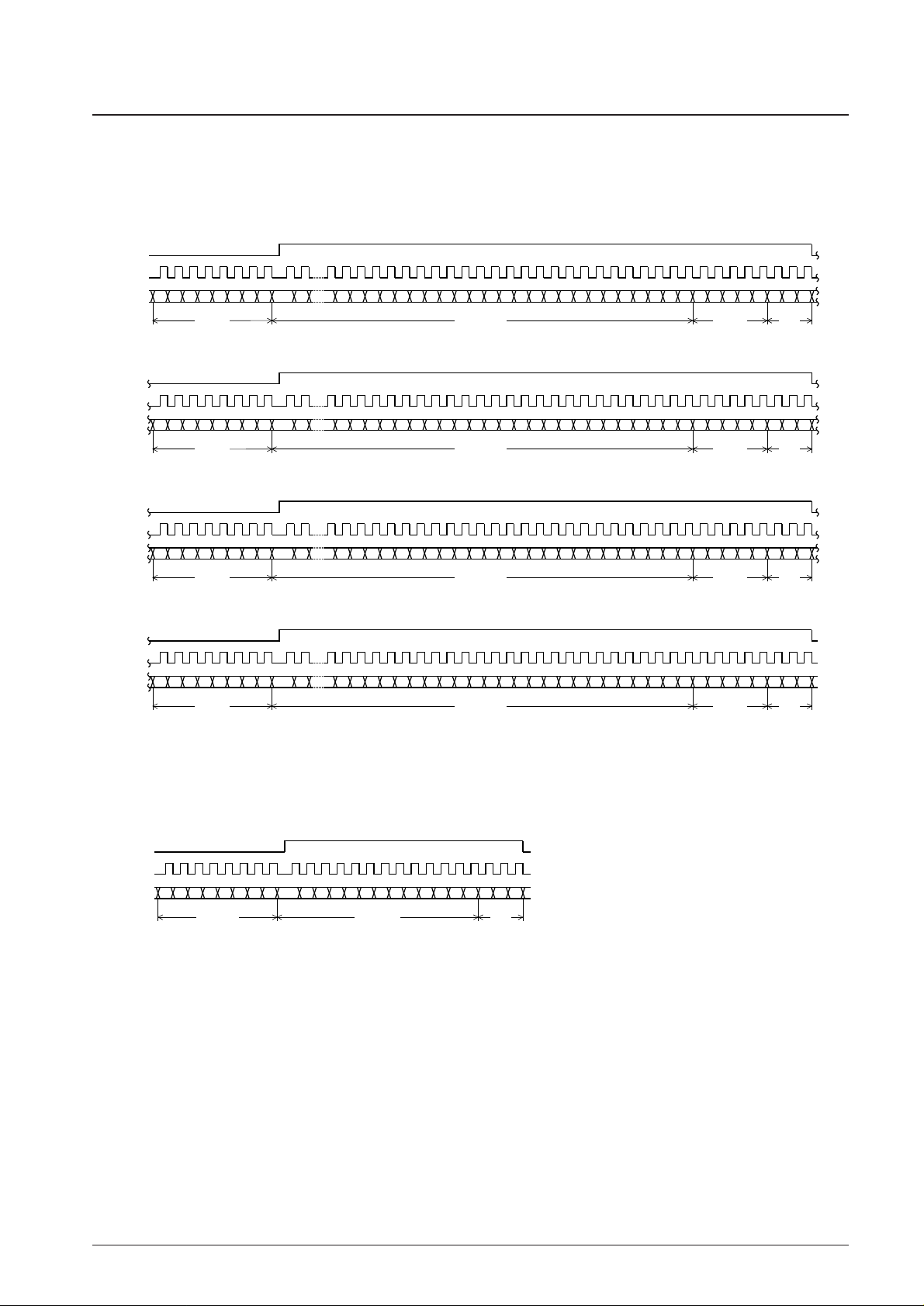
Figure 1
• When CL is stopped at the low level
Figure 2
CE
CL
tøH
tds tdh
tøL
tch
tcstcp
DI
VIH
VIH
VIL
VIH
VIL
VIL
50%
VIH
50%
VIL
VIL
VIH
• When CL is stopped at the high level
CE
CL
tøL
tds tdh
tøH
tchtcstcp
DI
VIH
VIL
VIH
50%
VIL
VIH
VIL
VIH
50%
VIL
VIL
VIH
To the common and segment drivers
Excluding these resistors
CONTRAST
ADJUSTER
No. 6902-6/32
LC75838E, 75838W
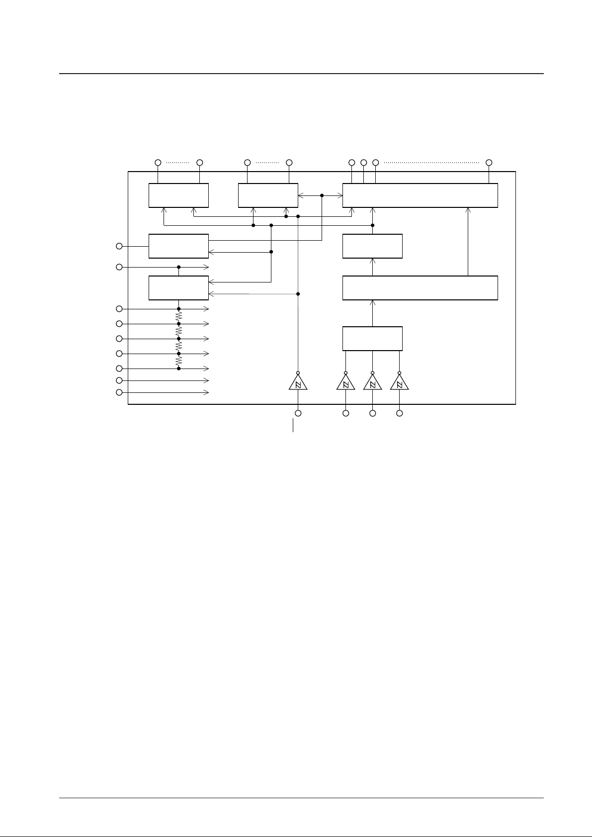
Block Diagram
OSC
VLCD
VLCD0
VLCD1
VLCD2
VLCD3
VLCD4
VDD
VSS
P1
P3
COM1
COM8
S40/COM9
S39/COM10
CE
CL
DI
INH
S38
S1
CCB
INTERFACE
SHIFT REGISTER
CONTROL
REGISTER
SEGMENT DRIVER & LATCH
COMMON
DRIVER
GENERAL
PORT
CLOCK
GENERATOR
CONTRAST
ADJUSTER

No. 6902-7/39
LC75838E, 75838W
Pin Pin No. Function Active I/O
Handling
when unused
S1 to S38 1 to 38 Segment driver outputs.
S39/COM10 39 The S39/COM10 and S40/COM9 pins can be used as common —
●● Open
S40/COM9 40 driver outputs under the control data DT1, DT2.
COM1 to COM8
48 to 41 Common driver outputs. — ●● Open
P1 to P3 49 to 51 General-purpose output ports. — ●● Open
OSC 60 — I/O V
DD
CE 62 H I
CL 63 I GND
DI 64 — I
INH 61 L I GND
V
LCD
0 54 — O Open
V
LCD
1 55 — I Open
V
LCD
2 56 — I Open
V
LCD
3 57 — I Open
V
LCD
4 58 — I GND
V
DD
52 — — —
V
LCD
53 — — —
V
SS
59 Power supply connection. Connect to ground. — — —
Pin Functions
Oscillator connection.
An oscillator circuit is formed by connecting an external resistor and capacitor at this
pin.
Serial data transfer inputs.
These pins are connected to the microcontroller.
CE :Chip enable
CL :Synchronization clock
DI :Transfer data
▲
Input that turns the display off and forces the general-purpose output ports low.
• When INH is low (VSS)
• Display off
S1 to S38 = “L” (V
LCD
4).
S39/COM10, S40/COM9 = “L” (V
LCD
4)
COM1 to COM8 = “L” (V
LCD
4).
• General-purpose output ports P1 to P3 = low (V
SS
)
• When INH is high (V
DD
)
• Display on
• The states of the general-purpose output ports can be set by the PC1 to
PC3 control data.
However, serial data can be transferred when the INH pin is low.
LCD drive 3/4 bias voltage (middle level) supply pin. This pin can be used to supply
the 3/4 (V
LCD
0 – V
LCD
4) voltage level externally.
LCD drive 2/4 bias voltage (middle level) supply pin. This pin can be used to supply
the 2/4 (V
LCD
0 – V
LCD
4) voltage level externally.
LCD drive 1/4 bias voltage (middle level) supply pin. This pin can be used to supply
the 1/4 (V
LCD
0 – V
LCD
4) voltage level externally.
LCD drive 0/4 bias voltage (low level) supply pin. Fine adjustment of the display
contrast can be implemented by connecting an external variable resistor to this pin.
However, (V
LCD
0 – V
LCD
4) must be greater than or equal to 4.5 V, and V
LCD
4 must be
in the range 0 V to 1.5 V, inclusive.
Logic block power supply connection. Provide a voltage of between 2.7 and 6.0V.
LCD driver block power supply connection. Provide a voltage of between 7.0 and 11.0 V
when the display contrast adjustment circuit is used and provide a voltage of between
4.5 and 11.0 V when the circuit is not used.
LCD drive 4/4 bias voltage (high level) supply pin. The level on this pin can be changed
by the display contrast adjustment circuit.
However, (V
LCD
0 – V
LCD
4) must be greater than or equal to 4.5 V. Also,external power
must not be applied to this pin since the pin circuit includes the display contrast
adjustment circuit.
No. 6902-8/32
LC75838E, 75838W
CE
CL
DI
1 0
1
0 0 01 D1
D57 D58 D59 D60 D61 D62 D63 D64 D65 D66 D67 D68 D69 D70 D71 D72 D73 D74 D75 D76 D77 D78 D79 D80 0 0 0 0 0 0 0 0
D21 1
B0 B1
B0
A0
CCB
address
8 bits
Display
data
80 bits
Fixed
data
5 bits
DD
3 bits
A1 A3B2 B3 A2
0
1
0 0 01
D81
D137 D138 D139 D140 D141 D142 D143 D144 D145 D146 D147 D148 D149 D150 D151 D152 D153 D154 D155 D156 D157 D158 D159 D160
0 0 0 0 0 0 0 1D82
1 1
B1
B0
A0
CCB
address
8 bits
Display
data
80 bits
Fixed
data
5 bits
DD
3 bits
A1 A3B2 B3 A2
0
1
0 0 01
D161 D217 D218 D219 D220 D221 D222 D223 D224 D225 D226 D227 D228 D229 D230 D231 D232 D233 D234 D235 D236 D237 D238 D239 D240
0 0 0 0 0 0 1 0
D162
1 1
B1 A0
CCB
address
8 bits
Display
data
80 bits
Fixed
data
5 bits
DD
3 bits
0 0 0 01
D241 D297 D298 D299 D300 D301 D302 D303 D304 D305 D306 D307 D308 D309 D310 D311 D312 D313 D314 D315 D316 D317 D318 D319 D320
0 0 0 0 0 0 1 1
D242
1 1
CCB
address
8 bits
Display
data
80 bits
Fixed
data
5 bits
DD
3 bits
A1 A3B2 B3 A2
B0 B1 A0 A1 A3B2 B3 A2
Serial Data Transfer Format
1. 1/8 duty
① When CL is stopped at the low level
• When the display data is transferred.
• When the control data is transferred.
Note: B0 to B3, A0 to A3
......
CCB address
DD
................................
Direction data
CE
CL
DI
1 0 0 0 0
PC1 PC2 PC3 CT0 CT1 CT2 CT3 CTC SC BU DT1 DT2
0 1 0 01 1 1
CCB
address
8 bits
Control
data
13 bits
DD
3 bits
B0 B1 A0 A1 A3B2 B3 A2
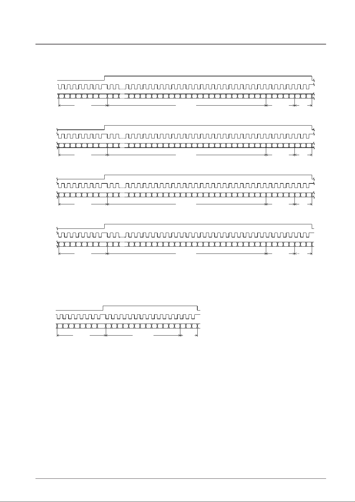
CE
CL
DI
1 0 0 0 0
PC1 PC2 PC3 CT0 CT1 CT2 CT3 CTC SC BU DT1 DT2
0 1 0 01 1 1
CCB
address
8 bits
Control
data
13 bits
DD
3 bits
B0 B1 A0 A1 A3B2 B3 A2
No. 6902-9/32
LC75838E, 75838W
② When CL is stopped at the high level
• When the display data is transferred.
Note: B0 to B3, A0 to A3
......
CCB address
DD
................................
Direction data
• CCB address: ....4DH
• D1 to D320: ........ Display data
• PC1 to PC3: ........ General-purpose output port state setting data
• CT0 to CT3, CTC: Display contrast setting data
• SC: ...................... Segment on/off control data
• BU: ...................... Normal mode/power saving mode control data
• DT1, DT2:............ Display technique setting data
CE
CL
DI
1 0 0 0 01 D1
D57 D58 D59 D60 D61 D62 D63 D64 D65 D66 D67 D68 D69 D70 D71 D72 D73 D74 D75 D76 D77 D78 D79 D80 0 0 0 0 0 0 0 0
D21 1
B0 B1 A0
CCB
address
8 bits
Display
data
80 bits
Fixed
data
5 bits
DD
3 bits
A1 A3B2 B3 A2
1B00 0 0 01
D81
D137 D138 D139 D140 D141 D142 D143 D144 D145 D146 D147 D148 D149 D150 D151 D152 D153 D154 D155 D156 D157 D158 D159 D160
0 0 0 0 0 0 0 1D82
1 1
B1 A0
CCB
address
8 bits
Display
data
80 bits
Fixed
data
5 bits
DD
3 bits
A1 A3B2 B3 A2
1B00 0 0 01
D161 D217 D218 D219 D220 D221 D222 D223 D224 D225 D226 D227 D228 D229 D230 D231 D232 D233 D234 D235 D236 D237 D238 D239 D240
0 0 0 0 0 0 1 0
D162
1 1
B1 A0
CCB
address
8 bits
Display
data
80 bits
Fixed
data
5 bits
DD
3 bits
A1 A3B2 B3 A2
1 0 0 0 01
D241 D297 D298 D299 D300 D301 D302 D303 D304 D305 D306 D307 D308 D309 D310 D311 D312 D313 D314 D315 D316 D317 D318 D319 D320
0 0 0 0 0 0 1 1
D242
1 1
CCB
address
8 bits
Display
data
80 bits
Fixed
data
5 bits
DD
3 bits
B0 B1 A0 A1 A3B2 B3 A2
• When the control data is transferred.

No. 6902-10/32
LC75838E, 75838W
CE
CL
DI
1 0
1
0 0 01 D1
D65 D66 D67 D68 D69 D70 D71 D72 D73 D74 D75 D76 D77 D78 D79 D80 D81 D82 D83 D84 D85 D86 D87 D88 D89 D90 0 0 0 0 0 0
D21 1
B0 B1
B0
A0
CCB
address
8 bits
Display
data
90 bits
Fixed
data
3 bits
DD
3 bits
A1 A3B2 B3 A2
0
1
0 0 01
D91
D155 D156 D157 D158 D159 D160 D161 D162 D163 D164 D165 D166 D167 D168 D169 D170 D171 D172 D173 D174 D175 D176 D177 D178 D179 D180
0 0 0 0 0 1D92
1 1
B1
B0
A0
CCB
address
8 bits
Display
data
90 bits
Fixed
data
3 bits
DD
3 bits
A1 A3B2 B3 A2
0
1
0 0 01
D181 D245 D246 D247 D248 D249 D250 D251 D252 D253 D254 D255 D256 D257 D258 D259 D260 D261 D262 D263 D264 D265 D266 D267 D268 D269 D270
0 0 0 0 1 0
D182
1 1
B1 A0
CCB
address
8 bits
Display
data
90 bits
Fixed
data
3 bits
DD
3 bits
0 0 0 01
D271 D335 D336 D337 D338 D339 D340 D341 D342 D343 D344 D345 D346 D347 D348 D349 D350 D351
0 0 0 0 0 0 0 0 0 0 0 0 0 1 1
D272
1 1
CCB
address
8 bits
Display
data
81 bits
Fixed
data
12 bits
DD
3 bits
A1 A3B2 B3 A2
B0 B1 A0 A1 A3B2 B3 A2
2. 1/9 duty
① When CL is stopped at the low level
• When the display data is transferred.
• When the control data is transferred.
Note: B0 to B3, A0 to A3
......
CCB address
DD
................................
Direction data
CE
CL
DI
1 0 0 0 0
PC1 PC2 PC3 CT0 CT1 CT2 CT3 CTC SC BU DT1 DT2
0 1 0 01 1 1
CCB
address
8 bits
Control
data
13 bits
DD
3 bits
B0 B1 A0 A1 A3B2 B3 A2
 Loading...