SANYO LC75395E Datasheet
Specifications
Absolute Maximum Ratings at Ta = 25°C, VSS= 0 V
CMOS LSI
Ordering number : EN5056A
63096HA (OT)/71895HA (OT) No. 5056-1/17
SANYO Electric Co.,Ltd. Semiconductor Bussiness Headquarters
TOKYO OFFICE Tokyo Bldg., 1-10, 1 Chome, Ueno, Taito-ku, TOKYO, 110 JAPAN
Single-Chip Electronic Volume Control System
LC75395E
Overview
The LC75395E is an electronic volume control that
provides volume, balance, five-band equalization and
input switching functions. These functions are controlled
from serial input data.
Functions
• Volume control: The volume control provides 25
attenuation positions: from 0 dB to –17.5 dB in 1.25 dB
steps, from –17.5 dB to –25 dB in 2.5 dB steps, from
–25 dB to –36.25 dB in 3.75 dB steps and with settings
for –41.25 dB, –50 dB, –60 dB and –∞.
A balance function can be implemented by controlling
the left and right channels independently.
• Equalizer: The equalizer function supports ±10 dB
control in 2 dB steps in each of the five bands. Of the
five bands, four provide peaking characteristics, and one
provides shelving characteristics.
• Selector: The selector function selects one of four inputs
for each of the left and right channels. An arbitrary
amplification level can be set for each input signal using
external components.
• Serial data input: All controls can be set from serial
input data (CCB format)
Features
• On-chip buffer amplifiers to minimize the number of
external components
• Silicon-gate CMOS process for minimal switching noise
• On-chip circuit to generate the VDD/2 reference voltage
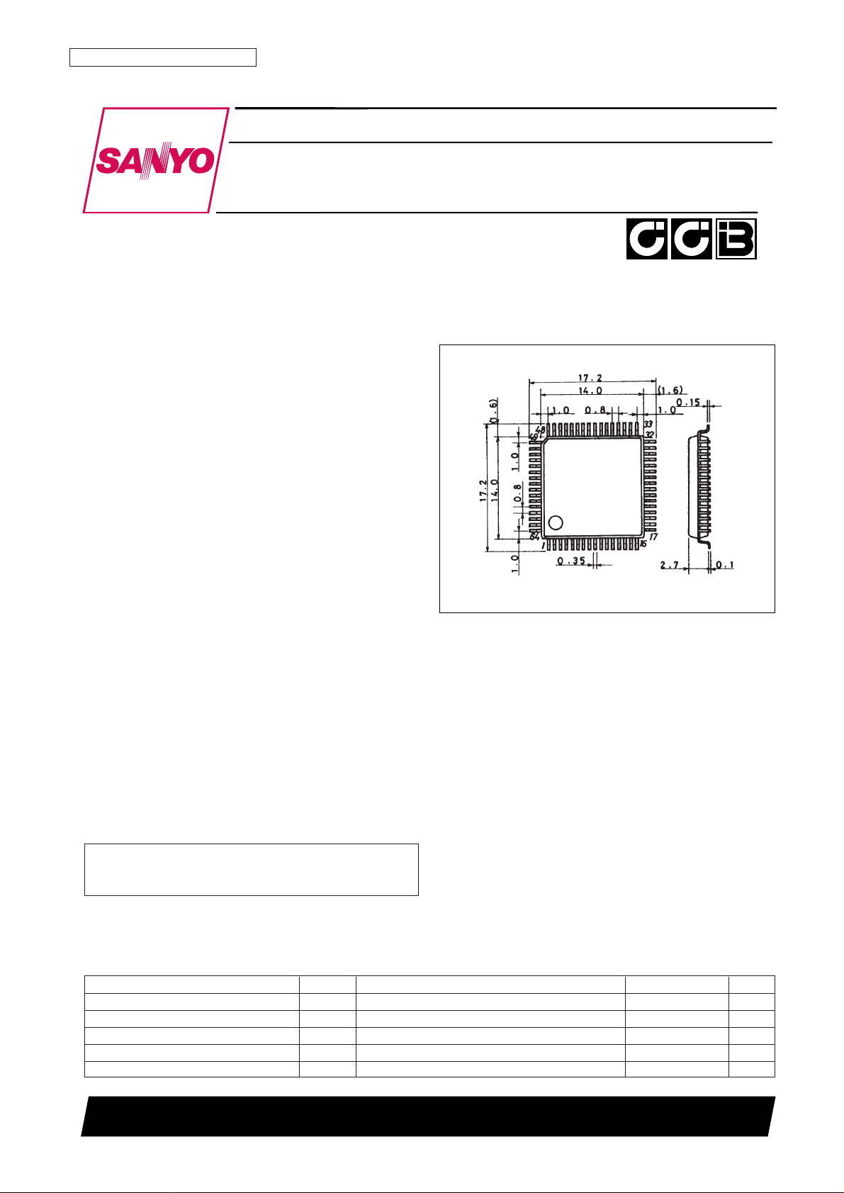
Package Dimensions
unit: mm
3159-QFP64E
• CCB is a trademark of SANYO ELECTRIC CO., LTD.
• CCB is SANYO’s original bus format and all the bus
addresses are controlled by SANYO.
Parameter Symbol Conditions Ratings Unit
Maximum supply voltage V
DD
max V
DD
12 V
Maximum input voltage V
IN
max CL, DI, CE, L1 to L4, R1 to R4, LTIN, RTIN, LVRIN, RVRIN VSS– 0.3 to VDD+ 0.3 V
Allowable power dissipation Pd max Ta ≤ 85°C 310 mW
Operating temperature Topr –30 to +85 °C
Storage temperature Tstg –40 to +125 °C
[LC75395E]
SANYO: QIP64E
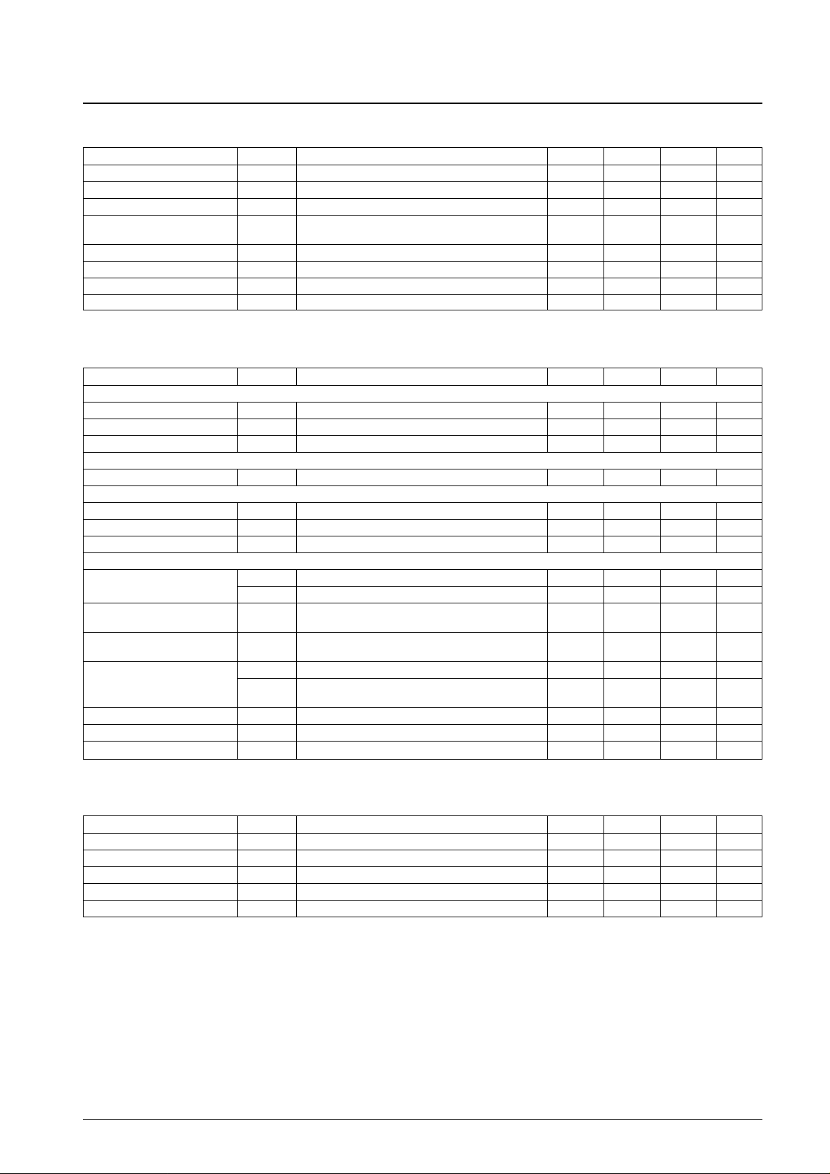
Allowable Operating Ranges at Ta = 25°C, VSS= 0 V
Electrical Characteristics at Ta = 25°C, VDD= 10 V, VSS= 0 V
Input Amplifier Characteristics at Ta = 25°C, VDD– VSS= 10 V
No. 5056-2/17
LC75395E
Parameter Symbol Conditions min typ max Unit
Supply voltage V
DD
V
DD
6.0 11.0 V
Input high level voltage V
IH
CL, DI, CE 4.0 V
DD
V
Input low level voltage V
IL
CL, DI, CE V
SS
1.0 V
Input voltage amplitude V
IN
CL, DI, CE, L1 to L4, R1 to R4, LTIN, RTIN,
V
SS
V
DD
Vp-p
LVRIN, RVRIN
Input pulse width t
øW
CL 1.0 µs
Setup time t
SETUP
CL, DI, CE 1.0 µs
Hold time t
HOLD
CL, DI, CE 1.0 µs
Operating frequency fopg CL 500 kHz
Parameter Symbol Conditions min typ max Unit
[Input Block]
Input resistance Rin L1 to L4, R1 to R4 1 MΩ
Clipping level Vcl LSELO, RSELO: THD = 1.0% 2.65 Vrms
Output load resistance R
L
LSELO, RSELO 3 kΩ
[Volume Control Block]
Input resistance Rin LVRIN, RVRIN 21 35 49 kΩ
[Equalizer Control Block]
Control range Geq Max, boost/cut ±8 ±10 ±12 dB
Step resolution Estep 1 2 3 dB
Internal feedback resistance Rfeed 17 28 39 kΩ
[Overall Characteristics]
Total harmonic distortion
THD (1) V
IN
= 1 Vrms, f = 1 kHz, with all controls flat overall 0.0033 %
THD (2) V
IN
= 1 Vrms, f = 20 kHz, with all controls flat overall 0.012 %
Crosstalk CT
V
IN
= 1 Vrms, f = 1 kHz, with all controls flat overall
86 dB
Rg = 1 kΩ
Output at maximum attenuation V
O
min
V
IN
= 1 Vrms, f = 1 kHz, with the main volume
–84 dB
control at –∞
V
N
(1) With all controls flat overall (IHF-A), Rg = 1 kΩ 3.9 µV
Output noise voltage
V
N
(2)
With all controls flat overall (DIN-AUDIO),
5.4 µV
Rg = 1 kΩ
Current drain I
DD
VDD– VSS= 11 V 25 33 mA
Input high level current I
IH
CL, DI, CE: VIN= 11 V 10 µA
Input low level current I
IL
CL, DI, CE: VIN= 0 V –10 µA
Parameter Symbol Conditions min typ max Unit
Input offset voltage V
IO
–10 +10 mV
Input offset current I
IO
VSS≤ VIN≤ V
DD
±10 nA
Open-loop voltage gain A
O
80 dB
0 dB bandwidth f
T
2.5 MHz
Allowable load resistance R
L
3 kΩ
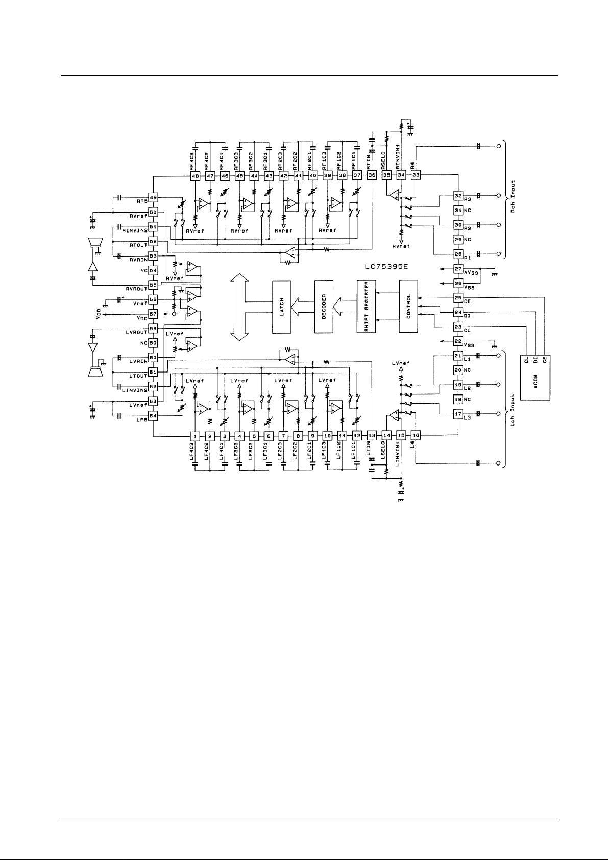
Equivalent Circuit Block Diagram and Sample Application Circuit
Note: If at all possible, use bipolar capacitors for all capacitors that do not have a polarity specified.
No. 5056-3/17
LC75395E
A03544
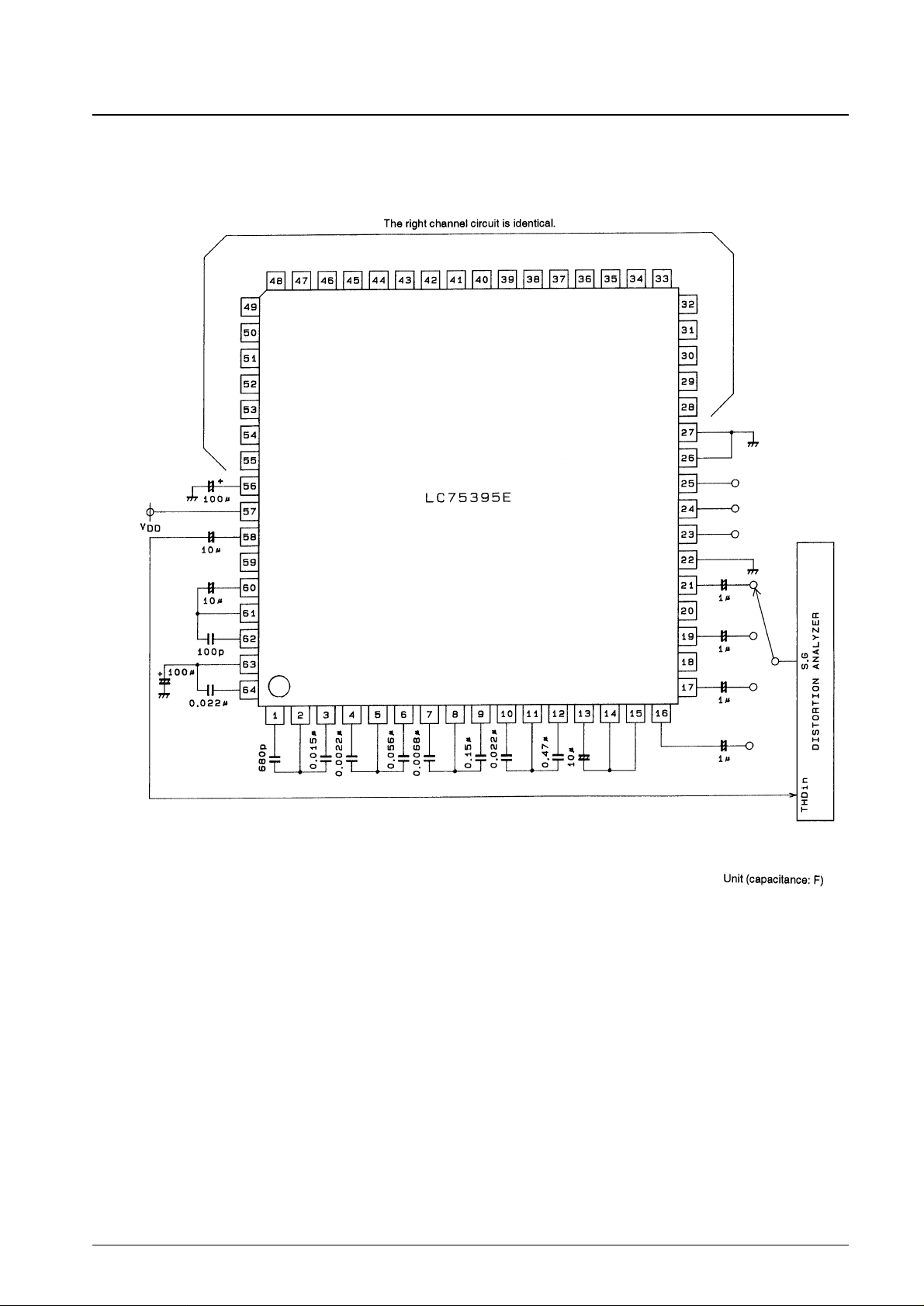
Test Circuits
1. Total Harmonic Distortion
No. 5056-4/17
LC75395E
A03545
Test Circuits
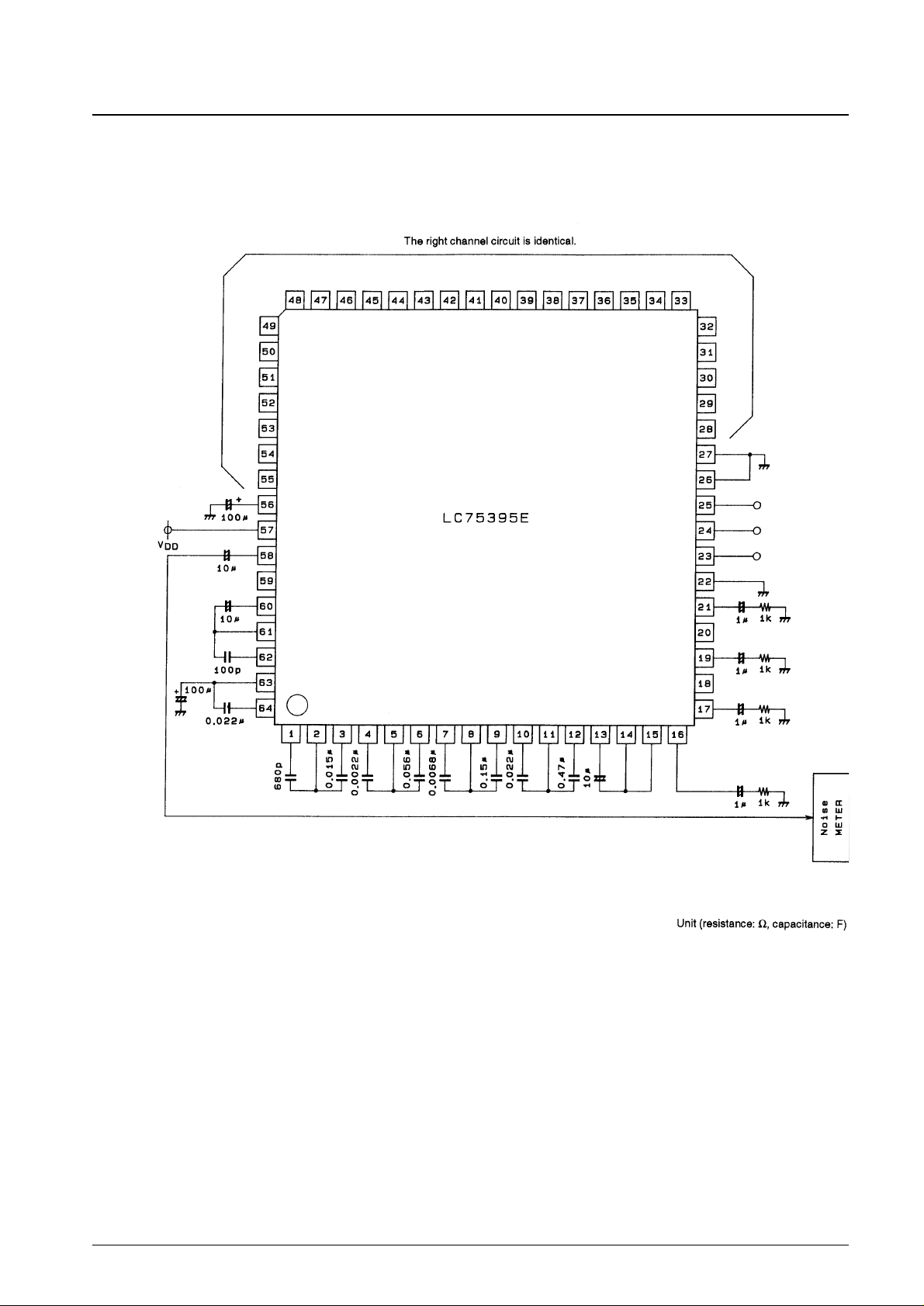
2. Output Noise Voltage
No. 5056-5/17
LC75395E
A03546
Test Circuits
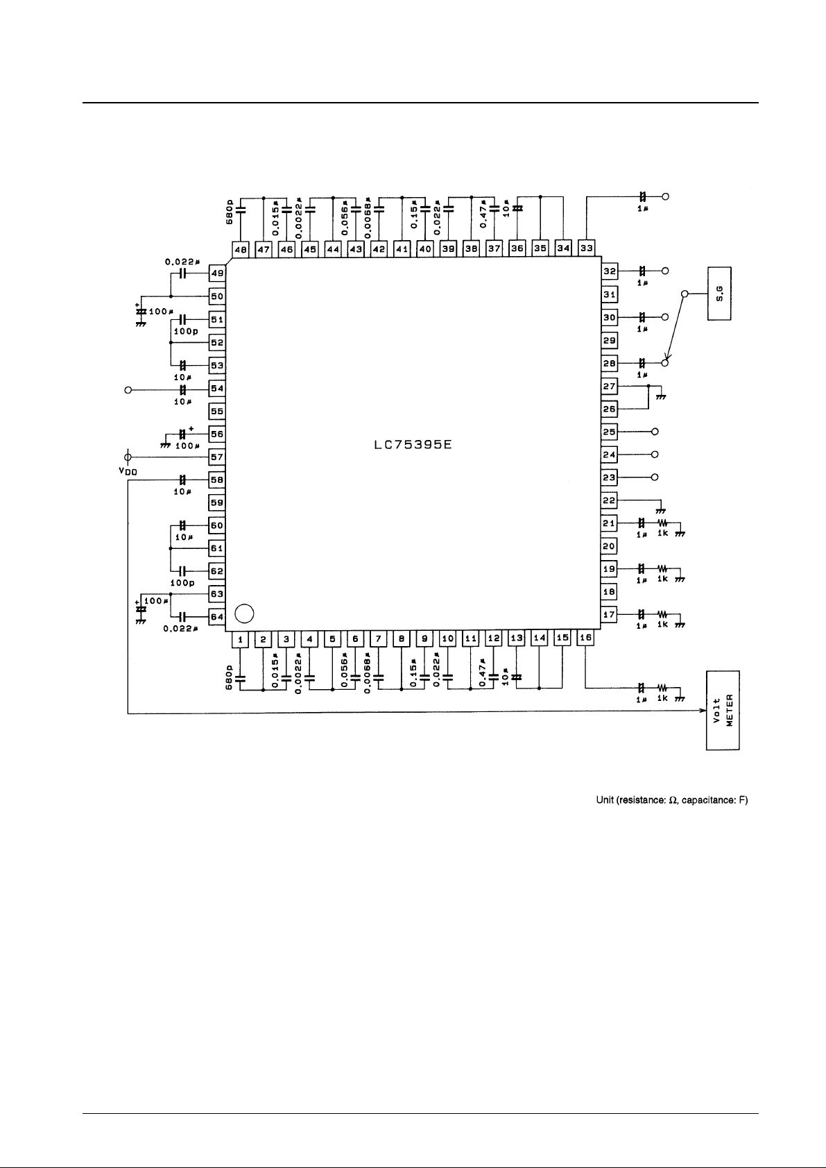
3. Crosstalk
No. 5056-6/17
LC75395E
A03547
 Loading...