

Page 1

Overview
The LC75386NE-R and 75386NW are electronic volume
and tone control ICs that can implement volume, balance,
fader, bass/treble, loudness, input switching, and input
gain control functions with a minimum number of external
components.
Features
• Volume: 81 positions: from 0 dB to –79 dB in 1-dB steps
and –∞.
A balance function can be implemented by
controlling the left and right volume settings
independently.
• Fader: Either the rear or front outputs can be attenuated
over 16 positions. (16 positions: From 0 dB to
–2 dB in 1-dB steps, from –2 dB to –20 dB in
2-dB steps, from –20 to –30 dB in one 10-dB step,
–45 dB, –60 dB, and –∞.)
• Bass/treble: Control over ±12 dB in 2-dB steps in each
band.
• Input gain: The input signal can be amplified by from 0
dB to +18.75 dB in 1.25-dB steps.
• Input switching: The left and right channels can each be
selected from one of 6 inputs. (Five are
single-ended inputs and one is a
differential input.)
• Loudness: Taps are output from a 2-dB step volume
control ladder resistor starting at the –32-dB
position. A loudness function can be
implemented by attaching external capacitors
and resistors.
• On-chip buffer amplifiers minimize the number of
required external components.
• Minimal switching noise when no input signals are
present due to fabrication in a silicon gate CMOS
process that minimizes the noise generated by internal
switches.
• Use of zero-cross switching circuits for internal switches
minimizes switching noise when signals are present.
• Built-in VDD/2 reference voltage generator circuit
• All controls can be set from serial input data.
CMOS IC
33000TN (OT) No.6170-1/24
SANYO Electric Co.,Ltd. Semiconductor Company
TOKYO OFFICE Tokyo Bldg., 1-10, 1 Chome, Ueno, Taito-ku, TOKYO, 110-8534 JAPAN
Electronic Volume and Tone Control
for Car Stereo Systems
LC75386NE-R, 75386NW
Ordering number : ENN6170
• CCB is a trademark of SANYO ELECTRIC CO., LTD.
• CCB is SANYO’s original bus format and all the bus
addresses are controlled by SANYO.
Any and all SANYO products described or contained herein do not have specifications that can handle
applications that require extremely high levels of reliability, such as life-support systems, aircraft’s
control systems, or other applications whose failure can be reasonably expected to result in serious
physical and/or material damage. Consult with your SANYO representative nearest you before using
any SANYO products described or contained herein in such applications.
SANYO assumes no responsibility for equipment failures that result from using products at values that
exceed, even momentarily, rated values (such as maximum ratings, operating condition ranges, or other
parameters) listed in products specifications of any and all SANYO products described or contained
herein.
Page 2
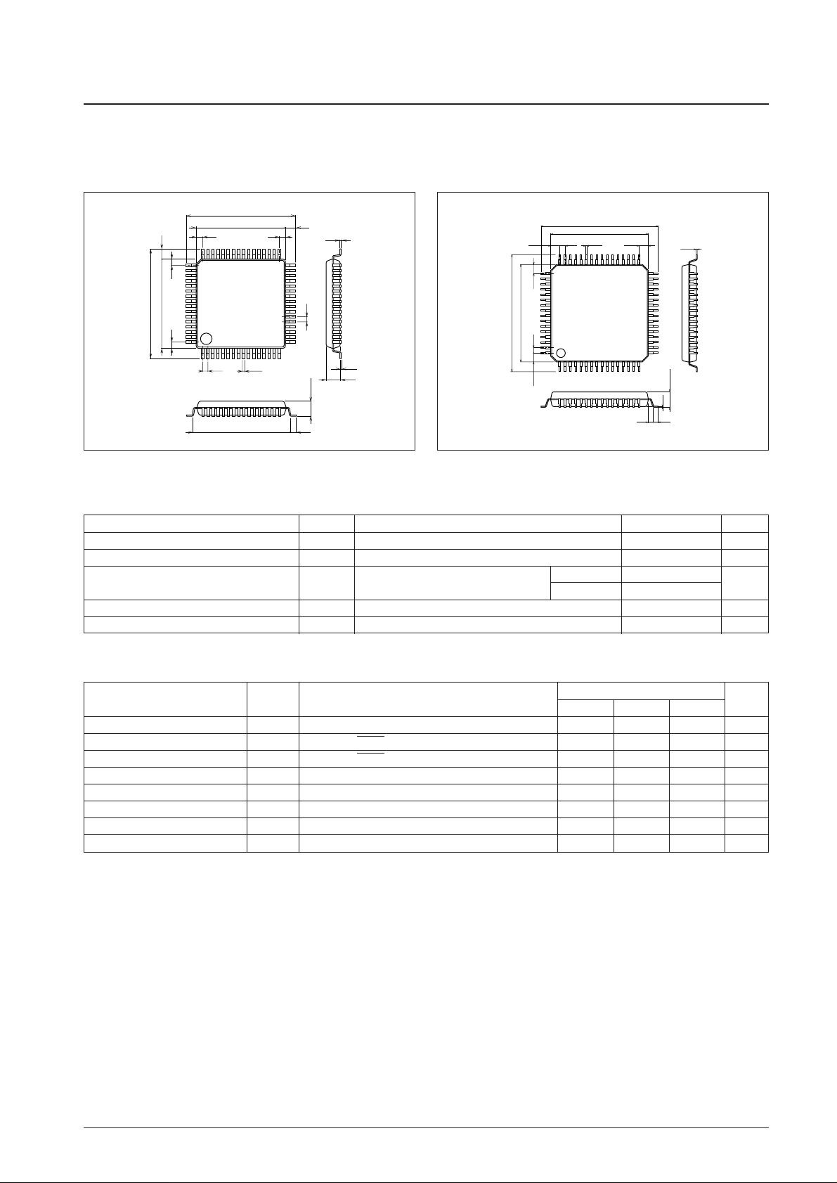
No.6170-2/24
LC75386NE-R, 75386NW
14.0
17.2
1.0
1.0
1.6
0.15
0.35
0.1
15.6
0.8
0.8
3.0max
1
16
17
32
33
48
49
64
2.7
14.0
17.2
1.0
1.0
1.6
0.8
SANYO: QIP64E
[LC75386NE-R]
10.0
12.0
1.25
0.51.25
1.25 0.5 1.250.18
12.0
116
17
32
33
48
49
64
10.0
0.5
1.7max
0.5
0.1
0.15
SANYO: SQFP64E
[LC75386NW]
Package Dimensions
unit: mm
3159-QIP64E 3190-SQFP64
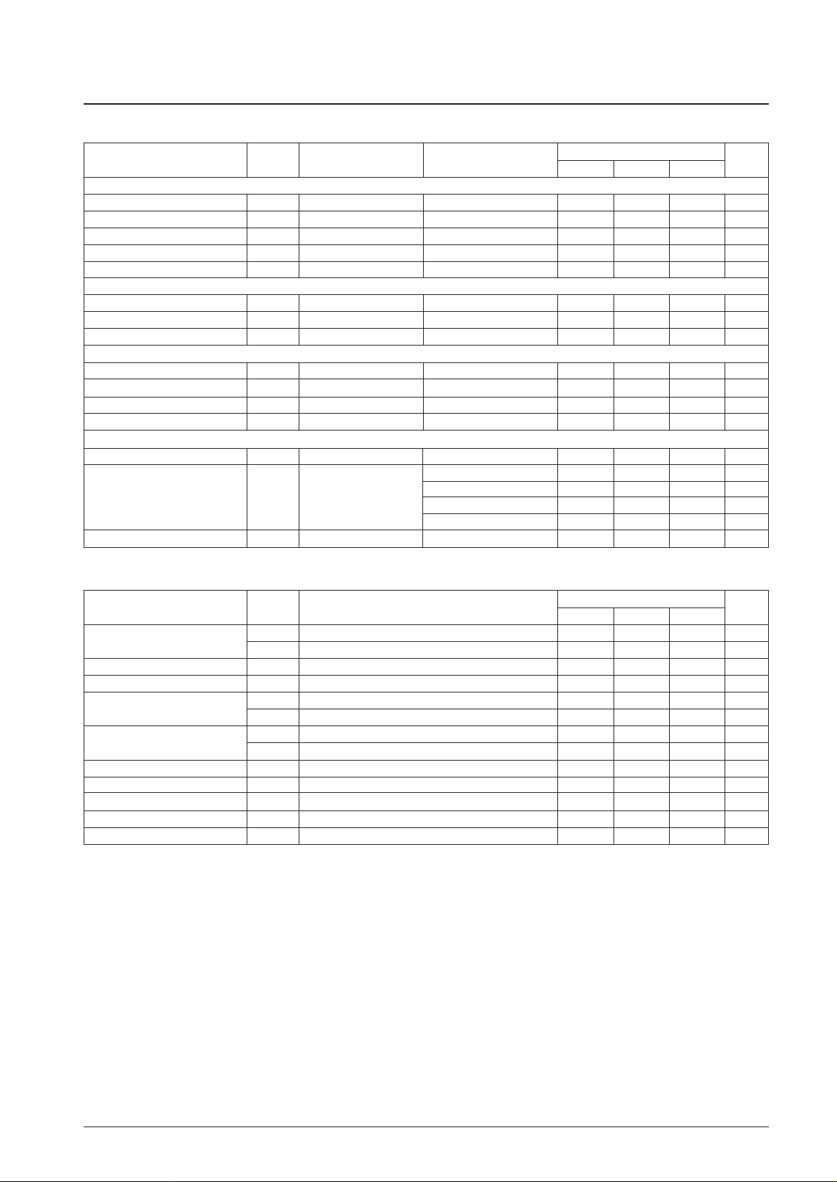
Parameter Symbol Conditions
Ratings
Unit
min typ max
Supply voltage V
DD
V
DD
6.0 10.5 V
Input high-level voltage V
IH
CL, DI, CE, MUTE 4.0 V
DD
V
Input low-level voltage V
IL
CL, DI, CE, MUTE V
SS
1.0 V
Input voltage amplitude V
IN
V
SS
V
DD
Vp-p
Input pulse width t
øW
CL 1 µs
Setup time t
setup
CL, DI, CE 1 µs
Hold time t
hold CL, DI, CE 1 µs
Operating frequency fopg CL 500 kHz
Allowable Operating Ranges at Ta = 25°C, VSS= 0 V
Parameter Symbol Conditions Ratings Unit
Maximum supply voltage V
DD
max V
DD
11 V
Maximum input voltage V
IN
max All input pins
VSS– 0.3 to VDD+ 0.3
V
Allowable power dissipation Pd max
Ta ≤ 85°C, when mounted on a printed
LC75386NE-R 500
mW
circuit board
LC75386NW 420
Operating temperature Topr –40 to +85 °C
Storage temperature Tstg –50 to +125 °C
Specifications
Absolute Maximum Ratings at Ta = 25°C, VSS= 0 V
Page 3
No.6170-3/24
LC75386NE-R, 75386NW
Parameter Symbol Pins Conditions
Ratings
Unit
min typ max
[Input Block]
Input resistance Rin L1 to L4, L6, R1 to R4, R6 30 50 70 kΩ
Minimum input gain Ginmin L1 to L4, L6, R1 to R4, R6 –1 0 +1 dB
Maximum input gain Ginmax +16.5 +18.75 +21 dB
Inter-step setting error ATerr ±0.6 dB
Left/right balance BAL ±0.5 dB
[Volume Block]
Input resistance Rvr
LVRIN, RVRIN, loudness off
113 226 339 kΩ
Inter-step setting error ATerr ±0.5 dB
Left/right balance BAL ±0.5 dB
[Tone Control Block]
Inter-step setting error ATerr ±1.0 dB
Bass control range Gbass max. boost/cut ±9 ±12 ±15 dB
Treble control range Gtre max. boost/cut ±9 ±12 ±15 dB
Left/right balance BAL ±0.5 dB
[Fader Block]
Input resistance Rfed LFIN, RFIN 25 50 100 kΩ
0 dB to –2 dB ±0.5 dB
Inter-step setting error ATerr
–2 dB to –20 dB ±1 dB
–20 dB to –30 dB ±2 dB
–30 dB to –60 dB ±3 dB
Left/right balance BAL ±0.5 dB
Electrical Characteristics at Ta = 25°C, VDD= 9 V, VSS= 0 V
Overall Characteristics
Parameter Symbol Conditions
Ratings
Unit
min typ max
Total harmonic distortion
THD 1 V
IN
= –10 dBV, f = 1 kHz 0.004 %
THD 2 V
IN
= –10 dBV, f = 10 kHz 0.006 %
Inter-input crosstalk CT V
IN
= 1 Vrms, f = 1 kHz 80 88 dB
Left/right channel crosstalk CT V
IN
= 1 Vrms, f = 1 kHz 80 88 dB
Maximum attenuation
V
O
min 1 V
IN
= 1 Vrms, f = 1 kHz 80 88 dB
V
O
min 2 V
IN
= 1 Vrms, f = 1 kHz, INMUTE, with the fader set to –∞ 90 95 dB
Output noise voltage
V
N
1 All controls flat, with the IHF-A filter 5 10 µV
V
N
2 All controls flat, with a 20 Hz to 20 kHz bandpass filter 7 15 µV
Current drain I
DD
33 40 mA
Input high-level current I
IH
CL, DI, CE, VIN= 9 V 10 µA
Input low-level current I
IL
CL, DI, CE, VIN= 0 V –10 µA
Maximum input voltage V
CL
THD = 1 %, RL= 10 kΩ, all controls flat, fIN= 1 kHz 2.5 2.9 Vrms
Common-mode rejection ratio CMRR V
IN
= 0 dB, f = 1 kHz 45 dB
Page 4

No.6170-4/24
LC75386NE-R, 75386NW
Pin Assignment
34 333536373839404142434445464748
3249
31
30
29
28
27
26
25
24
23
22
21
20
19
18
17
41 2 3 5 6 7 8 9 10 11 12 13 14 15 16
50
51
52
53
54
55
56
57
58
59
60
61
62
63
64
LTOUT
LF3C3
LF3C2
LF3C1
NC
NC
NC
LF1C3
LF1C2
LF1C1
LTIN
LVROUT
LCOM
LCT
LVRIN
LSELO
L5P LFIN
L5M LFOUT
L4 LROUT
L3 LAV
SS
L2 LZCLP
L1 DV
SS
L6 CL
LC75386NE-R
LC75386NW
V
DD
DI
Vref CE
R6 MUTE
R1 RAV
SS
R2 RZCLP
R3 TIM
R4 RROUT
R5M RFOUT
R5P RFIN
(Top view)
RSELO
RVRIN
RCT
RCOM
RVROUT
RTIN
RF1C1
RF1C2
RF1C3
NC
NC
NC
RF3C1
RF3C2
RF3C3
RTOUT
200
0
400
600
800
1000
1200
1040
500
1400
–40 –20 0 20 40 60 80 100
420
200
200
0
400
600
800
1000
1200
1400
–40 –20 0 20 40 60 80 100
Allowable power dissipation, Pdmax — mW
Ambient temperature, Ta — °C
Mounted on the printed circuit board
Independent IC
Printed circuit board: 114.3 × 76.2 × 1.5 mm
Pd max — Ta
[LC75386NE-R] [LC75386NW]
Allowable power dissipation, Pdmax — mW
Pd max — Ta
Ambient temperature, Ta — °C
Mounted on the stipulated printed circuit board
Independent IC
Printed circuit board size: 114.3 × 76.1 × 1.6t mm
Printed circuit board material: Fiberglass/epoxy
Page 5
No.6170-5/24
LC75386NE-R, 75386NW
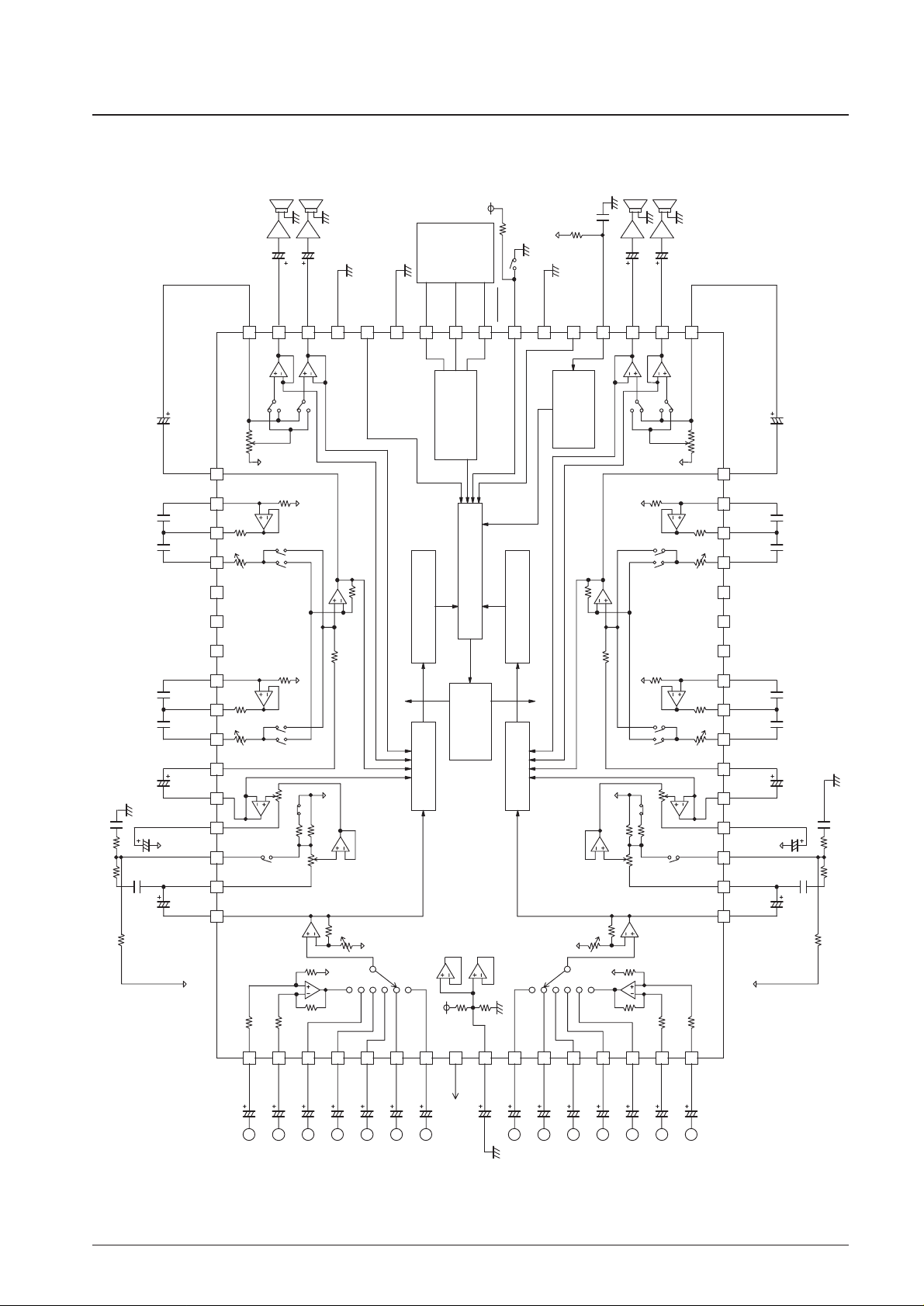
Equivalent Circuit and Sample Application Circuit Diagram
DI
VDD
VDD
CE
CL
0.033
µ
F
1 M
Ω
47 k
Ω
10
µ
F
10
µ
F
PA
L5P
L5M
L4
LFIN
µ
COM
RFIN
RFOUT
RROUT
TIM
RZCLP
RAVSS
MUTE
CE
DI
CL
LZCLP
LAVSS
LROUT
LFOUT
31
35 34 33
32
LOGIC CIRCUIT
ZERO CROSS DET
Multiplexer
ZERO CROSS DET
CCB
INTERFACE
30
29
28
27
26
25
24
23
22
21
20
19
18
17
PA
DVSS
10
µ
F
PA
10
µ
F
PA
36373839404142434445464748
14 15 1613121110987654321
504951
52
53
54
55
56
57
58
59
60
61
62
63
64
L3
L2
L1
VDD
Vref
R1
R2
R3
1
µ
×
6
R4
R5M
R5P
[BASS fo=100Hz] [TREBLE fo=10000Hz]
1 µF
0.033
µ
F
0.01
µ
F
330p F
10
µ
F
LF3C1
LF3C2
LF3C3
LTOUT
LF1C2
NC
NC
NC
NC
NC
NC
LF1C3
LF1C1
LVROUT
LTIN
LVref
Vref
LVref
LCOM
LSELO
LVRIN
LCT
10 µF
220pF
1
µ
F
0.1
µ
F68 k
Ω
4.7 k
Ω
10 µF
CONTROL
CIRCUIT
NO SIGNAL
TIMER
Multiplexer
[BASS fo=100Hz] [TREBLE fo=10000Hz]
1 µF
0.033
µ
F
0.01
µ
F
330pF
10
µ
F
RF3C1
RF3C2
RF3C3
RTOUT
RF1C2
RF1C3
RF1C1
RVROUT
RTIN
Vref
Vref
RVref
RVref
RCOM
RSELO
RVRIN
RCT
10 µF
RVref
220p F
1
µ
F
0.1
µ
F68 k
Ω
4.7 k
Ω
10 µF
22
µ
F
LVref
LVref
RVrefLVref
LVref
RVref RVref
R6
L6
1 M
Ω
• In the LC75386NW version, LZCLP (pin 28) and RZCLP (pin 21) are unused, and must be left open.
Vref
1 M
Ω
Page 6
No.6170-6/24
LC75386NE-R, 75386NW
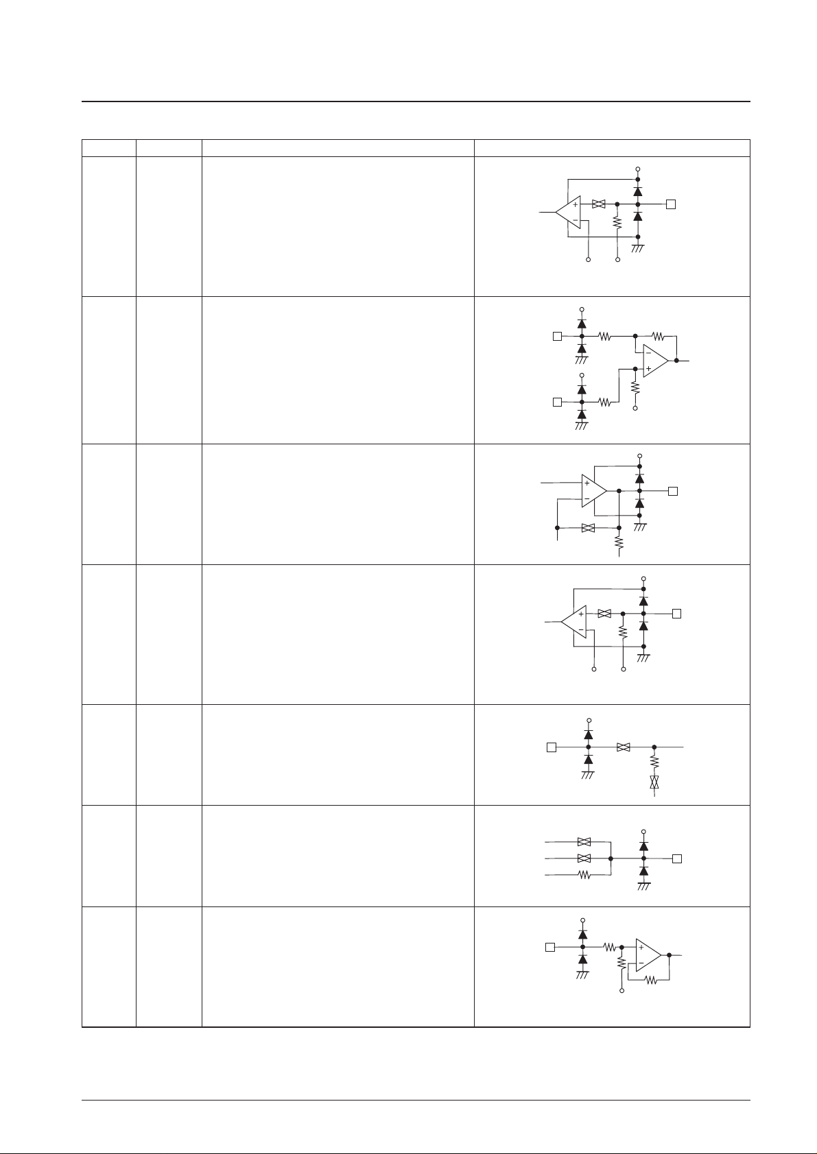
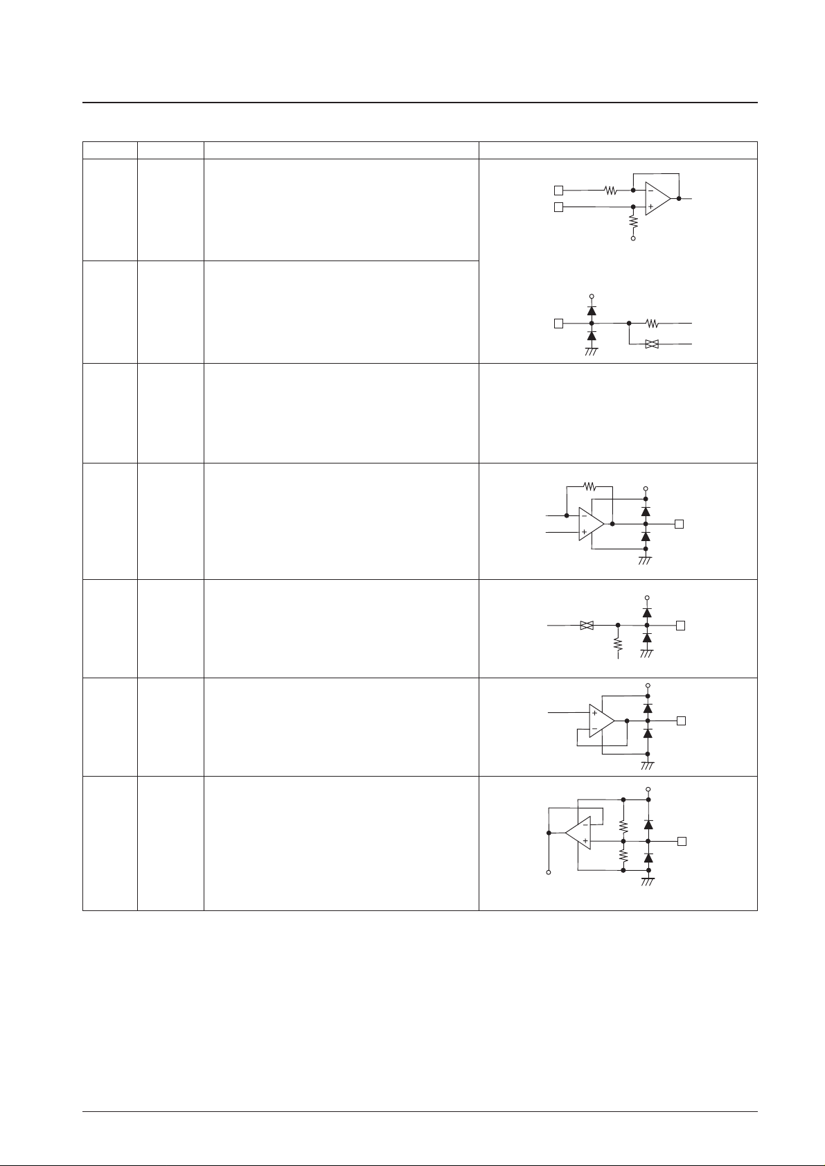
Pin Functions
Pin No. Pin Function Notes
• Single end inputs
54
53
52
51
55
59
60
61
62
58
L1
L2
L3
L4
L6
R1
R2
R3
R4
R6
V
DD
LVref
RVref
• Input selector outputs
48
1
LSEL0
RSEL0
V
DD
• Differential inputs
50
49
63
64
L5M
L5P
R5M
R5P
V
DD
M
V
DD
P
LVref
RVref
• Inputs for the 2-dB step volume control
• These inputs must be driven from low-impedance circuits.
47
2
LVRIN
RVRIN
V
DD
LVref
RVref
• Loudness function pins. Connect the high-band
compensation RC circuits between the LCT (RCT) and the
LVRIN (RVRIN) pins and connect the low-band
compensation RC circuits between the LCT (RCT) and Vref.
46
3
LCT
RCT
V
DD
• 2-dB step volume control outputs
• To reduce switching noise, each of these pins should be
connected to Vref through a capacitor.
45
4
LCOM
RCOM
V
DD
• Equalizer input
43
6
LTIN
RTIN
Continued on next page.
V
DD
LVref
RVref
Page 7
No.6170-7/24
LC75386NE-R, 75386NW
Continued from preceding page.
Pin No. Pin Function Equivalent circuit
• Equalizer input
33
16
LTOUT
RTOUT
V
DD
• Fader block inputs
• These inputs must be driven from low-impedance circuits.
32
17
LFIN
RFIN
V
DD
• Fader block outputs. The front and rear outputs can be
attenuated independently. The attenuation is the same in
the left and right channels.
31
30
18
19
LFOUT
LROUT
RFOUT
RROUT
V
DD
• Connections for the capacitors that for the tone control
circuit attenuation filter.
The low band compensation capacitors must be connected
between the following pins:
LF1C1 (RF1C1) and LF1C2 (RF1C2)
LF1C2 (RF1C2) and LF1C3 (RF1C3)
42
41
40
7
8
9
LF1C1
LF1C2
LF1C3
RF1C1
RF1C2
RF1C3
• Connections for the capacitors that for the tone control
circuit attenuation filter.
The low band compensation capacitors must be connected
between the following pins:
LF3C1 (RF3C1) and LF3C2 (RF3C2)
LF3C2 (RF3C2) and LF3C3 (RF3C3)
36
35
34
13
14
15
LF3C1
LF3C2
LF3C3
RF3C1
RF3C2
RF3C3
Continued on next page.
• Unused pins. These pins are not connected to the chip.
39
38
37
10
11
12
NC
NC
NC
NC
NC
NC
• VDD/2 voltage generator block. A capacitor with a value of
about 10 µF must be inserted between Vref and AV
SS(VSS
)
to reduce power supply ripple.
57 Vref
V
DD
LVref
RVref
C2
C3
C1
V
DD
LVref
RVref
Page 8

No.6170-8/24
LC75386NE-R, 75386NW
Continued from preceding page.
Pin No. Pin Function Equivalent circuit
• Serial data and clock inputs used for device control
26
25
CL
DI
V
DD
V
DD
• Used for the zero cross circuit no-signal timer function.
If a zero cross signal does not occur between the point
when data is loaded and the point when the timer times out,
the data will be stored forcibly when the timer times out.
20 TIM
V
DD
LVref
RVref
• Band limiting for the zero cross detection circuit
• These pins are normally left open.
• These pins are unused in the LC75386NW version and
must be left open.
28
21
LZCLP
RZCLP
24 CE
• Chip enable input. Data is written to the internal latch when
this pin goes from high to low. The analog switches then
operate.
Data transfers are enabled when this pin is high.
44
5
LVROUT
RVROUT
• 1-dB step volume control output
• Power supply56
V
DD
• Logic system ground27
DV
SS
• Analog system ground
29
22
LAV
SS
RAV
SS
V
DD
• External muting control
• When this pin is set to the V
SS
level, the fader volume block
is forcibly set to – ∞.
23 MUTE
LC75386NE-R only
V
DD
Page 9

No.6170-9/24
LC75386NE-R, 75386NW
1.25 dB
2.50 dB
3.75 dB
5.00 dB
6.25 dB
7.50 dB
8.75 dB
L5P
L5M
LSELO
0 dB
R3=22.65 k
R4=25 k
R2=25 k
R1=22.65 k
50 k
50 k
50 k
50 k
LVref
LVref
LVref
6.702 k
5.804 k
5.026 k
4.532 k
3.769 k
3.264 k
2.826 k
2.447 k
2.119 k
1.835 k
1.589 k
1.376 k
1.192 k
1.032 k
0.894 k
5.774 k
LVref
10.0 dB
11.25 dB
12.5 dB
13.75 dB
15.0 dB
16.25 dB
17.5 dB
18.75 dB
L4
L3
LVref
LVref
IN MUTE SW
LVref
L2
L1
50 k
LVref
L6
Internal Equivalent Circuits
Selector Block Equivalent Circuit
Total resistance: 50 kΩ
The right channel is identical.
Unit (Resistance: Ω)
Page 10

No.6170-10/24
LC75386NE-R, 75386NW
To the left
channel 1-dB
step block
LVref
41.139 k
32.678 k
25.957 k
20.618 k
16.378 k
-2dB
-4dB
-6dB
-8dB
-10dB
-12dB
-14dB
0dB
-16dB
-18dB
-20dB
-22dB
-24dB
-26dB
-28dB
-30dB
-32dB
-34dB
-36dB
-38dB
-40dB
-42dB
-44dB
-46dB
-48dB
-50dB
-52dB
-54dB
-56dB
-58dB
-60dB
-62dB
-64dB
-66dB
-68dB
-70dB
-72dB
-74dB
-76dB
-78dB
-∞ dB
13.009 k
10.334 k
8.208 k
6.520 k
5.179 k
4.114 k
3.268 k
2.596 k
2.062 k
1.638 k
1.301 k
6.344 k
5.040 k
LCT
5.750 k
4.003 k
3.180 k
2.526 k
2.006 k
1.594 k
1.266 k
1.006 k
0.799 k
0.634 k
0.504 k
0.400 k
0.318 k
0.253 k
0.201 k
0.159 k
0.127 k
0.101 k
0.080 k
0.063 k
0.050 k
0.040 k
0.154 k
LVRIN
2-dB Step Volume Control Block Equivalent Circuit
• The total resistance above the
tap is 195 kΩ
• The total resistance below
the tap is 30.847 kΩ
The right channel is identical.
Unit (Resistance: Ω)
Page 11

No.6170-11/24
LC75386NE-R, 75386NW
1-dB Step Volume Control Block Equivalent Circuit
5.438 k
44.564 k
LVROUT
Vref
-1 dB
-∞ dB
LCOM
0 dB
Unit: (Resistance : Ω)
Total resistance: 50 kΩ
The right channel is identical.
Tone Control Block Equivalent Circuit
LTOUT
50 k
LTIN
5.1 k
LVref
5.1 k
0.711 k
0.648 k
12 dB
1.015 k
1.751 k
3.595 k
10.977 k
10 dB
8 dB
6 dB
4 dB
LF1C1 LF1C2 LF1C3
68 k
1 k
LVref
LVref
LVref
LVref
0.711 k
0.648 k
12 dB
1.015 k
1.751 k
3.595 k
10.977 k
10 dB
8 dB
6 dB
4 dB
LF3C1 LF3C2 LF3C3
68 k
1 k
From the left channel
2-dB volume control
block
Switch used for initial setup
Switch used for initial setup
Unit: (Resistance : Ω)
Page 12

No.6170-12/24
LC75386NE-R, 75386NW
Fader Volume Control Block Equivalent Circuit
LFIN
5.437 k
4.846 k
8.169 k
4.094 k
LFOUT
LVref
-1 dB
-2 dB
0 dB
S1
S2
S3
S4
6.489 k
5.154 k
-6 dB
-8 dB
-4 dB
3.252 k
2.583 k
2.052 k
3.419 k
-12 dB
-14 dB
-10 dB
1.630 k
1.295 k
-18 dB
-20 dB
-16 dB
1.300 k
0.231 k
-45 dB
-60 dB
-∞ dB
-30 dB
0.050 k
LROUT
When FADER is set to 1, S2 and S3 will be turned on.
When FADER is set to 0, S1 and S4 will be turned on.
Unit: (Resistance : Ω)
Total resistance: 50 kΩ
If data that sets the main volume control 1-dB step circuit to –∞ is sent to the device, switches S1
and S2 will be opened (off) and switches S3 and S4 will be closed (on).
Page 13

Control System Timing and Data Format
The LC75386NE-R/NW are controlled by applying the stipulated data to the CL, DI, and CE pins. The data consists of a
total of 52 bits, of which 8 bits are the device address and 44 bits are the actual control data.
• Address code (B0 to A3)
The LC75386NE-R/NW have an 8-bit address codes, and can be used along with other ICs that support the Sanyo CCB
serial bus.
No.6170-13/24
LC75386NE-R, 75386NW
CE
DI
D43D42D41D40D39D38D5D4D3D2D0 D1A3A2A1A0B3B2B1B0
CL
minmin
≤ T
DEST
1 µs
1 µs
1 µs
1 µs1 µs1 µs
min
min
min
CE
DI
CL
Address code
B0 B1 B2 B3 A0 A1 A2 A3
10000001
(LSB)
(81HEX)
• Control code allocation
D0 D1 D2 Setting
0 0 0 L1 (R1)
1 0 0 L2 (R2)
0 1 0 L3 (R3)
1 1 0 L4 (R4)
0 0 1 L5 (R5)
1 0 1 L6 (R6)
011
111
Input switching control
IC test values. These values must not
be used during normal operation.
D3 IC test bit. This bit must be set to 0 during normal operation.
Page 14

No.6170-14/24
LC75386NE-R, 75386NW
D4 D5 D6 D7 Operation
0 0 0 0 0 dB
1 0 0 0 +1.25 dB
0 1 0 0 +2.50 dB
1 1 0 0 +3.75 dB
0 0 1 0 +5.00 dB
1 0 1 0 +6.25 dB
0 1 1 0 +7.50 dB
1 1 1 0 +8.75 dB
0 0 0 1 +10.0 dB
1 0 0 1 +11.25 dB
0 1 0 1 +12.5 dB
1 1 0 1 +13.75 dB
0 0 1 1 +15.0 dB
1 0 1 1 +16.25 dB
0 1 1 1 +17.5 dB
1 1 1 1 +18.75 dB
Input gain control
Page 15

No.6170-15/24
LC75386NE-R, 75386NW
D8 D9 D10 D11 D12 D13 D14 D15 Operation
1-dB step
0 0 dB
1 –1 dB
2-dB step
0 0 0 0 0 0 0 0 dB
1 0 0 0 0 0 0 –2 dB
0 1 0 0 0 0 0 –4 dB
1 1 0 0 0 0 0 –6 dB
0 0 1 0 0 0 0 –8 dB
1 0 1 0 0 0 0 –10 dB
0 1 1 0 0 0 0 –12 dB
1 1 1 0 0 0 0 –14 dB
0 0 0 1 0 0 0 –16 dB
1 0 0 1 0 0 0 –18 dB
0 1 0 1 0 0 0 –20 dB
1 1 0 1 0 0 0 –22 dB
0 0 1 1 0 0 0 –24 dB
1 0 1 1 0 0 0 –26 dB
0 1 1 1 0 0 0 –28 dB
1 1 1 1 0 0 0 –30 dB
0 0 0 0 1 0 0 –32 dB
1 0 0 0 1 0 0 –34 dB
0 1 0 0 1 0 0 –36 dB
1 1 0 0 1 0 0 –38 dB
0 0 1 0 1 0 0 –40 dB
1 0 1 0 1 0 0 –42 dB
0 1 1 0 1 0 0 –44 dB
1 1 1 0 1 0 0 –46 dB
0 0 0 1 1 0 0 –48 dB
1 0 0 1 1 0 0 –50 dB
0 1 0 1 1 0 0 –52 dB
1 1 0 1 1 0 0 –54 dB
0 0 1 1 1 0 0 –56 dB
1 0 1 1 1 0 0 –58 dB
0 1 1 1 1 0 0 –60 dB
1 1 1 1 1 0 0 –62 dB
0 0 0 0 0 1 0 –64 dB
1 0 0 0 0 1 0 –66 dB
0 1 0 0 0 1 0 –68 dB
1 1 0 0 0 1 0 –70 dB
0 0 1 0 0 1 0 –72 dB
1 0 1 0 0 1 0 –74 dB
0 1 1 0 0 1 0 –76 dB
1 1 1 0 0 1 0 –78 dB
Mute
11111 10–∞
Volume Control
Page 16

No.6170-16/24
LC75386NE-R, 75386NW
D16 D17 D18 D19 Bass
D24 D25 D26 D27 Treble
0 1 1 0 +12 dB
1 0 1 0 +10 dB
0 0 1 0 +8 dB
1 1 0 0 +6 dB
0 1 0 0 +4 dB
1 0 0 0 +2 dB
0 0 0 0 0 dB
1 0 0 1 –2 dB
0 1 0 1 –4 dB
1 1 0 1 –6 dB
0 0 1 1 –8 dB
1 0 1 1 –10 dB
0 1 1 1 –12 dB
D20 D21 D22 D23 Setting
0 0 0 0 Must be set to 0.
Tone control
Fader Volume Control
D28 D29 D30 D31 Operation
0 0 0 0 0 dB
1 0 0 0 –1 dB
0 1 0 0 –2 dB
1 1 0 0 –4 dB
0 0 1 0 –6 dB
1 0 1 0 –8 dB
0 1 1 0 –10 dB
1 1 1 0 –12 dB
0 0 0 1 –14 dB
1 0 0 1 –16 dB
0 1 0 1 –18 dB
1 1 0 1 –20 dB
0 0 1 1 –30 dB
1 0 1 1 –45 dB
0 1 1 1 –60 dB
1111 –∞
Channel Selection Control
D32 D33 Setting
0 0 Left and right together. This is the mode set up initially
1 0 RCH
0 1 LCH
1 1 Left and right together
Fader Rear/Front Control
D34 Setting
0 Rear
1 Front
Page 17

No.6170-17/24
LC75386NE-R, 75386NW
Loudness Control
D35 Setting
0 Off
1On
Zero Cross Control
D36 D37 Setting
0 0 Data is written when a zero cross is detected
1 1 The zero cross detection operation is disabled and data is written on the falling edge of the CE signal
D38 D39 D40 D41 Setting
0 0 0 0 Selector
1 0 0 0 Volume
0 1 0 0 Tone
1 1 0 0 Fader
Zero Cross Signal Detection Block Control
Test Mode Control
D42 D43 Setting
0 0 These IC test mode control bits must be set to 0
Page 18

Usage Notes
Data Transmission after Power Is First Applied
• When power is first applied, the state of the internal analog switches will be undefined. Applications that use this IC
must include external circuits to provide muting until control data has been transferred to the IC.
• After power is first applied, applications should send initial setup data to stabilize the bias levels in each of the IC
circuit blocks in a short time.
1. The time between initial setup mode and the first actual data settings
• Applications should send the initial setup data as soon as VDDrises above 6 V.
• After the LCOM and RCOM pins have stabilized at the Vref level, applications should send the first data settings.
2. Procedure for setting up initial setup mode
• When D32 and D33 are set to 00, the IC’s internal initial setup switch is turned on and the IC goes to quick charge
mode. At this time the other data (D0 to D31 and D34 to D43) will also be set up for the left and right channels at the
same time. This means that applications can set up the states of the various blocks at the same time as specifying initial
setup mode.
3. Procedure for clearing initial setup mode
• Initial setup mode is cleared by setting D32 and D33 to any value other than 00. In other words, any normal left or
right channel specification will turn the internal initial setup switch off and clear quick charge mode.
No.6170-18/24
LC75386NE-R, 75386NW
The time required for the capacitors connected to the LCOM
and RCOM pins to be charged to the Vref level
VREF
V
DD
These operations
clear initial setup
mode
The 1/2 VDDlevel
VDD= 9 V (TYP)
VDD= 6 V
Initial setup
mode
First data for
the left channel
First data for
the right
channel
Data
Page 19

Zero Cross Switching Circuit Operating Principles
• The LC75386NE-R/NW include functions for switching the place where the zero cross comparator operates and thus
allows applications to select the optimal detection location for the block for which the control data is updated.
Basically, switching noise will be minimized if the signal immediately following the block for which the control data is
updated is input to the zero cross comparator. Thus the detection location must be changed for each data update
operation. Another issue is the point that if the signal amplitude is lower than the detection sensitivity (a few mV rms)
of the zero cross comparator (for example if the volume is set to a low level), the switching noise can be minimized
further by selecting a point before the volume control block, namely the selector block output, as the zero cross
detection point than by simply waiting for the data write to occur due to the overflow of the zero cross timer. For
example, if the volume block input is 1 V rms, and the volume is set to –40 dB or lower, the output will be under
10 mV rms. In this case, detecting at the selector output block will result in lower switching noise.
No.6170-19/24
LC75386NE-R, 75386NW
Zero Cross Switching Control Procedure
• The zero cross switching control procedure consists of first setting the zero cross detection mode with the zero cross
control bits (D36 and D37 = 0) and then, after specifying the detection block (with bits D38, D39, D40, and D41),
sending the control data. Since these control bits are latched first immediately after the data is sent, i.e. on the falling
edge of the CE signal, it is possible to both set the IC mode as well as specify zero cross switching operation in a single
data transfer, even when updating the volume and other data. The following presents an example of the control
operation when updating the volume block data.
D36
Zero cross detection
mode specification
Volume block setting
D37 D38 D39 D40 D41
001000
Zero Cross Timer Setting
• When the input signal has a level lower than the sensitivity of the zero cross comparator, or consists only of extremely
low frequencies, the zero cross detection circuit will remain in the state in which it cannot detect a zero cross and the
data will not be latched during that period. The zero cross timer specifies a time after which the data will be latched
forcibly in states where a zero crossing cannot be detected. The time is determined by the lowest frequency for which a
zero cross can be detected reliably.
For example, if the timer is set to 25 ms:
T = 0.69 CR
If C is taken to be 0.033 µF, then R will be:
R =
25 × 10
-3
≈ 1.1 MΩ
0.69 × 0.033 × 10
-6
Selector
Volume Tone
Fader
Switch
Zero cross
comparator
Zero Cross Detection Circuit
Page 20

Notes on Serial Data Transfer
1. The CL, DI, and CE pin signal lines must be covered (and thus shielded) by the ground pattern or formed from
shielded cable to prevent the high-frequency digital signals on those lines from entering the analog system.
2. The LC75386NE-R/NW data formats consist of 8 bits of address and 44 bits of data. When the data is sent in units of
8 bits each (i.e. 48 bits are actually sent), use the data transfer technique shown in figure 1.
LC75386NE-R/NW data receptions in 8-bit units
No.6170-20/24
LC75386NE-R, 75386NW
Dummy data
3. During CCB transfers, this IC detects address matches on the rising edge of the CE signal. Therefore, applications
must set the CL signal low and then set it high at this time.
D36
.......
Input switching control
Test mode control
X: don't care
D43D42D41D40D39D38D37
D3D2D1D0XXXX
Page 21

No.6170-21/24
LC75386NE-R, 75386NW
0
-
2
-
4
-
6
-
8
-
10
-
12
-
14
-
16
-
18
-
20
-
22
-
24
-
26
-
28
-
30
-
32
-
34
-
36
-
38
-
40
-
42
-
44
-
46
-
48
-
50
-
52
-
54
-
60
10
23 57 23 57 23 57 23 57
100 1k 10k 100k
-
50
-
40
-
30
-
20
-
10
0
10
20
Loudness Characteristics
Level — dB
Frequency, f — Hz
0
-
2
-
4
-
6
-
8
-
10
-
12
-
14
-
16
-
18
-
20
-
22
-
24
-
26
-
28
-
30
-
32
-
34
-
36
-
38
-
40
-
42
-
44
-
46
-
48
-
50
-
52
-
54
0
-
60
10
23 57 23 57 23 57 23 57
100 1k 10k 100k
-
50
-
40
-
30
-
20
-
10
10
20
Output Level Characteristics
VDD= 9 V, VSS= 0 V, VIN= 0 dBV
Flat overall
Input = L1, Output = LFOUT
Settings: the 0 dB to –54 dB positions (in –2 dB steps)
VDD= 9 V, VSS= 0 V, VIN= 0 dBV
Flat overall
Input = L1, Output = LFOUT
Settings: the 0 dB to –54 dB positions (in –2 dB steps)
Output level — dBV
Frequency, f — Hz
Page 22

No.6170-22/24
LC75386NE-R, 75386NW
-∞
-
70-60-50-40-30-20-10 0
-
80
-
70
-
60
-
50
-
40
-
30
-
10
-
20
0
-∞
-
70-60-50-40-30-20-10 0
-
90
-
80
-
70
-
60
-
50
-
40
-
30
-
10
-
20
0
042 6 8 101214161820
0
2
4
6
8
10
12
18
14
16
20
10
23 57 23 57 23 57 23 57
100 1k 10k 100k
0.01
0.1
1.0
7
5
3
2
7
5
3
2
7
5
3
2
0.001
V V
V
THD
METER
Fader block
Main Volume Step Characteristics
Attenuation — dB
Step — dB
Input gain block
Main volume block
Graphic equalizer block
Gain Step Characteristics
Step — dB
Output level — dB
Fader Volume Step Characteristics
Step — dB
Fader volume attenuation — dB
THD – Frequency Characteristics
Total harmonic distortion, THD — %
Frequency, f — Hz
Fader block
Input gain block
Main volume block
Graphic equalizer block
Fader block
Input gain block
Main volume block
Graphic equalizer block
Fader block
Input gain block
Main volume block
Graphic equalizer block
VDD= 9 V, VSS= 0 V, VIN= –10 dBV
Input = L1, Output = LFOUT
80-kHz low pass weighting
VDD= 9 V
VSS= 0 V
VIN= 0 dBV
f = 1 kHz
VDD= 9 V
VSS= 0 V
VIN= –20 dBV
f = 1 kHz
VDD= 9 V
VSS= 0 V
VIN= 0 dBV
f = 1 kHz
Page 23

No.6170-23/24
LC75386NE-R, 75386NW
3
2
5
7
3
2
5
7
3
2
5
7
3
2
5
7
3
2
5
7
3
2
5
7
f = 1kHz
f = 20kHz
V
IN
= 0dBV, f = 20kHz
V
IN
= 0dBV, f = 1kHz
V
IN
= -10dBV, f = 20kHz
V
IN
= -10dBV, f = 1kHz
10 100
7532753275327532
1k 10k 100k
-
40
-
35
-
30
-
25
-
20
-
15
-
10
-
5
10 100
7532753275327532
1k 10k 100k
-
40
-
35
-
30
-
25
-
20
-
15
-
10
-
5
0
0
0.001
0.01
0.1
1.0
-20-40 -35 -30 -25 -15 -10 -5 0 5 10
0.001
0.01
0.1
1.0
84567 910111213
THD
METER
THD
METER
Frequency — Hz
Level — dB
Bass Characteristics
V
DD
= 9 V,V
SS
= 0 V,V
IN
= –20 dBV
Input = L1, Output = LF OUT
V
DD
= 9 V,V
SS
= 0 V,V
IN
= –20 dBV
Input = L1, Output = LF OUT
Frequency — Hz
Level — dB
Treble Characteristics
Fader block
THD – Input Level Characteristics
Input gain block
Main volume block
Graphic equalizer block
THD – Supply Voltage Characteristics
Supply voltage — V
Total harmonic distortion, THD — %
Fader block
Input gain block
Main volume block
Graphic equalizer block
Total harmonic distortion, THD — %
Input level, VIN— dBV
VDD= 9 V, VSS= 0 V
80-kHz low pass weighting
With VRset to the 0 dB position
VSS= 0 V
80-kHz low pass weighting
Page 24

This catalog provides information as of March, 2000. Specifications and information herein are subject to
change without notice.
Specifications of any and all SANYO products described or contained herein stipulate the performance,
characteristics, and functions of the described products in the independent state, and are not guarantees
of the performance, characteristics, and functions of the described products as mounted in the customer’s
products or equipment. To verify symptoms and states that cannot be evaluated in an independent device,
the customer should always evaluate and test devices mounted in the customer’s products or equipment.
SANYO Electric Co., Ltd. strives to supply high-quality high-reliability products. However, any and all
semiconductor products fail with some probability. It is possible that these probabilistic failures could
give rise to accidents or events that could endanger human lives, that could give rise to smoke or fire,
or that could cause damage to other property. When designing equipment, adopt safety measures so
that these kinds of accidents or events cannot occur. Such measures include but are not limited to protective
circuits and error prevention circuits for safe design, redundant design, and structural design.
In the event that any or all SANYO products (including technical data, services) described or contained
herein are controlled under any of applicable local export control laws and regulations, such products must
not be exported without obtaining the export license from the authorities concerned in accordance with the
above law.
No part of this publication may be reproduced or transmitted in any form or by any means, electronic or
mechanical, including photocopying and recording, or any information storage or retrieval system,
or otherwise, without the prior written permission of SANYO Electric Co., Ltd.
Any and all information described or contained herein are subject to change without notice due to
product/technology improvement, etc. When designing equipment, refer to the “Delivery Specification”
for the SANYO product that you intend to use.
Information (including circuit diagrams and circuit parameters) herein is for example only; it is not
guaranteed for volume production. SANYO believes information herein is accurate and reliable, but
no guarantees are made or implied regarding its use or any infringements of intellectual property rights
or other rights of third parties.
PS No.6170-24/24
LC75386NE-R, 75386NW
 Loading...