

SANYO LC7537NE, LC7537AN, LC7537 Datasheet
CMOS LSI
Ordering number : EN2169C
81096HA(OT)/31293JN/7018YT/6186KI,TS No. 2169-1/11
SANYO Electric Co.,Ltd. Semiconductor Bussiness Headquarters
TOKYO OFFICE Tokyo Bldg., 1-10, 1 Chome, Ueno, Taito-ku, TOKYO, 110 JAPAN
Electronic Volume Control System for
Audio Equipment
LC7537, 7537AN, 7537NE
Overview
The LC7537N is an electronic control LSI capable of
electronically controlling the volume, balance, loudness,
fader, bass, and treble functions individually with fewer
externally connected component parts.
Features
• Enables controlling the below-listed functions with 3line serial data, including CE, DI, and CLK. Also, due
to 0 V to 5 V swing of the serial data input voltage,
permits the use of a general purpose microcomputer.
Volume : Separately controls the Lch and Rch
volume levels across 81 positions over
the 0 dB to –79 dB (in 1 dB steps) range
and –∞, and consequently also serves
balance control purposes.
Loudness : By virtue of a center tap provided at the
–20 dB position of the volume
controlling ladder resistors, permits
loudness to be controlled with
externally connected CR components.
Fader : By varying only the rear or front output
level across 16 positions, provides fader
functions (in 2 dB steps over the 0 dB to
–20 dB range, and 5 dB steps over the
–20 dB to –45 dB range, and at –∞, for
a total of 16 positions).
Bass/Treble : With CR components externally
connected, forms an NF type tone
control circuit (Baxandall type) to
exercise control across 15 positions
over both the bass and treble functions
in 2 dB steps.
• By virtue of its CMOS structure, the LSI operates under
a broad power supply voltage range from +4.5 V to +15
V, permitting the use of either a single or a dual ± power
supply, whichever is preferred.
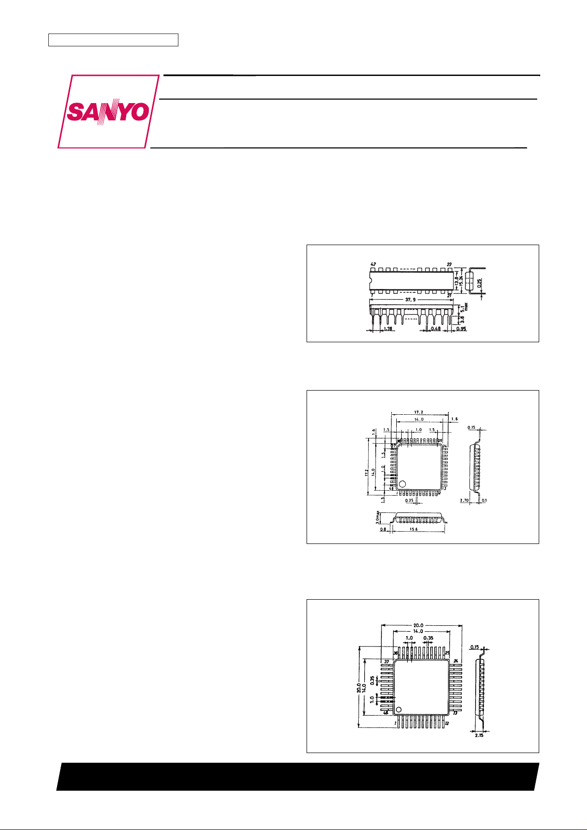
Package Dimensions
SANYO: DIP42S
[LC7573N]
unit : mm
3025B-DIP42S
SANYO: QIP48E
[LC7537NE]
SANYO: QIP48A
[LC7537AN]
unit : mm
3156-QFP48E
unit : mm
3052A-QFP48A
Absolute Maximum Ratings at Ta = 25°C, VSS= 0 V, VDD= ≥ VCC> VSS≥ V
EE
No. 2169-2/11
LC7537N, 7537AN, 7537NE
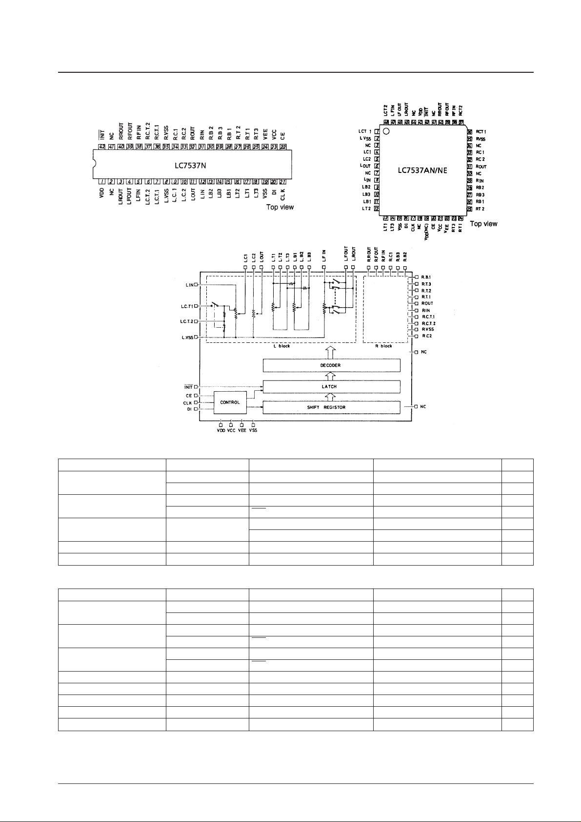
Pin Assignments
Equivalent Circuit Block Diagram
Specifications
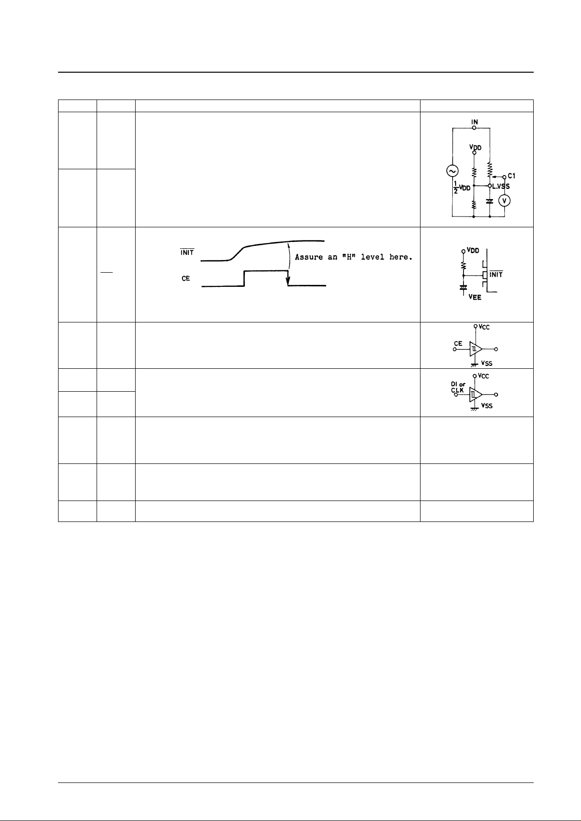
Note: 1. A1000 pF or larger capacitor should be added on between each individual power supply terminal and VSS.
2. When the microcomputer side control signals rise faster than V
DD
for the LC7537, a 2 kΩ or higher resistor should be inserted midway on each of
the DI, CLK, and CE lines.
3. When mounting the QIP package on the board, do not dip the entire package in solder. Only the LC7537NE may be dipped directly in solder during
mounting.
Item Symbol Condition Rating Unit
Maximum supply voltage
V
DD
– VEEmax VDD, VEE: VEE≥ –8 V 16 V
V
CC
max VCC: VDD≥ V
CC
V
SS
– 0.3 to V
SS
+ 7 V
Input supply voltage
V
I1
DI, CLK, CE V
SS
– 0.3 to V
DD
+ 0.3 V
V
I2
INIT V
SS
– 0.3 to V
DD
+ 0.3 V
Allowable power dissipation Pd max
Ta ≤ 85˚C, (LC7537N, 7537AN) 200 mW
Ta ≤ 85˚C, (LC7537NE) 300 mW
Operating temperature Topr –40 to +85 ˚C
Storage temperature Tstg *3 –50 to +125 ˚C
Allowable Operating Conditions at Ta = 25°C, VSS= 0 V, VDD= ≥ VCC> VSS≥ V
EE
Item Symbol Condition Rating Unit
Supply voltage *1
V
DD
– V
EE
VEE≥ –7.5 V 4.5 to 15 V
V
CC
4.5 to 5.5 V
Input high–level voltage
V
IH1
*2 DI, CLK, CE 0.8 VCCto V
CC
V
V
IH2
INIT 0.8 (V
DD
– VEE) + VEEto V
DD
V
Input low–level voltage
V
IL1
*2 DI, CLK, CE VSSto 0.2 V
CC
V
V
IL2
INIT VEEto 0.2 (V
DD
– VEE) + V
EE
V
Input signal amplitude V
IN
VEEto V
DD
V
P-P
Input pulse width tø
W
1 min µs
setup time t
set up
1 min µs
Hold time t
hold
1 min µs
Operating frequency f
opg
up to 330 kHz

No. 5190-3/10
LC7537N, 7537AN, 7537NE
Item Symbol Condition
Rating
min typ max Unit
Total harmonic THD(1) V
IN
= 1 V, f = 1kHz, all flat overall 0.005 0.01 %
Distortion THD(2) V
IN
= 1 V, f = 20 kHZ, all flat overall 0.006 0.02 %
Crosstalk
CT V
IN
= 1 V, f = 1 kHz, all flat, Rg = 1 kΩ 60 95 dB
V
omin
(1) VIN= 1 V, f = 1 kHz, MAIN, VR = ∞, FADER VR = ∞ 80 90 dB
Maximum attenuation output
V
omin
(2) VIN= 1 V, f = 1 kHz, MAIN, VR = ∞, VDD= 8 V, FADER VR = ∞,
70 80 dB
V
EE
= VSS= 0 V, C between VSSand GND of L/R = 1000 µF
R
VOL
(1) 5 dB-step 12 20 28 kΩ
R
VOL
(2) 1 dB-step 12 20 28 kΩ
VR resistance voltage R
BASS
12 20 28 kΩ
R
TREBLE
12 20 28 kΩ
R
FADER
12 20 28 kΩ
Output noise
V
N
(1) All flat overall (I
HF-A
) Rg = 1 kΩ 2 10 µV
V
N
(2) Rg = 1 kΩ, VDD= 8 V, VEE= VSS= 0 V 2 10 µV
Current drain
I
DD
V
DD
– VEE= 15 V 1 mA
I
CC
VCC= 5 V 1 mA
Continued on next page.
Electrical Characteristics at Ta = 25°C, VDD=+7.5 V, VEE=–7.5 V, VCC=+5 V
Pin No. Symbol Description of Functions Remarks
12(8) L.IN
31(29) R.IN
9(4) L.C1
34(33) R.C1
10(5) L.C2
33(32) R.C2
11(6) L.OUT
32(31) R.OUT
5(47) L.FIN
38(38) R.FIN
4(46) L.FOUT
3(45) L.ROUT
39(39) R.ROUT
40(40) R.ROUT
15(11) L.B1
16(9) L.B2
14(10) L.B3
28(26) R.B1
27(28) R.B2
29(27) R.B3
17(13) L.T1
16(12) L.T2
18(14) L.T3
26(24) R.T1
27(25) R.T2
25(23) R.T3
7(1) LCT1
6(48) LCT2
36(36) RCT1
37(37) RCT2
Main volume control block 5 dB-step attenuator input terminals. These pins should be
driven at a low impedance.
Main volume control block 5 dB-step attenuator output terminals. Having been designed
to be open, the step positions will develop errors if at low acceptor impedances, so that as
high load impedances as possible should be provided.
VR resistance : 20 kΩ
VR resistance : 20 kΩ
VR resistance : 20 kΩ
Main volume control block 1 dB-step attenuator input terminals. Theses pins should be
driven at alow impedance.
Main volume control block 1 dB-step attenuator output terminals. Due to the step
positions designed to be open, load impedances as high as possible should be provided to
them, similar to those for the LC1 and RC1.
Fader functions employing mode input terminals. These pins should be driven at a low
impedance.
Fader block output terminals. These pins permit the front and rear sides to be faded out
independently of each other. Attenuations exercised on Lch will be the same as on Rch.
Due to the step positions designed to be open, acceptor impedances as high as possible
should be provided to them.
Pin Description ( ) : LC7537AN, 7537NE
Bass tone control block terminals. A total of 15 positions have been provided in 2 dB
steps
Treble tone control block terminals. A total of 15 positions have been provided in 2 dB
steps. The VR resistance value is 20 kΩ.
VR resistance : 20 kΩ
VR resistance : 20 kΩ
Loudness dedicated terminals. A high-frequency-range correcting C should be put
between CT1 and IN, and low-frequency-range correcting C between CT2 and L–V
SS
(R–VSS).
No. 2169-4/11
LC7537N, 7537AN, 7537NE
Pin No. Symbol Description of Functions Remarks
8(2) L-V
SS
35(35) R-V
SS
42(42) INIT
22(20) CE
20(16) DI
21(17) CLK
1(43) V
DD
23(21) V
CC
19(15) V
SS
24(22) V
EE
2(3, 7)
41(18, 30, NC
34, 41, 44)
(19) V
DD
(NC)
Main volume control block fader control common terminals. The impedance of pattern
connected to these pins should be as low as possible. Since L–V
SS
(R–VSS) and V
SS
have not been connected inside the LSI, they should be connected together on the outside
in conformance with their individual specifications. Particular attenuation should be paid to
the capacitance assigned to the capacitors put between L–V
SS
(R–VSS) and VSS, which
will emerge as a residual resistive component when control is turned down for maximum
attenuation.
Intra-IC latch resetting terminal
Control-setting data at the internal latch will be indeterminate when power has just been
switched on, so that by engaging the “L” level of this pin at power-on, the fader control
may be set at its –∞ position and muting behaviour is engaged (Note: V
DD
to VEELevel).
Chip enable terminal. When this pin is made “H” to “L”, data is written in the internal latch,
activating the various analog switches. When the “H” level is then restored, transfer of the
data will be enabled.
Input terminals for serial data and clock that serve control purposes.
Continued from preceding page.
These pins are connected to the relevant power supplies. Exercise caution against V
CC
rising earlier than VDD.
No connect pins. Absolutely nothing should be connected here.
LC7537AN and
LC7537NE only
V
DD
subterminal. Connected to VDDor left open.
 Loading...