SANYO LC75373E Datasheet

CMOS LSI
Ordering number : EN5588
22798HA (OT) No. 5588-1/21
SANYO Electric Co.,Ltd. Semiconductor Bussiness Headquarters
TOKYO OFFICE Tokyo Bldg., 1-10, 1 Chome, Ueno, Taito-ku, TOKYO, 110-8534 JAPAN
Electronic Volume Control
for Car Stereo Systems
LC75373E
Overview
The LC75373E is an electronic volume control that can
implement volume, balance, fader, bass/treble + super
bass, loudness, input switching, and input/output level
control functions with a minimal number of external
components.
Functions
• Volume: Provides 81 positions, from 0 dB to –79 dB (in
1-dB steps) and –∞. A balance function can be
implemented by controlling the left and right channels
independently.
• Fader: This function can attenuate either the rear or the
front outputs over 16 positions. (From 0 to –20 dB in
2-dB steps, from –20 to –25 dB in one 5-dB step, from
–25 to –45 dB in 10-dB steps, –60 dB, and –∞.)
• Bass/treble: Forms an NF-type tone control circuit with
the addition of external capacitors. The base and treble
controls each have 15 positions.
• Input gain: The input signal can be amplified from 0 dB
to +18.75 dB in 1.25 dB steps.
• Output gain: One of two output of 0 dB and + 6.5 dB
can be selected for fader output.
• Input switch: The signal can be selected from one of
four inputs for each of the left and right channels.
• Super bass: The position of super bass can be controlled
in 11 steps.
Features
• On-chip buffer amplifiers for a minimum of external
components.
• Built-in reference voltage generation circuit
• Serial data input: Supports CCB format communication
with the system controller.
Package Dimensions
unit: mm
3148-QFP44MA
SANYO: QIP44MA
[LC75373E]
• CCB is a trademark of SANYO ELECTRIC CO., LTD.
• CCB is SANYO’s original bus format and all the bus
addresses are controlled by SANYO.
Specifications
Absolute Maximum Ratings at Ta = 25°C, VSS= 0 V
Parameter Symbol Conditions Ratings Unit
Maximum supply voltage V
DD
max V
DD
11 V
Maximum input voltage V
IN
max CL, DI, CE VSS– 0.3 to VDD+ 0.3 V
Operating temperature Topr –40 to +85 °C
Storage temperature Tstg –50 to +125 °C
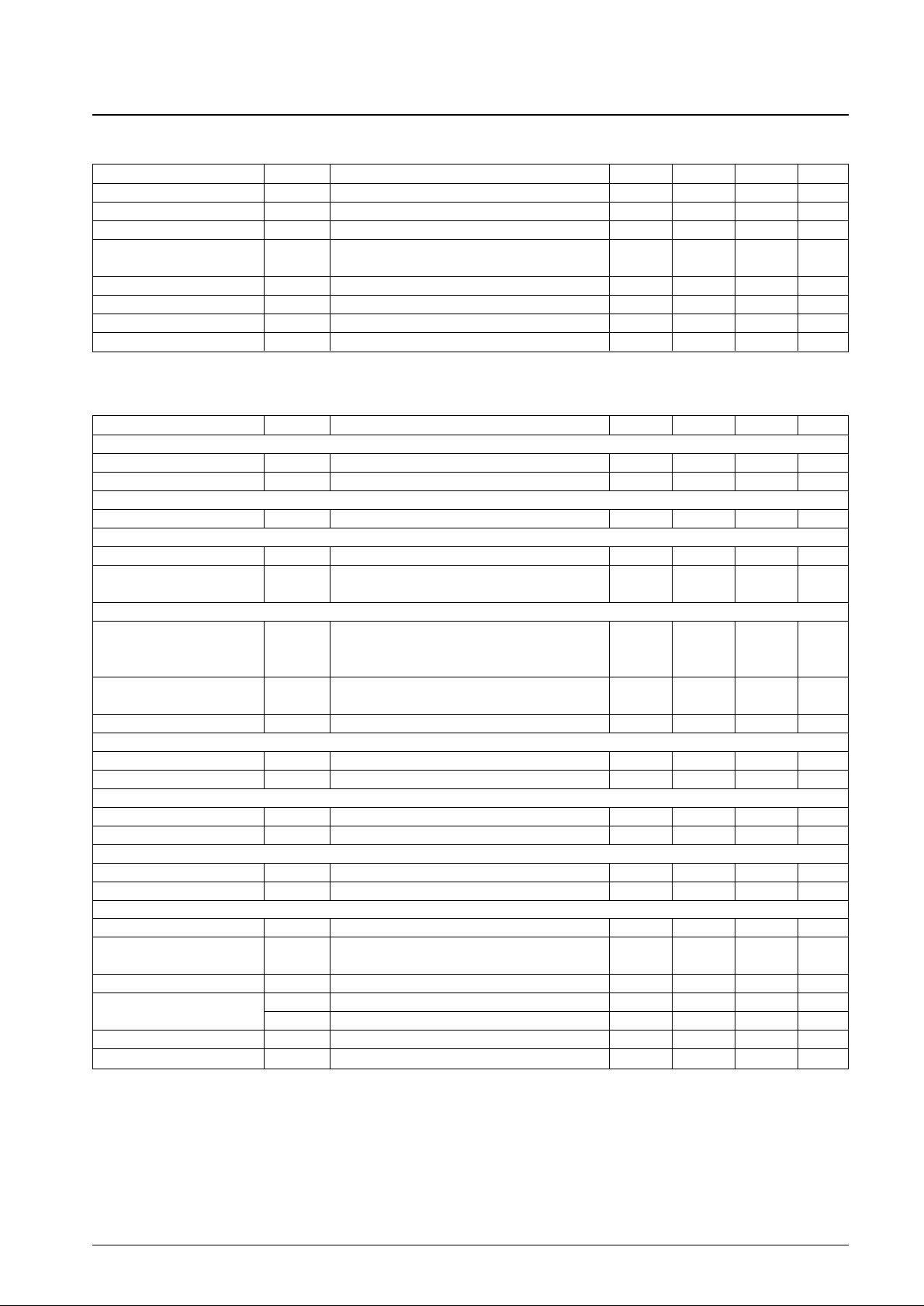
Allowable Operating Ranges at Ta = 25°C, VSS= 0 V
Electrical Characteristics at Ta = 25°C, VDD= 8 V, VSS= 0 V
Note: Values in parenthesis are targets and will be fixed after evaluation.
No. 5588-2/21
LC75373E
Parameter Symbol Conditions min typ max Unit
Supply voltage V
DD
V
DD
6.0 10.5 V
Input high-level voltage V
IH
CL, DI, CE 4.0 V
DD
V
Input low-level voltage V
IL
CL, DI, CE V
SS
1.0 V
Input voltage amplitude V
IN
CL, DI, CE, LVRIN, RVRIN, L1 to L4, R1 to R4
V
SS
V
DD
Vp-p
LFIN, RFIN, LSIN, RSIN
Input pulse width t
øW
CL 1 µs
Setup time tsetup CL, DI, CE 1 µs
Hold time thold CL, DI, CE 1 µs
Operating frequency fopg CL 500 kHz
Parameter Symbol Conditions min typ max Unit
[Input Block]
Maximum input gain Gin max +18.75 dB
Step resolution Gstep +1.25 dB
[Output Block]
Maximum output gain Gout max +6.5 dB
[Volume Control Block]
Step resolution ATstep 1 dB
Step error ATerr
step = 0 to –20 dB –1 0 +1 dB
step = –20 to –50 dB –3 0 +3 dB
[Fader Volume Block]
step =0 to –20 dB 2
Step resolution ATstep step = –20 to –25 dB 5 dB
step = –25 to –45 dB 10
Step error ATerr
step = 0 to –45 dB –2 0 +2 dB
step = –45 to –60 dB –3 0 +3 dB
Output load resistance R
L
10 kΩ
[Bass/Treble Control Block]
Bass control range Gbass Max. boost/cut ±9 ±10.5 ±12 dB
Treble control range Gtre Max. boost/cut ±8 ±10.5 ±13 dB
[Super Bass Block 1 (Type GEQ)]
Control range Crange Max. boost +17 dB
Step resolution ATstep +1.7 dB
[Super Bass Block 2 (Type T)]
Control range Crange Max. boost +20 dB
Step resolution ATstep +2.0 dB
[Overall Characteristics]
Total harmonic distortion THD V
IN
= 1 Vrms, f = 1 kHz, all settings flat overall 0.003 0.01 %
Crosstalk CT
V
IN
= 1 Vrms, f = 1 kHz, all settings flat overall,
80.5 dB
Rg = 1 kΩ
Output at maximum attenuation V
O
min VIN= 1 Vrms, f = 1 kHz, main volume at –∞ –80 dB
Output noise voltage
V
N
1 All settings flat overall (IHF-A), Rg = 1 kΩ 8 µV
V
N
2 All settings flat overall (DIN-AUDIO), Rg = 1 kΩ 10 µV
Input high-level current I
IH
CL, DI, CE: VIN= 8 V 10 µA
Input low-level current I
IL
CL, DI, CE: VIN= 0 V –10 µA
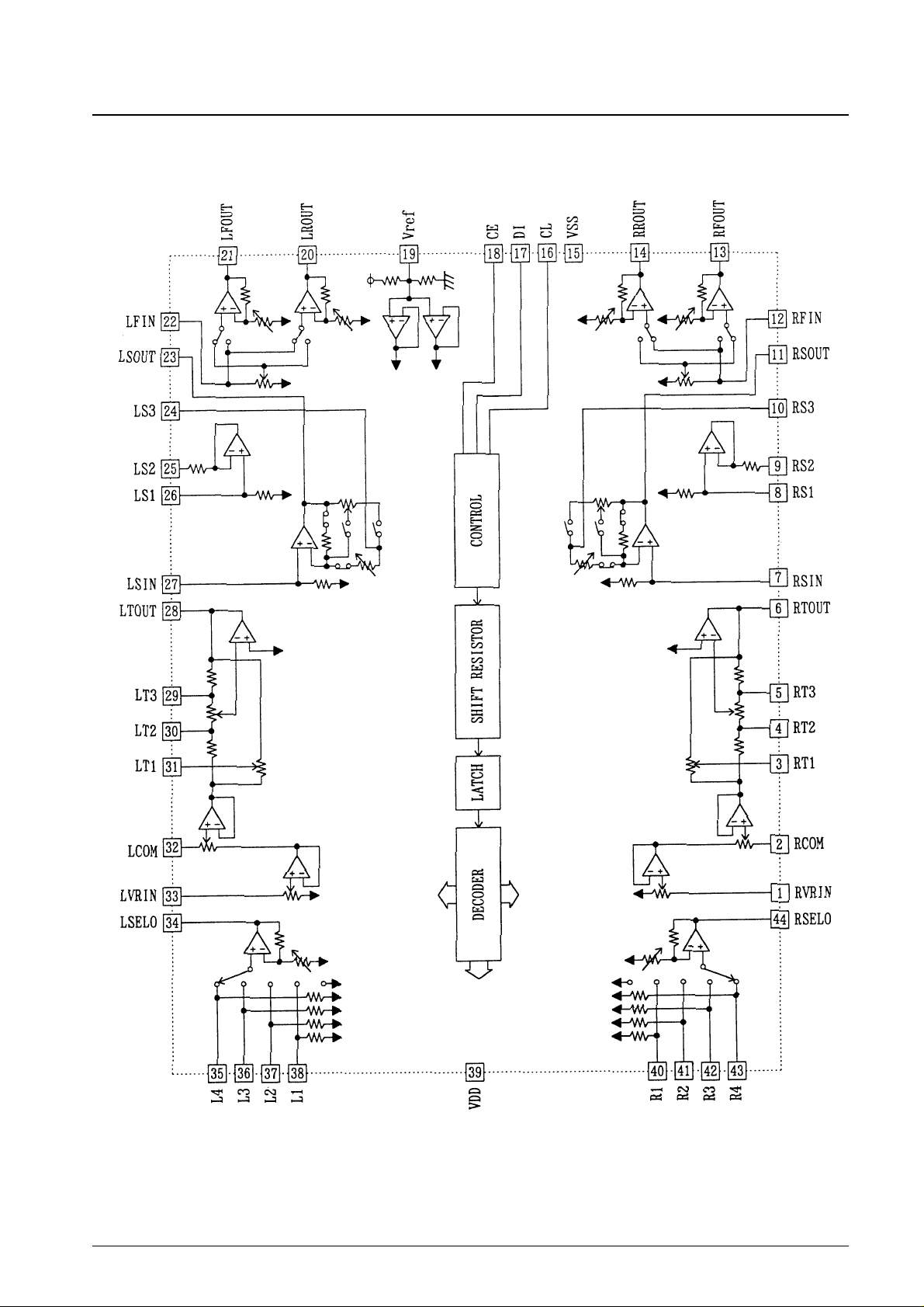
Equivalent Circuit Block Diagram
No. 5588-3/21
LC75373E
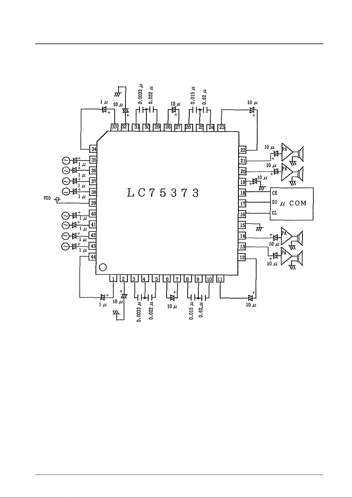
Sample Application Circuit
1. When super bass circuit 1 (Type GEQ) is used
No. 5588-4/21
LC75373E
Unit (capacitance: F)
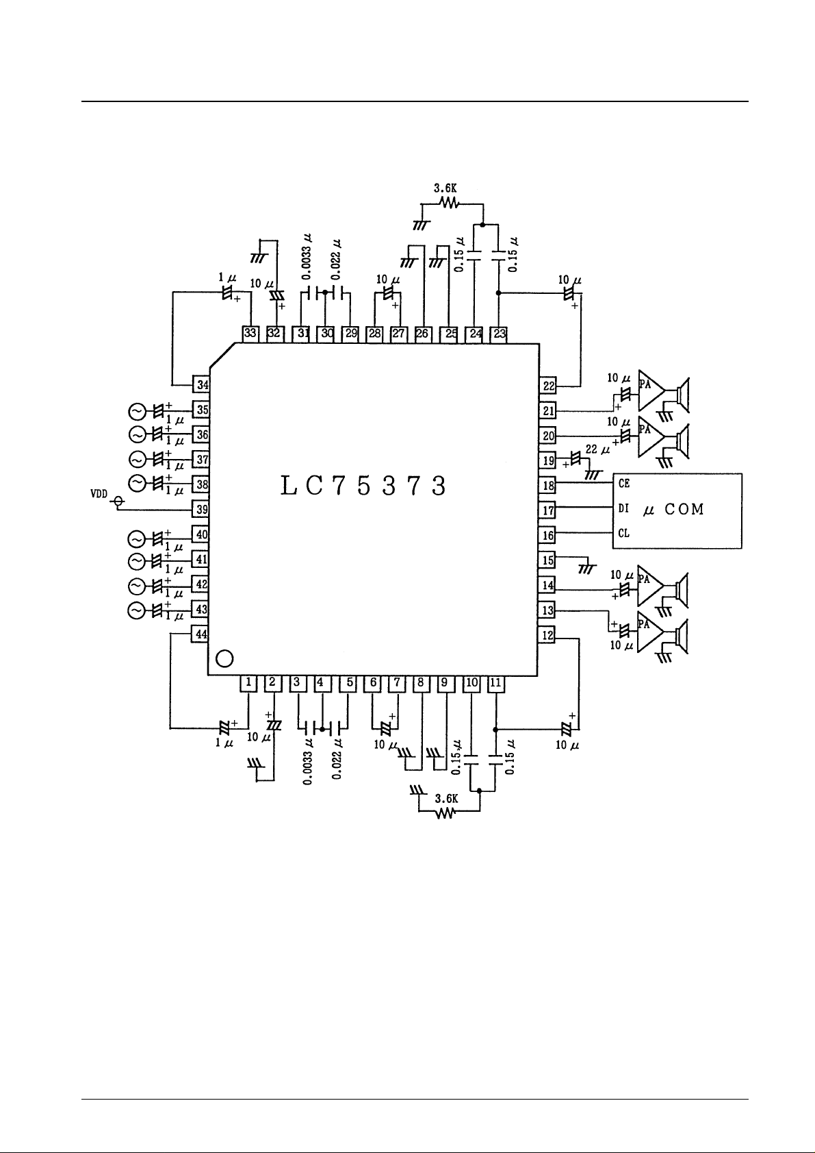
2. When super bass circuit 2 (Type T) is used
No. 5588-5/21
LC75373E
Unit (capacitance: F)
Unit (resistance: Ω)
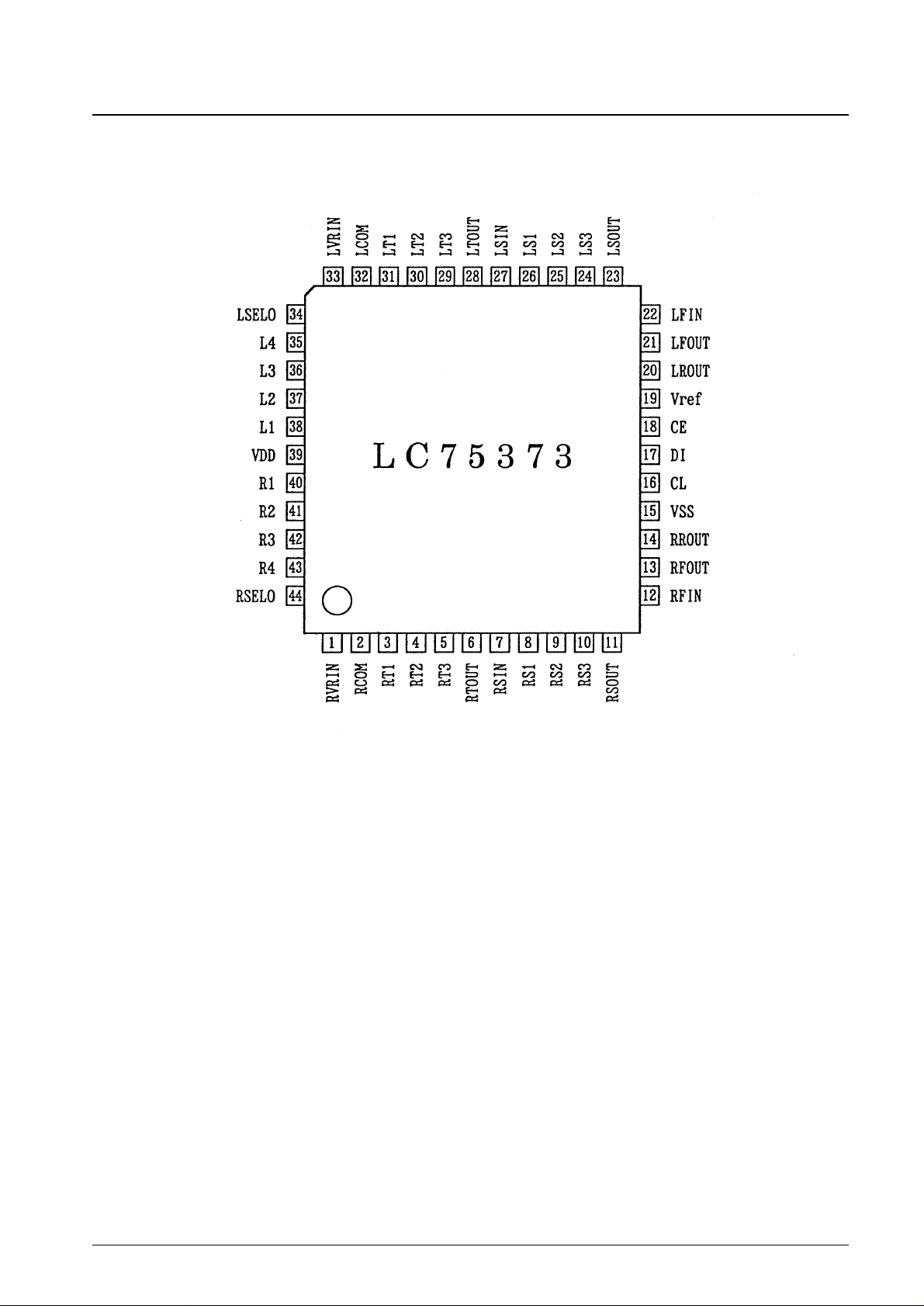
Pin Assignment
No. 5588-6/21
LC75373E
Top view

No. 5588-7/21
LC75373E
Pin Functions
Pin No. Symbol Function Note
19
20
21
14
13
22
12
28
6
31
30
29
3
4
5
26
25
24
8
9
10
33
1
Vref
LROUT
LFOUT
RROUT
RFOUT
LFIN
RFIN
LTOUT
RTOUT
LT1
LT2
LT3
RT1
RT2
RT3
LS1
LS2
LS3
RS1
RS2
RS3
LVRIN
RVRIN
• 1/2 V
DD
voltage generation block. A capacitor must be connected between
Vref and V
SS
to suppress power supply ripple.
• Fader outputs. The front and rear systems can be attenuated independently.
• Fader inputs
• Must be driven from low-impedance circuits.
• Tone control outputs
• Connections for the bass and treble compensation capacitors for the tone
control circuit
Connect high-band compensation capacitors between T1 and T2.
Connect low-band compensation capacitors between T2 and T3.
• Super bass compensation capacitors
• 4-dB volume control inputs
• These inputs must be driven from low-impedance circuits.
Continued on next page.
 Loading...