

Page 1
CMOS IC
3V Electronic Volume Control
Ordering number:ENN1374E
LC7533
SANYO Electric Co.,Ltd. Semiconductor Company
TOKYO OFFICE Tokyo Bldg., 1-10, 1 Chome, Ueno, Taito-ku, TOKYO, 110-8534 JAPAN
Any and all SANYO products described or contained herein do not have specifications that can handle
applications that require extremely high levels of reliability, such as life-support systems, aircraft’s
control systems, or other applications whose failure can be reasonably expected to result in serious
physical and/or material damage. Consult with your SANYO representative nearest you before using
any SANYO products described or contained herein in such applications.
SANYO assumes no responsibility for equipment failures that result from using products at values that
exceed, even momentarily, rated values (such as maximum ratings, operating condition ranges,or other
parameters) listed in products specifications of any and all SANYO products described or contained
herein.
Use
•Attenuation of signal.
Features
• CMOS process 3V typ. operation.
• Up/down operation is performed with SW input.
• 4-bit, 16-step counter. Step 6* is set with initial
input(INIT).
• Center tap provided.
• Maximum attenuation : –60dB or less.
• Attenuation curve : Pseudo curve A. Left/right simultaneous setting.
*
: Step 6 means mode 6.
Specifications
Absolute Maximum Ratings at Ta = 25˚C
retemaraPlobmySsnoitidnoCsgnitaRtinU
egatlovylppusmumixaMV
egatlovylppuSV
noitapissidrewopelbawollAxamdP 001Wm
erutarepmetgnitarepOrpoT 57+ot03–
erutarepmetegarotSgtsT 521+ot04–
xam VSS6otV
DD
I
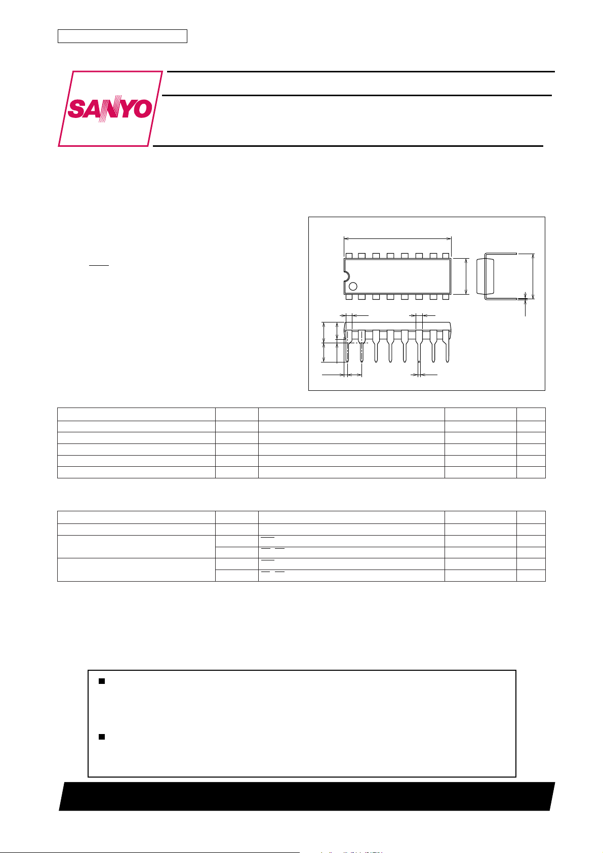
Package Dimensions
(unit:mm)
3006C-DIP16
[LC7533]
19.0
16
1
3.65max
3.4
(0.61)
1.09
(3.0)
0.51min
2.54
1.2
0.48
9
6.4
8
SANYO : DIP16
VSSVot
7.62
0.25
V
DD
˚C
˚C
Allowable Operating Conditions at Ta = 25˚C
retemaraPlobmySsnoitidnoCsgnitaRtinU
egatlovylppuSV
egatlovlevel-hgihtupnI
egatlovlevel-woltupnI
DD
V
1HI
V
2HI
V
1LI
V
2LI
nipEC,TINIV7.0
nipRC,ND,PUV9.0
EC,TINI V3.0ot0
RC,ND,PUV
51501TN (KT)/N111JN/1250TA/7048YT/7235MW/9034KI/9303KI,TS No.1374–1/3
0.5ot1.2V
Vot
DD
DD
SS
V
DD
Vot
V
DD
V
DD
V1.0ot
V
DD
Page 2
Electrical Characteristics at Ta = 25˚C
retemaraPlobmySsnoitidnoC
noitrotsidlangiS
edomnoitaunettatatuptuOX
emityaledtimsnartlangiSdtdaolon,TUOdnaNIneewteB1sµ
ecnadepmitupnIr
egatlovesiontuptuOV
tnerruclevel-hgihtupnII
tnerruclevel-woltupnII
ecnalabnoitaunettA
ecnalablennahC
niardtnerruC
slennahcneewtebklatssorCTC
htdiweslupmuminiM
Note 1 (1) ∆V=20log10 V
V
: OUT1(OUT2) output level
OUT
V
: Standard output level
TYP
(2) Satisfy V
OUT
OUT/VTYP
(STEP N) < V
T
OUT
DHT
V
1
DHT
V
2
TUO
i
V
ON
HI
LI
∆V
∆V
O
I
I
T
V
DD
DD
V
PUKCAB
V
ND/PU
TINI
(STEP N + 1)
LC7533
sgnitaR
nimpytxam
R,V3=
DD
DD
DD
)2etoN(
DD
DD
DD
nipTINI2sµ
k05= Ω zHk1=f,5.0%
L
R,V1.2=
k05= Ω zHk1=f,1%
L
k15,zHk1,tupnimBd0 Ω daol06–Bd
ylnoEC,ND,PU001004kΩ
R,V3=
k05= Ω ”0“PETS,8Vµ
L
V,nipEC
V,V3=
DD
V,nipND,PU
V,V5.1=
V3=04Aµ
I
V,V3=
DD
V=EC,V3=
DD
V=EC,V3=
SS
=– V,V5.1
SS
V0=55–Aµ
I
V=TINI,
DD
V=TINI,
DD
M
k1:tupniedistset,tupni Ω trohs
Note 2 (1) ∆VO=20log10 V
)1etoN(”0“PETSnahtrehto,2,1TUOsniP2–02+Bd
”0“PETSnahtrehto,2,1TUOsnipneewteB
NEPO:sniprehto,1Am
NEPO:sniprehto,1Aµ
k1=f,V0= Ω smrV1,
nipND,PU)elcycnoitallicsoRC(=T5.1
2–2+Bd
OUT1/VOUT2
58Bd
T
tinU
sm
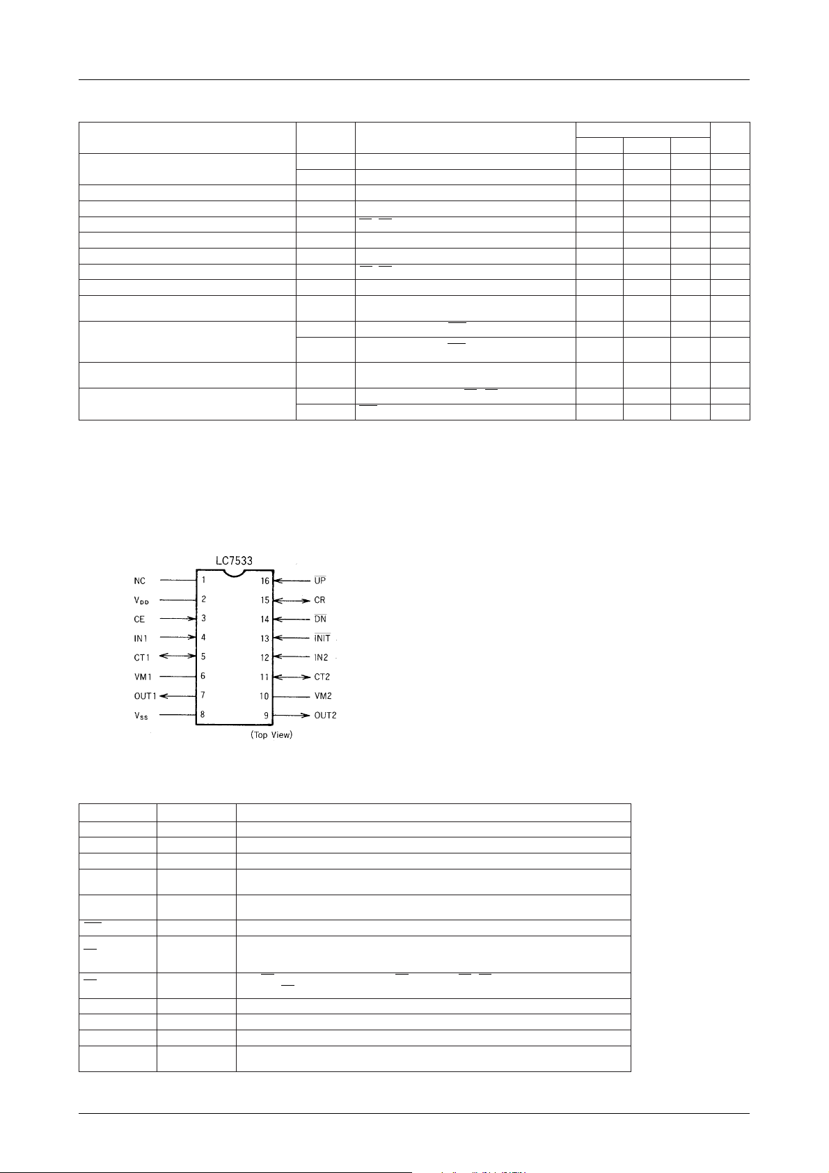
Pin Assignment
Pin Description
emaNniPrebmuNniPnoitpircseD
2NI,1NI21,4lortnocemulovrofniptupnI
2TUO,1TUO9,7lortnocemulovrofniptuptuO
V1MV,
2M
C1TC,
2T
EC3
TINI31.dehcaersipetsht6eht,”L“ottesnehW.niplaitinI
PU61
ND41
RC51.sdnepedpetsfoetarehthcihwnoC,RgnitcennocrofniP
V
DD
V
SS
CN1
01,6V2/1,ylppuselgnismorfdetareponehW.nipsaiB
11,5
.edom
2)+(nipylppusrewoP
8dnuorG
Note 1 : No bonding exists on the inside of NC pin.
It is recommended that the outside should
be shorted to VDD, VSS, etc. on the printed
circuti board.
DD
.dellortnocebnacssenduol
.noitisopBSMehttaspotspetsehT.tnemomtahttadehcaer
.noitisopBSLehttaspotspetsehT.ytiroirpnevigsiPUeht,emit
VotdetcennoC
Vro
DD
SS
.nipCNfoedisniehtnostsixegnidnoboN
.dednemmocersi
.nipsihtotdeilppasi
eht,nipsihtotRdnaCgnitcennocyB.lortnocemulovforetnecehttadedivorpnippaT
pukcabta”L“ebtsumnipsihT.decudersiniardtnerruceht,”L“ottessinipsihtnehW
nehW.puseogemulovehtdnasesirpetseht,llafotedamsinipsihtnolevelehtnehW
petsatapugniogspotsemuloveht,”H“ottesfi;puseogemuloveht,”L“tadleh
emasehtta”L“otteseraND,PUehtnehw.PUfoesreverehtsinoitarepoNDehT
No.1374–2/3
Page 3

LC7533
Equivalent Circuit Block Diagram
[Common to LC7533]
Sample Application Circuit
[LC7533 DIP16]
Specifications of any and all SANYO products described or contained herein stipulate the performance,
characteristics, and functions of the described products in the independent state, and are not guarantees
of the performance, characteristics, and functions of the described products as mounted in the customer's
products or equipment. To verify symptoms and states that cannot be evaluated in an independent device,
the customer should always evaluate and test devices mounted in the customer's products or equipment.
SANYO Electric Co., Ltd. strives to supply high-quality high-reliability products. However, any and all
semiconductor products fail with some probability. It is possible that these probabilistic failures could
give rise to accidents or events that could endanger human lives, that could give rise to smoke or fire,
or that could cause damage to other property. When designing equipment, adopt safety measures so
that these kinds of accidents or events cannot occur. Such measures include but are not limited to protective
circuits and error prevention circuits for safe design, redundant design, and structural design.
In the event that any or all SANYO products(including technical data,services) described or
contained herein are controlled under any of applicable local export control laws and regulations,
such products must not be exported without obtaining the export license from the authorities
concerned in accordance with the above law.
No part of this publication may be reproduced or transmitted in any form or by any means, electronic or
mechanical, including photocopying and recording, or any information storage or retrieval system,
or otherwise, without the prior written permission of SANYO Electric Co. , Ltd.
Any and all information described or contained herein are subject to change without notice due to
product/technology improvement, etc. When designing equipment, refer to the "Delivery Specification"
for the SANYO product that you intend to use.
Information (including circuit diagrams and circuit parameters) herein is for example only ; it is not
guaranteed for volume production. SANYO believes information herein is accurate and reliable, but
no guarantees are made or implied regarding its use or any infringements of intellectual property rights
or other rights of third parties.
This catalog provides information as of May, 2001. Specifications and information herein are subject to
change without notice.
No.1374–3/3
 Loading...