

Ordering number : EN5913
101698RM (OT) No. 5913-1/10
Overview
The LC75281E is a four-band stereo parametric equalizer.
A parametric equalizer is a fully general equalizer that
allows all three parameters that define an equalizer’s
characteristics, i.e., the center frequency, gain, and Q, to
be set independently.
Functions
• Four-band (low, low mid, high mid, and high) left and
right channels parametric equalizer
• For each band:
Center frequency: 11 positions
Gain: 13 positions in ±2dB steps
Q: Variable over 8 positions
• The center frequency, gain, and Q control settings are
set using serial data input in the CCB format.
Features
• A parametric equalizer with the following features can
be implemented with just two ICs: this IC and a
microcontroller.
• The center frequency, gain, and Q can be controlled by a
single operation.
• Memory recall by a single operation can be implemented using preset values.
• Either shelving or peaking characteristics can be
selected for the low band.
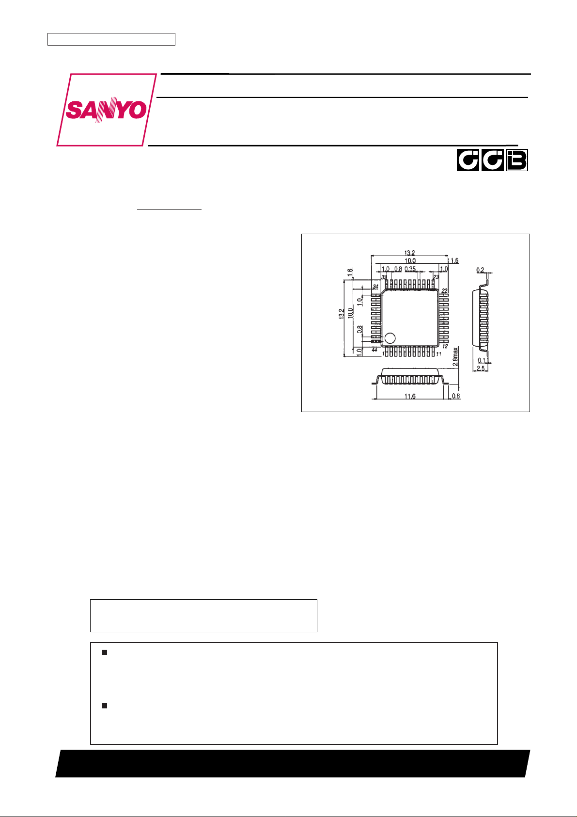
Package Dimensions
unit: mm
3159-QFP64E
LC75281E
SANYO Electric Co.,Ltd. Semiconductor Bussiness Headquarters
TOKYO OFFICE Tokyo Bldg., 1-10, 1 Chome, Ueno, Taito-ku, TOKYO, 110-8534 JAPAN
Parametric Equalizer System
CMOS IC
Any and all SANYO products described or contained herein do not have specifications that can handle
applications that require extremely high levels of reliability, such as life-support systems, aircraft’s
control systems, or other applications whose failure can be reasonably expected to result in serious
physical and/or material damage. Consult with your SANYO representative nearest you before using
any SANYO products described or contained herein in such applications.
SANYO assumes no responsibility for equipment failures that result from using products at values that
exceed, even momentarily, rated values (such as maximum ratings, operating condition ranges, or other
parameters) listed in products specifications of any and all SANYO products described or contained
herein.
SANYO: QFP64E (QIP64E)
[LC75281E]
• CCB is a trademark of SANYO ELECTRIC CO., LTD.
• CCB is SANYO’s original bus format and all the bus
addresses are controlled by SANYO.
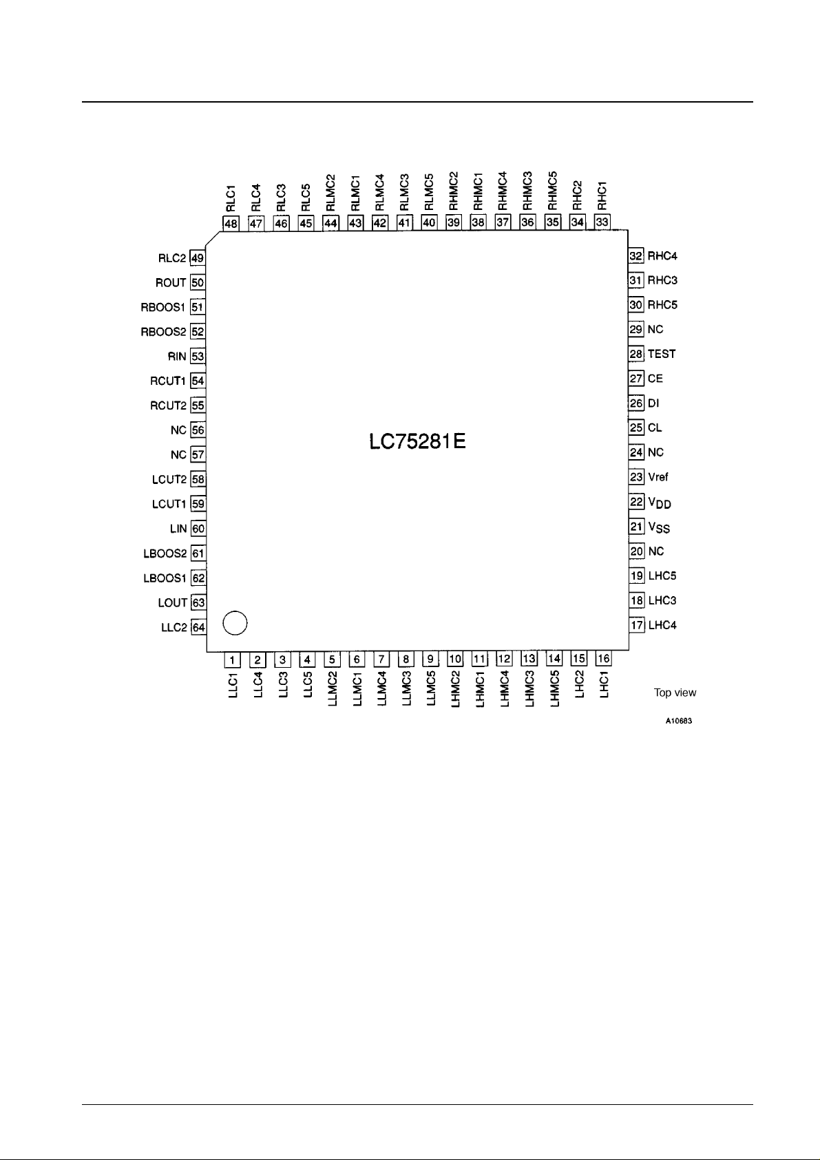
Pin Assignment
No. 5913-2/10
LC75281E

Specifications
Absolute Maximum Ratings at Ta = 25°C, VSS= 0 V
Allowable Operating Ranges at Ta = –40 to +85°C, VSS= 0 V
Electrical Characteristics at Ta = 25°C, f = 1 kHz, VDD= 8 V, VSS= 0 V
Pin Functions
No. 5913-3/10
LC75281E
Parameter Symbol Conditions Ratings Unit
Maximum supply voltage V
DD
max 10.5 V
Maximum input voltage
V
IN
1 max LIN, RIN 0 to V
DD
V
V
IN
2 max CL, CE, DI 0 to V
DD
V
Allowable power dissipation Pd max Ta ≤ 85°C 300 mW
Operating temperature Topr –40 to +85 °C
Storage temperature Tstg –50 to +125 °C
Parameter Symbol Conditions
Ratings
Unit
min typ max
Supply voltage V
DD
6.0 9.0 V
High-level input voltage V
IH
CL, CE, DI 4.0 V
DD
V
Low-level input voltage V
IL
CL, CE, DI V
SS
1.0 V
Input voltage range V
IN
LIN, RIN 0 V
DD
V
Load resistance R
L
LOUT, ROUT, MIXOUT 1 kΩ
Input pulse width tøw CL 1 µs
Setup time tsetup CL, CE, DI 1 µs
Hold time thold CL, CE, DI 1 µs
Operating frequency fopg CL 500 kHz
Parameter Symbol Conditions
Ratings
Unit
min typ max
Current drain I
DD
V
DD
36 50 mA
Output voltage V
O
LOUT, ROUT: THD = 1% 2.2 Vrms
THD1 LOUT, ROUT: Vo = Flat, V
IN
= 0 dBV 0.005 0.01 %
Total harmonic distortion
THD2
LOUT, ROUT: Vo = Boost,
0.1 1 %
All bands +2 dB, V
IN
= –15 dBV
V
N
1
LOUT, ROUT: Vo = Flat,
7 15 µs
Rg = 1 kΩ, IHF-A filters
V
N
2
LOUT, ROUT: Vo = Flat,
13 µs
Rg = 1 kΩ, DIN filters
LOUT, ROUT, Rg = 1 k
Ω, f0 = f1, Q = Q1
Output noise voltage
V
N
3
IHF-A filter, all bands at full boost, with the external
58 µs
constants the same as those for the center
frequency (example 1)
LOUT, ROUT, Rg = 1 kΩ, f0 = f1, Q = Q1
V
N
4
IHF-A filters, all bands at full cut, with the external
23 µs
constants the same as those for the center frequency
(example 1)
Crosstalk between inputs CT V
IN
= 1 Vrms, f = 1 kHz 60 80 dB
High-level input current I
IH
CL, DI, CE, VIN= 9 V 1 µA
Low-level input current I
IL
CL, DI, CE, VIN= 0 V –1 µA
All bands
DC variation V
DC
G = +12 dB, Q: Setting switched from Q1 to Q2
–10 +10 mV
With the external constants the same as those for the
center frequency (example 1) shown on page 7.
Pin No. Pin Function
64 LLC2
1 LLC1
2 LLC4
3 LLC3
4 LLC5
5 LLMC2
6 LLMC1
7 LLMC4
8 LLMC3
Left channel low band control block.
External capacitor connections.
Left channel low mid band control block.
External capacitor connections.
Continued on next page.
 Loading...