

SANYO LC74794M, LC74794 Datasheet

Overview
The LC74794 and LC74794M are CMOS LSIs for onscreen display, a function that displays characters and
patterns on a TV screen under microprocessor control.
They feature a built-in PDC/VPS/UDT interface circuit.
These LSIs support 12 × 18 dot characters and can display
12 lines by 24 characters of text.
Features
• Display format: 24 characters by 12 rows (Up to 288
characters)
• Character format: 12 (horizontal) × 18 (vertical) dots
• Character sizes: Three sizes each in the horizontal and
vertical directions
• Characters in font: 128
• Initial display positions: 64 horizontal positions and 64
vertical positions
• Blinking: Specifiable in character units
• Blinking types: Two periods supported: 1.0 second and
0.5 second
• Blanking: Over the whole font (12 × 18 dots)
• Background color
— Background coloring: 8 colors (internal synchronization
mode): 4fsc
— Background coloring: 6 colors (internal synchronization
mode): 2fsc
— Blue background only: NTSC
• Line background color
— Can be set for 3 lines
— Line background coloring: 8 colors (internal synchro-
nization mode): 4fsc
— Line background coloring: 6 colors (internal synchro-
nization mode): 2fsc
• External control input: 8-bit serial input format
• On-chip sync separator and AFC circuits
• PDC/VPS/UDT interface circuit
• Composite video output in the PAL or NTSC format
Package Dimensions
unit: mm
3196-DIP30SD
unit: mm
3216A-MFP30S
CMOS LSI
Ordering number : EN*5557
22897HA (OT)/No. 5557-1/30
Preliminary
SANYO: DIP30SD
[LC74794]
SANYO: MFP30S
[LC74794M]
SANYO Electric Co.,Ltd. Semiconductor Bussiness Headquarters
TOKYO OFFICE Tokyo Bldg., 1-10, 1 Chome, Ueno, Taito-ku, TOKYO, 110 JAPAN
On-Screen Display Controller LSI
LC74794, 74794M
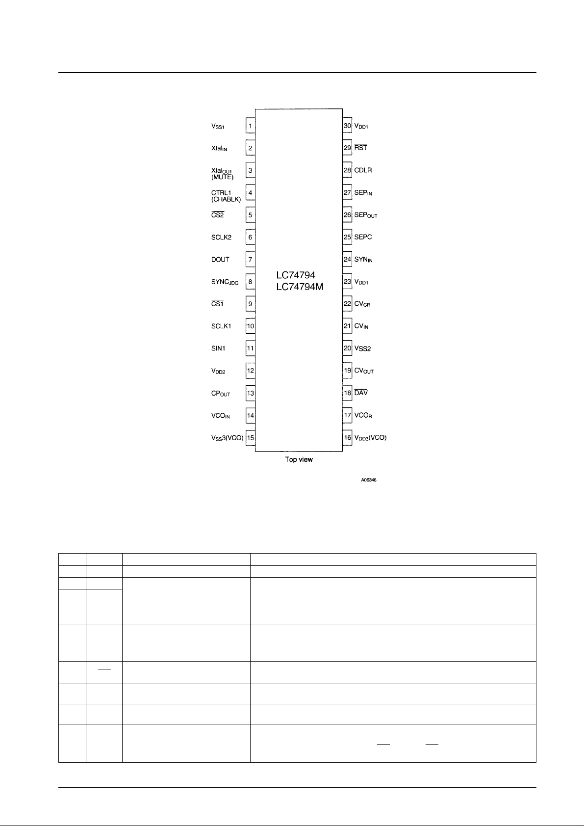
Pin Assignment
No. 5557-2/30
LC74794, 74794M
Pin Functions
Pin no. Pin Function Notes
1 V
SS
1 Ground Ground connection (digital system ground)
2 Xtal
IN
Crystal oscillator
These pins are used either to connect a crystal and capacitor to form an external crystal
3
Xtal
OUT
(MUTE input)
oscillator to generate internal synchronizing signals, or to input an external clock signal (2fsc
(MUTE)
or 4fsc). As a mask option, the XtalOUT pin can be set to function as the MUTE input pin.
When the MUTE pin is set low, the video output is held at the pedestal level. (A pull-up
resistor is built in so the input has hysteresis characteristics.)
Switches the mode between external clock input and crystal oscillator operation. A low level
4
CTRL1 Crystal oscillator input switching selects crystal oscillator operation and a high level selects external clock input. As a mask
(CHABLK) (CHABLK output) option, the CTRL1 input pin can be set to function as the CHABLK (character · border)
output. This is a 3-value output.
5 CS2 Enable input 2
PDC/VPS data output enable input. Data output is enabled by a low-level input. (A pull-up
resistor is built in so the input has hysteresis characteristics.)
6 SCLK2 Clock input 2
Clock input for PDC/VPS data output
(A pull-up resistor is built in so the input has hysteresis characteristics.)
7 DOUT Data output
PDC/VPS data output
(This is either an n-channel open-drain output or a CMOS output.)
Outputs the state of the external synchronizing signal presence/absence judgment.
8 SYNC
JDG
External synchronizing signal judgment Outputs a high level when synchronizing signals are present.
output Outputs the crystal oscillator clock when CS1 is low and RST is low. (This signal is not
output on command resets.)
Continued on next page.
No. 5557-3/30
LC74794, 74794M
Continued from preceding page.
Pin no. Pin Function Notes
Enable input for OSD serial data input
9 CS1 Enable input 1 Serial data input is enabled by a low-level input.
(A pull-up resistor is built in so the input has hysteresis characteristics.)
10 SCLK1 Clock input 1
Serial data clock input
(A pull-up resistor is built in so the input has hysteresis characteristics.)
11 SIN1 Data input 1 Serial data input (A pull-up resistor is built in so the input has hysteresis characteristics.)
12 V
DD
2 Power supply Composite video signal level adjustment power supply (analog system power supply)
13 CP
OUT
Charge pump output The charge pump output. Connect a low-pass filter to this pin.
14 VCO
IN
Oscillator control voltage input VCO control voltage input
15 V
SS
3 Ground Ground (VCO ground)
16 V
DD
3 Power supply (+5 V) Power supply (+5 V: VCO power supply)
17 VCO
R
Oscillator range adjustment Connection for the VCO range adjustment resistor
18 DAV Data present output Outputs a low level when PDC/VPS data has been received.
19 CV
OUT
Video signal output Composite video signal output
20 V
SS
2 Ground Ground (analog system ground)
21 CV
IN
Video signal input Composite video signal input
22 CV
CR
Video signal input SECAM chrominance signal input
23 V
DD
1 Power supply (+5 V) Power supply (+5 V: digital system power supply)
24 SYN
IN
Sync separator circuit input Internal sync separator circuit video signal input
25 SEPC Sync separator circuit adjustment Internal sync separator circuit adjustment input
Composite synchronizing signal output for the built-in sync separator circuit. Can be
26 SEP
OUT
Composite synchronizing signal output switched to function as an output for the signal (high or ST. pulse) due to MOD0 by setting
SEL0 high.
Inputs the vertical synchronizing signal created by integrating the SEP
OUT
pin output
27 SEPINVertical synchronizing signal input
signal.
An integration circuit must be connected to the SEP
OUT
pin. This pin must be tied to VDD1
if unused.
28 CDLR Background color phase adjustment Background color phase adjustment resistor connection
29 RST Reset input
System reset input
A pull-up resistor is built in so the input has hysteresis characteristics.
30 V
DD
1 Power supply (+5 V) Power supply (+5 V: digital system power supply)

No. 5557-4/30
LC74794, 74794M
Parameter Symbol Conditions Ratings Unit
Supply voltage V
DD
VDD1 and VDD2 VSS– 0.3 to VSS+ 7.0 V
Input voltage V
IN
All input pins VSS– 0.3 to VDD+ 0.3 V
Output voltage V
OUT
DAV, DOUT, SEP
OUT
, and SYNC
JDG
VSS– 0.3 to VDD+ 0.3 V
Allowable power dissipation Pd max 350 mW
Operating temperature Topr –30 to +70 °C
Storage temperature Tstg –40 to +125 °C
Specifications
Absolute Maximum Ratings at Ta = 25°C
Parameter Symbol Conditions
Ratings
Unit
min typ max
Supply voltage
V
DD
1 VDD1 and VDD2 4.5 5.0 5.5 V
V
DD
2 VDD2 5.5 5.0 1.27 VDD1 V
V
IH
1
RST, CS1, CS2, SIN1, SCLK1, SCLK2,
0.8 VDD1 VDD1 + 0.3 V
Input high-level voltage
and MUTE
V
IH
2 CTRL1 0.7 VDD1 VDD1 + 0.3 V
V
IL
1
RST, CS1, CS2, SIN1, SCLK1, SCLK2,
VSS– 0.3 0.2 VDD1 V
Input low-level voltage
and MUTE
V
IL
2 CTRL1 VSS– 0.3 0.3 VDD1 V
Pull-up resistance R
PU
RST, CS1, CS2, SIN1, SCLK1, SCLK2,
25 50 90 kΩ
and MUTE
Composite video signal input voltage
V
IN
1 CVINand CVCR; VDD1 = 5 V 2.0 Vp-p
V
IN
2 SYNIN; VDD1 = 5 V 1.5 2.0 2.5 Vp-p
Input voltage V
IN
3
Xtal
IN
(in external clock input mode)
0.10 5.0 Vp-p
fin = 2 fsc or 4 fsc ; V
DD
1 = 5 V
Oscillator frequency
F
OSC
1 XtalINand Xtal
OUT
oscillator pins (2 fsc: PAL) 8.867 MHz
F
OSC
2 XtalINand Xtal
OUT
oscillator pins (4 fsc: PAL) 17.734 MHz
Allowable Operating Ranges at Ta = –30 to +70°C
Note: When the XtalINpin is used in clock input mode, extreme care must be taken to prevent noise from entering the input signal.
Parameter Symbol Conditions
Ratings
Unit
min typ max
Input off leakage current I
leak
1 CVINand CV
CR
1 µA
Output off leakage current I
leak
2 CV
OUT
1 µA
Output high-level voltage V
OH
1
DAV, DOUT, SEP
OUT
, CP
OUT
, SYNC
JDG
;
3.5 V
V
DD
1 = 4.5 V, IOH= –1.0 mA
Output low-level voltage V
OL
1
DAV, DOUT, SEP
OUT
, CP
OUT
, SYNC
JDG
;
1.0 V
V
DD
1 = 4.5 V, IOL= 1.0 mA
CHABLK ; V
DD
1 = 5.0 V H 3.3 5.0 V
Three-value output voltage V
O
M 1.8 2.3 V
L 0 0.8 V
RST, CS1, CS2, SIN, SCLK1, SCLK2,
I
IH
CTRL1, MUTE, SEPIN, and VCO
IN
1 µA
Input current
V
IN
= VDD1
I
IL
CTRL1, SEPIN, and VCOIN; VIN= VSS1 –1 µA
I
DD
1
V
DD
1; with all outputs open
40 mA
Operating current drain
Xtal : 17.734 MHz, VCO : 27 MHz
I
DD
2 VDD2; VDD2 = 5 V 20 mA
CV
OUT
; VDD1 = 5.0 V ➀ 0.80 V
SYNC level V
SN
VDD2 = 5.0 V ➁ 1.00 V
➂ 1.30 V
CV
OUT
; VDD1 = 5.0 V ➀ 1.37 V
Pedestal level V
PD
VDD2 = 5.0 V ➁ 1.57 V
➂ 1.87 V
CV
OUT
; VDD1 = 5.0 V ➀ 1.07 V
Color burst low level V
CBL
VDD2 = 5.0 V ➁ 1.27 V
➂ 1.57 V
Electrical Characteristics at Ta = –30 to +70°C, VDD1 = 5 V unless otherwise specified.
Continued on next page.

No. 5557-5/30
LC74794, 74794M
Parameter Symbol Conditions
Ratings
Unit
min typ max
CV
OUT
; VDD1 = 5.0 V ➀ 1.67 V
Color burst high level V
CBH
VDD2 = 5.0 V ➁ 1.87 V
➂ 2.17 V
CV
OUT
; VDD1 = 5.0 V ➀ 1.23 (1.16) V
Background color low level V
RSL
VDD2 = 5.0 V ➁ 1.43 (1.36) V
➂ 1.73 (1.66) V
CV
OUT
; VDD1 = 5.0 V ➀ 2.37 (2.01) V
Background color high level V
RSH
VDD2 = 5.0 V ➁ 2.57 (2.21) V
➂ 2.87 (2.51) V
CV
OUT
; VDD1 = 5.0 V ➀ 1.50 V
Frame level 0 V
BK
0 VDD2 = 5.0 V ➁ 1.70 V
➂ 2.00 V
CV
OUT
; VDD1 = 5.0 V ➀ 2.08 V
Frame level 1 V
BK
1 VDD2 = 5.0 V ➁ 2.28 V
➂ 2.58 V
CV
OUT
; VDD1 = 5.0 V ➀ 2.65 V
Character level V
CHA
VDD2 = 5.0 V ➁ 2.85 V
➂ 3.15 V
Continued from preceding page.
Notes:➀ When the sync level is 0.8 V.
➁ When the sync level is 1.0 V.
➂ When the sync level is 1.3 V.
The values in parentheses for the background color high and low levels are the values for a blue background.
Note: Timings follow those for OSD write when the CMOS output circuit is used.
Parameter Symbol Conditions
Ratings
Unit
min typ max
Minimum input pulse width
t
W(SCLK)
SCLK1 200 ns
t
W(CS1)
CS1 (The period when CS1 is high) 1 µs
Data setup time
t
SU(CS1)
CS1 200 ns
t
SU(SIN)
SIN1 200 ns
Data hold time
t
h(CS1)
CS1 2 µs
t
h(SIN)
SIN1 200 ns
One word write time
t
word
The time to write 8 bits of data 4.2 µs
t
wt
The RAM data write time 1 µs
Timing Characteristics at Ta = –30 to +70°C, VDD1 = 5 ± 0.5 V
OSD write (See Figure 1.)
Parameter Symbol Conditions
Ratings
Unit
min typ max
t
CKCY
SCLK2 2 µs
Minimum input pulse width t
CKL
SCLK2 1 µs
t
CKH
SCLK2 1 µs
Setup time t
ICK
SCLK2 10 µs
Output delay time t
CKO
DOUT 0.5 µs
PDC/VPS reads (For the n-channel open-drain output circuit. See Figure 2.)
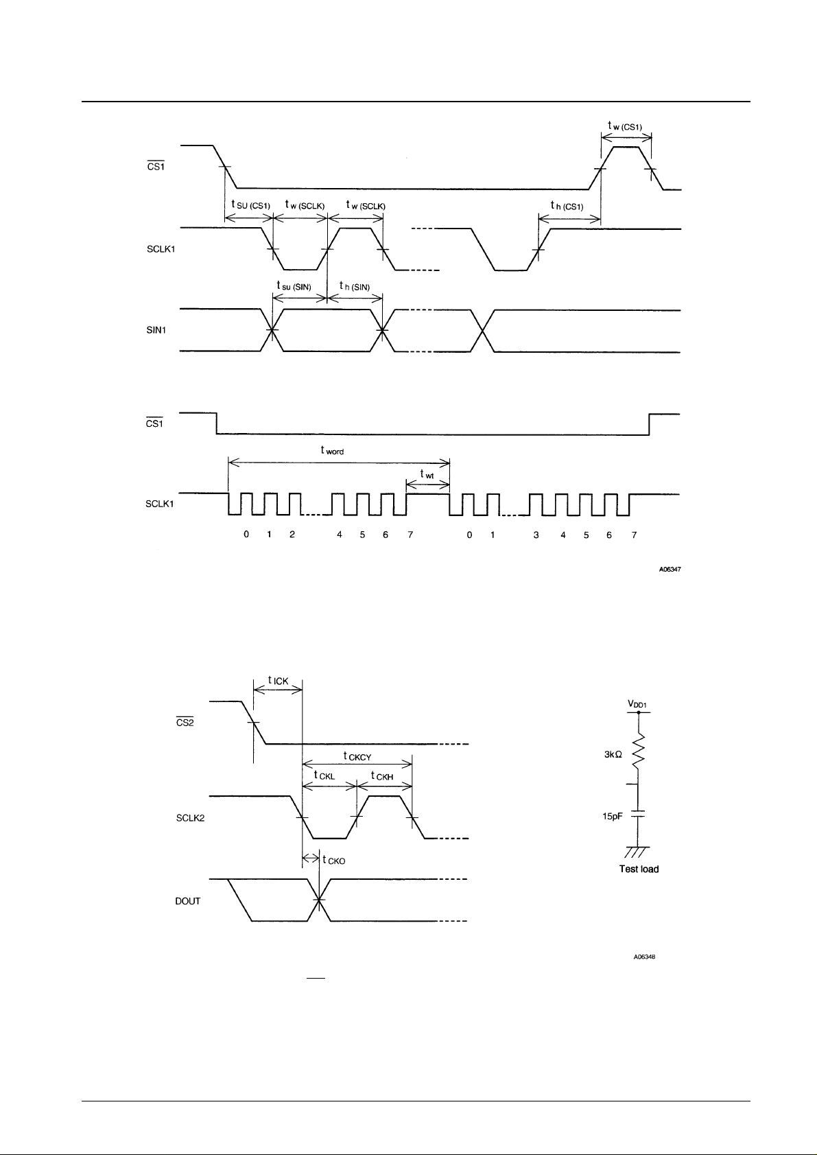
Figure 1 OSD Serial Data Input Timing
Figure 2 PDC/VPS Serial Output Test Conditions (For the n-channel open-drain output)
Note: DOUT goes to the high-impedance state while CS2 is high.
No. 5557-6/30
LC74794, 74794M

System Block Diagram
No. 5557-7/30
LC74794, 74794M

No. 5557-8/30
LC74794, 74794M
Display Control Commands
Display control commands have an 8-bit format and are transferred using the serial input function. Commands consist of
a command identification code in the first byte and command data in the following bytes. The following commands are
supported.
1 COMMAND0: Display memory (VRAM) write address setup command
2 COMMAND1: Display character data write command
3 COMMAND2: Vertical display start position and vertical character size setup command
4 COMMAND3: Horizontal display start position and horizontal character size setup command
5 COMMAND4: Display control setup command
6 COMMAND5: Display control setup command
7 COMMAND6: Synchronizing signal detection setup command
8 COMMAND7 to COMMAND12: Display control setup commands
9 COMMAND13 to COMMAND17: VPS/PDC commands
Display Control Command Table
Once written, the command identification code in the first byte is stored until the next first byte is written. However,
when the display character data write command (COMMAND1) is written, the LC74794/M locks into the display
character data write mode, and another first byte cannot be written.
When the CS1 pin is set high, the LC74794/M is set to the COMMAND0 (display memory write address setup mode)
state.
First byte Second byte
Command
Command identification code
Data Data
7 6 5 4 3 2 1 0 7 6 5 4 3 2 1 0
COMMAND0 1 0 0 0 V3 V2 V1 V0 0 0 0 H4 H3 H2 H1 H0
Write address setup
COMMAND1 1 0 0 1 0 0 0 0 at c6 c5 c4 c3 c2 c1 c0
Character write
COMMAND2 1 0 1 0 VS VS VS VS 0 FS VP VP VP VP VP VP
Vertical character size and 21 20 11 10 5 4 3 2 1 0
vertical display start position
COMMAND3 1 0 1 1 HS HS HS HS 0 HP HP HP HP HP HP
Horizontal character size and 21 20 11 10 5 4 3 2 1 0
horizontal display start position
COMMAND4 1 1 0 0 TST RAM OSC SYS 0 BLK BLK BLK BK BK RV DSP
Display control MOD ERS STP RST 2 1 0 1 0 ON
COMMAND5 1 1 0 1 NP1 NP0 NON INT 0 0 HLF BCL CB PH PH PH
Display control INT 2 1 0
COMMAND6 1 1 1 0 SEL MOD DIS MUT 0 RN RN RN SN SN SN SN
Synchronizing signal detection 0 0 LIN 2 1 0 3 2 1 0
COMMAND7 1 1 1 1 0 0 0 0 0 CIN CIN VNP VSP MSK MSK EGL
Display control SEL CTL SEL SEL ERS SEL
COMMAND8 1 1 1 1 0 0 0 1 0 LNA LNA LNA LNA LPA LPA LPA
Display control 3 2 1 0 2 1 0
COMMAND9 1 1 1 1 0 0 1 0 0 LNB LNB LNB LNB LPB LPB LPB
Display control 3 2 1 0 2 1 0
COMMAND10 1 1 1 1 0 0 1 1 0 LNC LNC LNC LNC LPC LPC LPC
Display control 3 2 1 0 2 1 0
COMMAND11 1 1 1 1 0 1 0 0 0 0 0 0 LNC MOD LNB MOD
Display control SEL 3 SEL 2
COMMAND12 1 1 1 1 0 1 0 1 0 0 0 0 0 SEL SEL CTL
Display control 2 1 3
COMMAND13 1 1 1 1 0 1 1 0 0 CPA CPA 0 VPM VPM VPM VPM
VPS/PDC control 1 0 3 2 1 0
COMMAND14 1 1 1 1 0 1 1 1 0 0 0 HBS HBS BMS EMS DCE
VPS/PDC control 2 1
COMMAND15 1 1 1 1 1 0 0 0 0 0 ECV ECV ECV ECV ECV ECV
VPS/PDC control 15 14 13 12 11 5
COMMAND16 1 1 1 1 1 0 0 1 0 ECP ECP ECP ECP ECP ECP ECP
VPS/PDC control 19 18 17 16 15 14 13
COMMAND17 1 1 1 1 1 0 1 0 0 0 ECP ECP ECP ECP ECP ECP
VPS/PDC control 25 24 23 22 21 20

No. 5557-9/30
LC74794, 74794M
COMMAND0 (Display memory write address setup command)
First byte
DA
Register
Contents
Notes
0 to 7 State Function
7 — 1
6 — 0
5 — 0
4 — 0
3 V3
0
1
2 V2
0
1
1 V1
0
1
0 V0
0
1
Command 0 identification code
Sets the display memory write address.
Display memory line address (0 to B hexadecimal)
COMMAND1 (Display character data write setup command)
First byte
DA
Register
Contents
Notes
0 to 7 State Function
7 — 1
6 — 0
5 — 0
4 — 1
3 — 0
2 — 0
1 — 0
0 — 0
Command 1 identification code
Sets up display character data write mode.
When this command is input, the LC74794/M
locks in the display character data write mode
until the CS1 pin goes high.
Second byte
Note: All registers are set to 0 when the LC74794/M is reset by the RST pin.
DA
Register
Contents
Notes
0 to 7 State Function
7 — 0 Second byte identification code
6 — 0
5 — 0
4 H4
0
1
3 H3
0
1
2 H2
0
1
1 H1
0
1
0 H0
0
1
Display memory column address (0 to 17 hexadecimal)
 Loading...