

SANYO LC74787M, LC74787JM, LC74787 Datasheet
Overview
The LC74787, LC74787M, and LC74787JM are onscreen display controller CMOS ICs that display
characters and patterns on the TV screen under
microprocessor control. These ICs support 12 × 18 dot
characters and can display 12 lines by 24 characters of
text.
Features
• Display format: 24 characters by 12 rows (Up to 288
characters)
• Character format: 12 (horizontal) × 18 (vertical) dots
• Character sizes: Three sizes each in the horizontal and
vertical directions
• Characters in font: 256 (254 characters, one spacing
character, and one transparent spacing character)
• Initial display positions: 64 horizontal positions and 64
vertical positions
• Blinking: Specifiable in character units
• Blinking types: Two periods supported: About 1.0
second and about 0.5 second
• Blanking: Over the whole font (12 × 18 dots)
• Background color: 8 colors (internal synchronization
mode): 2fSCand 4f
SC
• Line background color
— Can be set for 3 lines
— Line background color: 8 colors (internal
synchronization mode): 2fSCand 4f
SC
• External control input: 8-bit serial input format
• On-chip sync separator circuit
• Video outputs: NTSC, PAL, PAL-N, PAL-M, NTSC
4.43, and PAL60 format composite video outputs
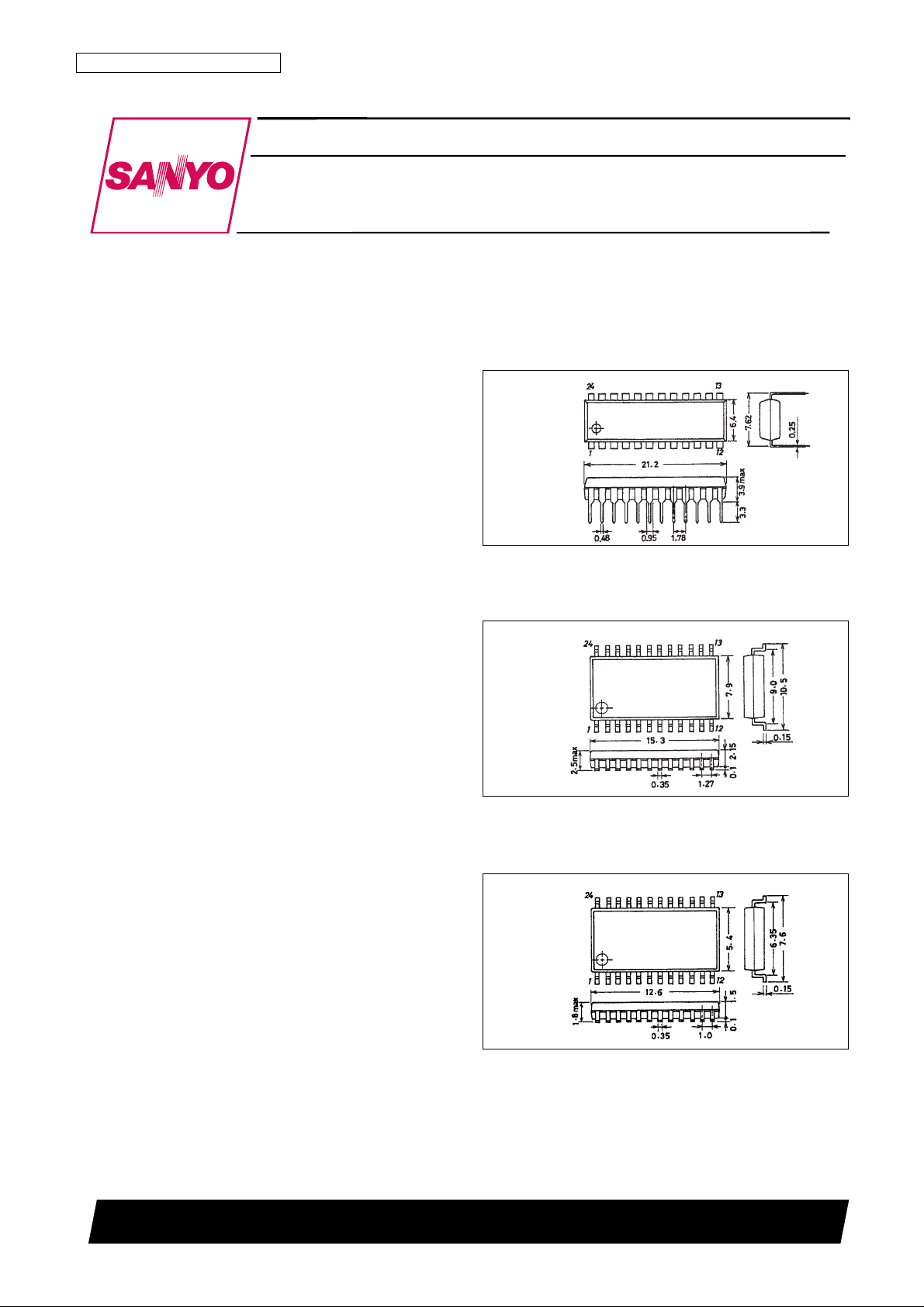
• Package
— 24-pin plastic DIP-24S (300 mil)
— 24-pin plastic MFP-24 (375 mil)
— 24-pin plastic MFP-24S (300 mil)
Package Dimensions
unit: mm
3067-DIP24S
unit: mm
3045B-MFP24
unit: mm
3112-MFP24S
CMOS IC
30698HA (OT) No. 5730-1/23
SANYO: DIP24S
[LC74787]
SANYO: MFP24
[LC74787M]
SANYO: MFP24S
[LC74787JM]
SANYO Electric Co.,Ltd. Semiconductor Bussiness Headquarters
TOKYO OFFICE Tokyo Bldg., 1-10, 1 Chome, Ueno, Taito-ku, TOKYO, 110-8534 JAPAN
On-Screen Display Controller
LC74787, 74787M, 74787JM
Ordering number : EN5730A
Pin Assignment
No. 5730-2/23
LC74787, 74787M, 74787JM
Pin Functions
Pin No. Pin Name Function Notes
1 V
SS
1 Ground Ground connection (digital system ground)
2 Xtal
IN
These pins are used either to connect the crystal and capacitors used to form an external
Crystal oscillator
crystal oscillator circuit to generate the internal synchronizing signals, or to input an external
Xtal
OUT
(MUTE input)
clock signal (2fsc or 4fsc). As a mask option, the XtalOUT pin can be set to function as the
3
(MUTE) MUTE input pin. When this pin is set low, the video output is held at the pedestal level. (A pull-
up resistor is built in and the input has hysteresis characteristics.)
Switches the mode between external clock input and crystal oscillator operation. A low level
4
CTRL1 Crystal oscillator input switching selects crystal oscillator operation and a high level selects external clock input. As a mask
(CHABLK) (CHABLK output) option, the CTRL1 input pin can be set to function as the CHABLK (character · frame) output.
This is a 3-value output.
5 HFTON
OUT
Background line output
Outputs the range signal specified by LNA*, LNB*, and LNC*. Outputs the crystal oscillator
clock when RST is low. (This signal is not output after a reset command is executed.)
6 OSC
IN
LC oscillator
Connections for the inductor and capacitor that form the character output dot clock generation
7 OSC
OUT
oscillator.
Outputs the state of the external synchronizing signal presence/absence judgment. Outputs a
8 SYNC
JDG
External synchronizing signal high level when synchronizing signals are present.
judgment output Outputs the dot clock (LC oscillator) when RST is low. (This signal is not output on command
resets.)
9 CS Enable input
Serial data input circuit enable pin. Serial data input is enabled when a low level is input.
A pull-up resistor is built in. (This input has hysteresis characteristics.)
10 SCLK Clock input
Serial data input circuit clock input.
A pull-up resistor is built in. (This input has hysteresis characteristics.)
11 SIN Data input
Serial data input.
A pull-up resistor is built in. (This input has hysteresis characteristics.)
12 V
DD
2 Power supply Composite video signal level adjustment power supply (analog system power supply)
Continued on next page.
LC74787
LC74787M
LC74787JM
A08680

No. 5730-3/23
LC74787, 74787M, 74787JM
Continued from preceding page.
Pin No. Pin Name Function Notes
13 CV
OUT
Video signal output Composite video signal output
14 V
SS
2 Ground Ground connection (analog system ground)
15 CV
IN
Video signal input Composite video signal input
16 V
DD
1 Power supply Power supply (+5 V: digital system power supply)
Video signal input to the internal sync separator circuit (Used as either the horizontal
17 SYN
IN
Sync separator circuit input synchronizing signal or the composite synchronizing signal input when the internal sync
separator circuit is not used.)
18 SEPC
Sync separator circuit bias
Internal sync separator circuit bias voltage monitor
voltage
19 SEP
OUT
Composite synchronizing Internal sync separator circuit composite synchronizing signal output. Can be switched to
signal output function as a signal (high, low, or ST. pulse) output by the SEL0 and MOD0 setting.
Inputs the vertical synchronizing signal created by integrating the SEP
OUT
pin output signal.
20 SEP
IN
Vertical synchronizing signal input
An integration circuit must be connected to the SEP
OUT
pin. This pin must be tied to VDD1 if
unused. This pin can be switched to function as the frame signal input mode by setting SEL1
high. This is valid when CTL3 is set high. This input has hysteresis characteristics.
Pin settings take priority for switching between the NTSC, PAL, PAL-M, PAL-N, NTSC 4.43,
21 CTRL2 NTSC/PAL-M selection input
and PAL60 video formats. The NTSC format is selected when this pin is low after a reset.
The command video format (NTSC, PAL, PAL-M, PAL-N, NTSC 4.43, or PAL60) selection is
valid. The PAL-M format is selected when this pin is high.
22 CDLR
Background color phase
Background color phase adjustment. Connect a resistor between this pin and ground.
adjustment
23 RST Reset input
System reset input.
A pull-up resistor is built in and the input has hysteresis characteristics.
24 V
DD
1 Power supply (+5 V) Power supply (+5 V: digital system power supply)
Note: Both VDD1 pins must be connected to the power supply.
No. 5730-4/23
LC74787, 74787M, 74787JM
Parameter Symbol Conditions Ratings Unit
Maximum supply voltage V
DD
max VDD1 and VDD2 VSS–0.3 to VSS+6.5 V
Maximum input voltage V
IN
max All input pins VSS–0.3 to VDD+0.3 V
Maximum output voltage V
OUT
max HFTON
OUT
, SYNC
JDG
, and SEP
OUT
VSS–0.3 to VDD+0.3 V
Allowable power dissipation Pd max Ta = 25°C 350 mW
Operating temperature Topr –30 to +70 °C
Storage temperature Tstg –40 to +125 °C
Specifications
Absolute Maximum Ratings
Parameter Symbol Conditions
Ratings
Unit
min typ max
Supply voltage
V
DD
1 VDD1 4.5 5.0 5.5 V
V
DD
2 VDD2 4.5 5.0 1.27 VDD1 V
Input high-level voltage
V
IH
1 RST, CS, SIN, SCLK, SEPIN, and MUTE 0.8 VDD1 VDD1+0.3 V
V
IH
2 CTRL1 and CTRL2 0.7 VDD1 VDD1+0.3 V
Input low-level voltage
V
IL
1 RST, CS, SIN, SCLK, SEPIN, and MUTE V
SS
– 0.3 0.2 VDD1 V
V
IL
2 CTRL1 and CTRL2 V
SS
– 0.3 0.3 VDD1 V
Pull-up resistance R
PU
RST, CS, SIN, SCLK, and MUTE
25 50 90 kΩ
Applies to pins set up by options.
Composite video signal input voltage
V
IN
1 CVIN: VDD1 = 5 V 2.0 Vp-p
V
IN
2 SYNIN: VDD1 = 5 V 2.0 2.5 Vp-p
Input voltage V
IN
3
Xtal
IN
(when used for external clock input)
0.10 5.0 Vp-p
f
IN
= 2fsc or 4fsc ; VDD1 = 5 V
Xtal
IN
and Xtal
OUT
oscillator pins (2fsc: NTSC) 7.159 MHz
Xtal
IN
and Xtal
OUT
oscillator pins (4fsc: NTSC) 14.318 MHz
Xtal
IN
and Xtal
OUT
oscillator pins (2fsc: PAL) 8.867 MHz
F
OSC
1
Xtal
IN
and Xtal
OUT
oscillator pins (4fsc: PAL) 17.734 MHz
Oscillator frequencies Xtal
IN
and Xtal
OUT
oscillator pins (2fsc: PAL-M) 7.151 MHz
Xtal
IN
and Xtal
OUT
oscillator pins (4fsc: PAL-M) 14.302 MHz
Xtal
IN
and Xtal
OUT
oscillator pins (2fsc: PAL-N) 7.164 MHz
Xtal
IN
and Xtal
OUT
oscillator pins (4fsc: PAL-N) 14.328 MHz
F
OSC
2 OSCINand OSC
OUT
oscillator pins (LC oscillator) 5 10 MHz
Allowable Operating Ranges
Note: Applications must be especially cautious about noise when using the XtalINinput pin in clock input mode.
No. 5730-5/23
LC74787, 74787M, 74787JM
Parameter Symbol Pin Conditions
Ratings
Unit
min typ max
Input off leakage current I
leak1
CV
IN
1 µA
Output off leakage current I
leak2
CV
OUT
1 µA
Output high-level voltage V
OH1
HFTON
OUT
, SYNC
JDG
, and SEP
OUT
VDD1 = 4.5 V,
3.5 V
I
OH
= –1.0 mA
Output low-level voltage V
OL
1 HFTON
OUT
, SYNC
JDG
, and SEP
OUT
VDD1 = 4.5 V,
1.0 V
I
OL
= –1.0 mA
H 3.3 5.0 V
Three-value output voltage V
O
CHABLK VDD1 = 5.0 V M 1.8 2.3 V
L 0 0.8 V
Input current
I
IH
RST, CS, SIN, SCLK, CTRL1,
V
IN
= VDD1 1 µA
SEP
IN
, and MUTE
I
IL
CTRL1 and OSC
IN
VIN= VSS1 –1 µA
All outputs: open
Operating mode current drain
I
DD
1 VDD1
Xtal:7.159 MHz
15 mA
LC:8 MHz
I
DD
2 VDD2 VDD2 = 5 V 20 mA
(1) 0.70 0.82 0.94
SYNC level V
SN
(2) 0.89 1.01 1.13 V
(3) 1.18 1.30 1.42
(1) 1.32 1.44 1.56
Pedestal level V
PD
(2) 1.52 1.64 1.76 V
(3) 1.81 1.93 2.05
(1) 0.98 1.10 1.22
Color burst low level V
CBL
(2) 1.17 1.29 1.41 V
(3) 1.46 1.58 1.70
(1) 1.63 1.75 1.87
Color burst high level V
CBH
(2) 1.83 1.95 2.07 V
(3) 2.11 2.23 2.35
(1) 1.17 1.29 1.41
Background color low level (other than blue) V
RSL
0 (2) 1.36 1.48 1.60 V
(3) 1.65 1.77 1.89
(1) 2.33 2.45 2.57
Background color high level (other than blue) V
RSH
0 CV
OUT
(2) 2.52 2.64 2.76 V
(1): When the sync level = 0.8 V V
DD
1 = 5.0 V (3) 2.81 2.93 3.05
(2): When the sync level = 1.0 V V
DD
2 = 5.0 V (1) 1.08 1.20 1.32
Blue background 1 low level V
RSL
1 (3): When the sync level = 1.3 V (2) 1.27 1.39 1.51 V
(3) 1.56 1.68 1.80
(1) 1.49 1.61 1.83
Blue background 2 low level V
RSL
2 (2) 1.68 1.80 1.92 V
(3) 1.97 2.09 2.21
(1) 1.97 2.09 2.21
Blue background 1 and 2 high level V
RSH
1, 2 (2) 2.17 2.29 2.41 V
(3) 2.46 2.58 2.70
(1) 1.40 1.52 1.64
Frame level 0 V
BK
0 (2) 1.60 1.72 1.84 V
(3) 1.89 2.01 2.13
(1) 1.97 2.09 2.21
Frame level 1 V
BK
1 (2) 2.17 2.29 2.41 V
(3) 2.46 2.58 2.70
(1) 2.55 2.67 2.79
Character level V
CHA
(2) 2.75 2.87 2.99 V
(3) 3.04 3.16 3.28
Electrical Characteristics at Ta = –30 to +70°C. VDD1 = 5 V unless otherwise specified.
Note: Blue background 1 or 2 are option settings.
No. 5730-6/23
LC74787, 74787M, 74787JM
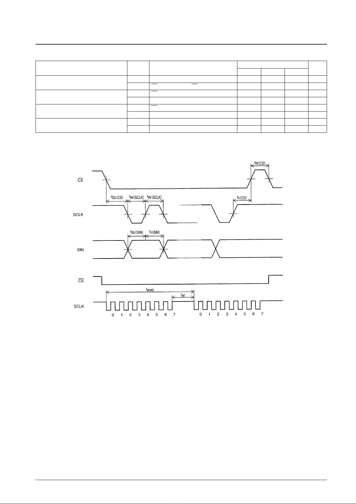
Parameter Symbol Conditions
Ratings
Unit
min typ max
Minimum input pulse width
t
W(SCLK)
SCLK 200 ns
t
W(CS)
CS (The period when CS is high) 1 µs
Data setup time
t
SU(CS)
CS 200 ns
t
SU(SIN)
SIN 200 ns
Data hold time
t
h(CS)
CS 2 µs
t
h(SIN)
SIN 200 ns
One word write time
t
word
The time to write 8 bits of data 4.2 µs
t
wt
The RAM data write time 1 µs
Timing Characteristics at Ta = –30 to +70°C, VDD1 = 5 ±0.5 V
Serial Data Input Timing
First byte
Second byte
A08681
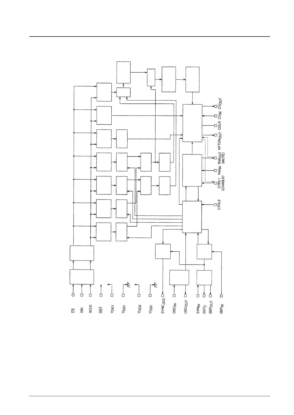
System Block Diagram
No. 5730-7/23
LC74787, 74787M, 74787JM
Serial to
parallel
converter
8-bit
latch +
command
decode
Horizontal
character
size register
Vertical
character
size register
Horizontal
display
position
register
Vertical
display
position
register
Blinking and
reverse
control
register
Display
control
register
RAM write
address
counter
Display
RAM
Deco-
der
Decoder
Font ROM
Shift register
Character output
control
Background control
Video output control
Blinking and
reverse
control circuit
Vertical dot
counter
Horizontal
dot counter
Vertical size
counter
Horizontal
size counter
Vertical display
position
detector
Horizontal
display position
detector
Line control
counter
Character
control
counter
Synchroni-
zation
determination
Composite sync
signal separation
control
Sync
separator
Character
output dot
clock
generator
Sync signal
generator
Timing generator
A08682
 Loading...