

SANYO LC73701M Datasheet
CMOS LSI
No. 5561
Overview
The LC73701M is a DTMP/pulse output dual-system
dialer CMOS LSI for use in push-button telephones. It
provides an on-chip serial interface and operates under the
control of data sent over that serial interface. The
LC73701M can be easily controlled by the system CPU
using this dedicated interface.
Functions
• Functions as a dialer that is controlled over a serial
interface.
• The built-in oscillator circuit (f
either a crystal oscillator or a ceramic resonator as its
oscillator element.
• The adoption of a high-precision (±0.04%) DTMF
signal frequency divider circuit allows a ceramic
resonator to be used as the oscillator element.
• The buffer memory can store up to 32 digits of 5-bit
data.
• Mode change and pause commands can also be stored as
data in the buffer memory.
• Pauses can be inserted automatically on mode changes
(auto-pause).
• A pause can be cancelled during that pause.
• The mode change function supports changing from pulse
to tone (single direction).
• Generates all 16 DTMF signals.
• The pulse dialer output can be turned on or off
arbitrarily.
• The pulse dialer output circuit can be selected to be
either an n-channel open drain or a complementary
circuit.
• The pulse dialer muting function can be turned on or off
arbitrarily.
• A redial function is provided.
• Flash operation is supported. (Data can be received
during flash operation.)
• The flash time can be switched to be either 277 or 707
ms.
• The pause time can be switched to be either 2 or 4
seconds.
• Hooking pause operation is supported. (1.2 s or 801 ms)
• The dial pulse rate can be specified to be either 10 pps
or 20 pps.
= 4.19 MHz) can use
OSC
LC73701M
Serial Interface Dialler
• The dial pulse make ratio can be specified to be either
33 or 39%.
• Wide operating voltage range
Pulse mode: VDD= 1.5 to 5.5 V
DTMF mode: V
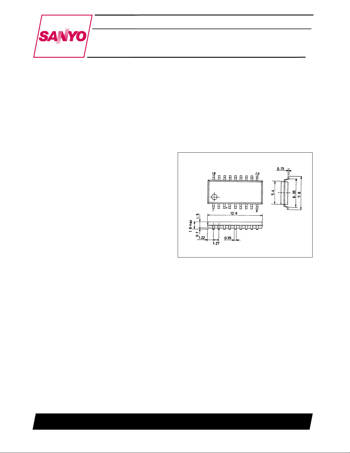
Package Dimensions
unit: mm
3095-MFP18
[LC73701M]
= 2.0 to 5.5 V
DD
SANYO: MFP18
SANYO Electric Co.,Ltd. Semiconductor Bussiness Headquarters
TOKYO OFFICE Tokyo Bldg., 1-10, 1 Chome, Ueno, Taito-ku, TOKYO, 110 JAPAN
53197HA(OT) No. 5561-1/11
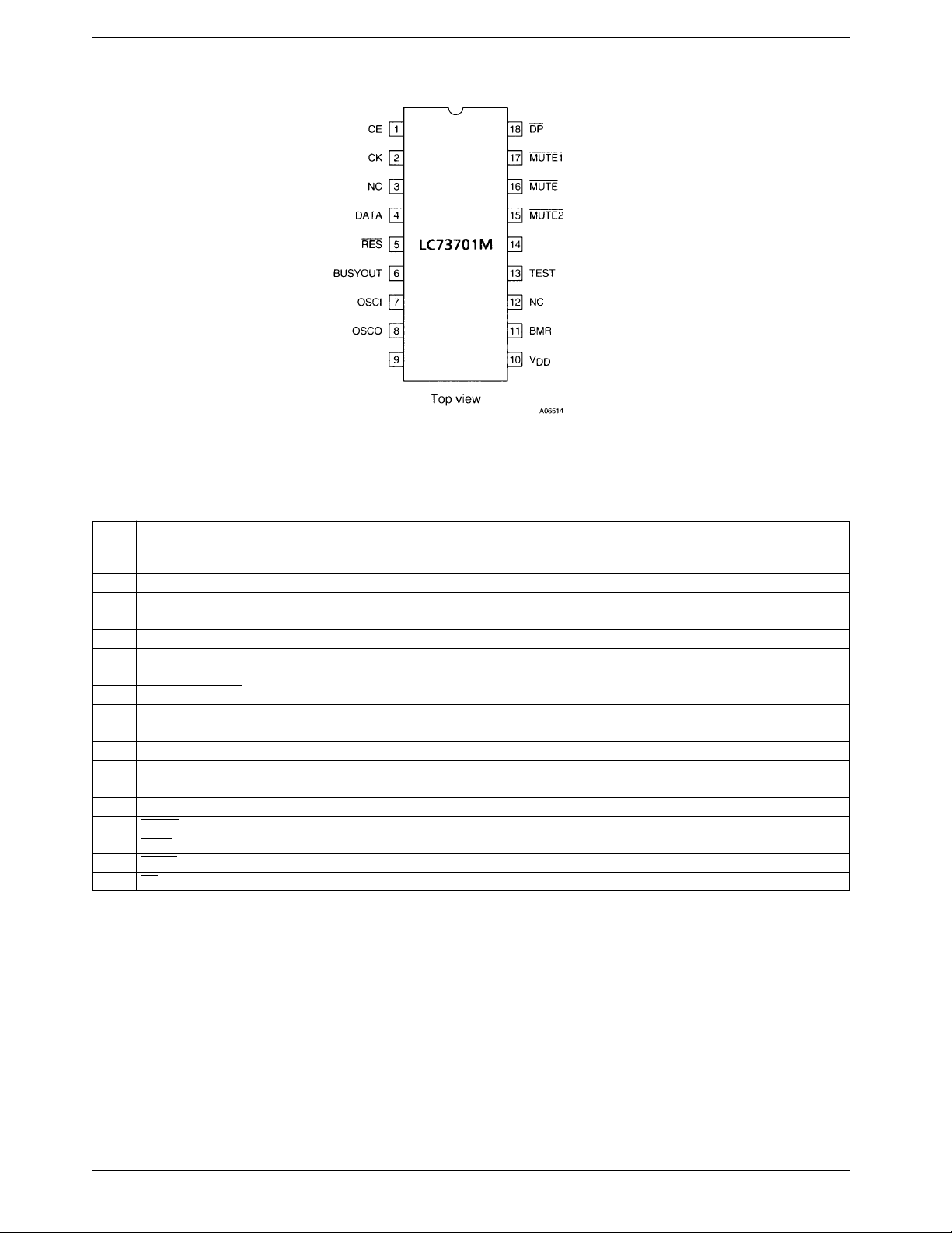
Pin Assignment
LC73701M
DTMF
V
SS
Pin Functions
Pin No. Pin I/O Pin function
1 CE I Set high when data is valid. This signal is also used when DTMF signals are issued consecutively in DTMF mode. The last
2 CK I Data acquisition clock. Data is acquired on the rising edge of this signal.
3NC
4 DATA I Input for the 8-bit data.
5 RES I Reset input. Apply a low level to this input to reset dialer operation when, for example, power is first applied.
6 BUSYOUT O Outputs a high level during dialer operation, including during pauses. This is a complementary output.
7 OSCI I
8 OSCO O
9V
SS
10 V
DD
11 BMR I Make ratio switching input. High: 33%, Low: 39%
12 NC
13 TEST I LSI internal test pin. This pin either must be left open or must be tied low during normal operation.
14 DTMF O DTMF output. This is an npn emitter-follower output.
15 MUTE2 O DTMF mute output. This is an n-channel open-drain output.
16 MUTE O DP and DTMF mute output. This is an n-channel open-drain output.
17 MUTE1 O DP mute output. This is an n-channel open-drain output.
18 DP O DP output. This can be either an n-channel open-drain output or a complementary output.
Unused inputs must always be tied to an appropriate logic level, i.e. either ground or VDD.
DTMF signal is output until CE goes low.
Oscillator circuit connections. Connect either a crystal or ceramic 4.194304 MHz oscillator element to these pins.
Power supply
No. 5561-2/11
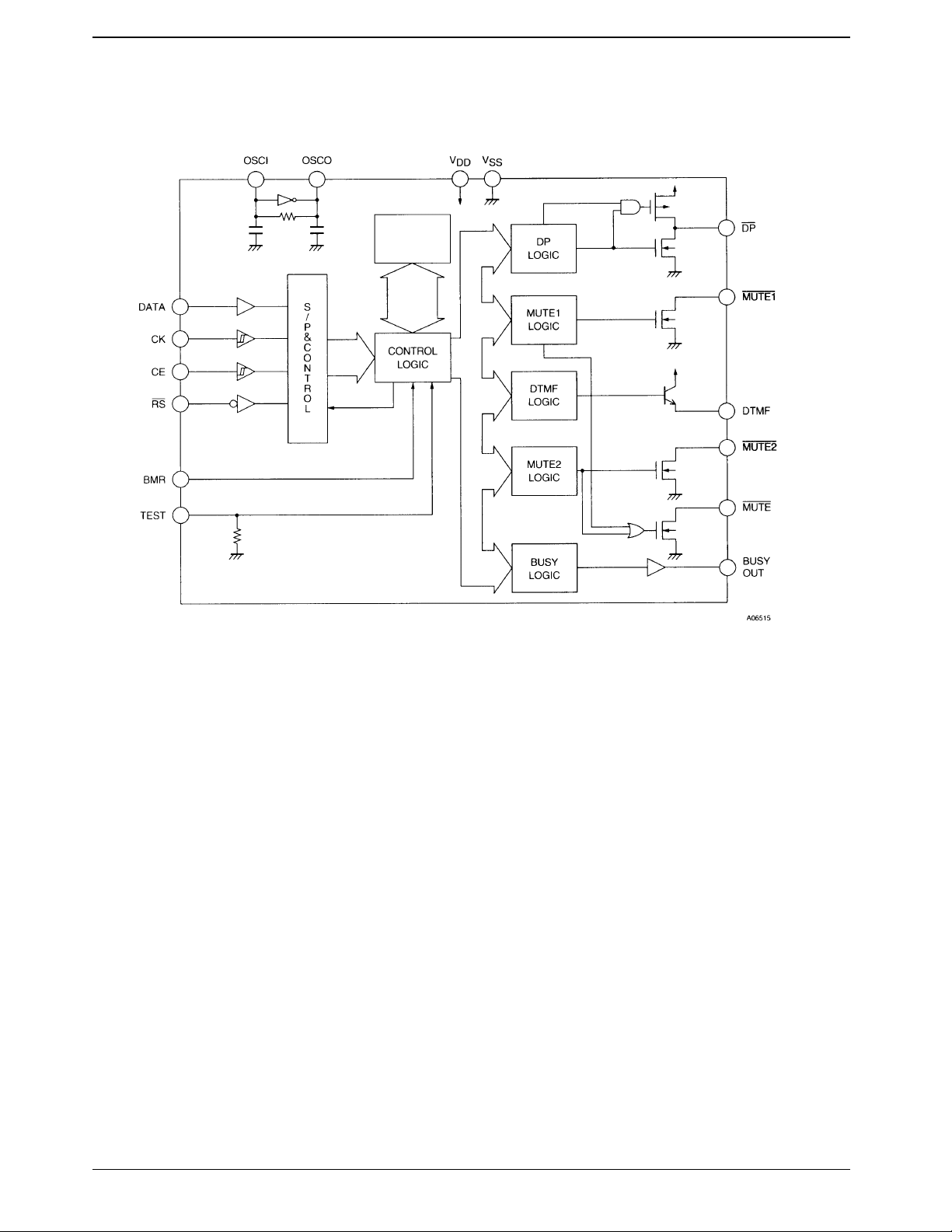
Block Diagram
LC73701M
RAM
5 bits × 32 digits
No. 5561-3/11

Input Code Table
LC73701M
D7 D6 D5 D4 D3 D2 D1 D0
X 0 0 0 0 0 0 0 YES KEY D
X 0 0 0 0 0 0 1 YES KEY 1
X 0 0 0 0 0 1 0 YES KEY 2
X 0 0 0 0 0 1 1 YES KEY 3
X 0 0 0 0 1 0 0 YES KEY 4
X 0 0 0 0 1 0 1 YES KEY 5
X 0 0 0 0 1 1 0 YES KEY 6
X 0 0 0 0 1 1 1 YES KEY 7
X 0 0 0 1 0 0 0 YES KEY 8
X 0 0 0 1 0 0 1 YES KEY 9
X 0 0 0 1 0 1 0 YES KEY 0
X 0 0 0 1 0 1 1 YES KEY *
X 0 0 0 1 1 0 0 YES KEY #
X 0 0 0 1 1 0 1 YES KEY A
X 0 0 0 1 1 1 0 YES KEY B
X 0 0 0 1 1 1 1 YES KEY C
X 0 0 1 0 0 0 0 NO Illegal value
X 0 0 1 0 0 0 1 NO Illegal value
X 0 0 1 0 0 1 0 NO PAUSE clear (Only valid during a pause.)
X 0 0 1 0 0 1 1 NO FLASH (707 or 277 ms)
X 0 0 1 0 1 0 0 NO STOP (Forced termination of a the current dialing operation.)
X 0 0 1 0 1 0 1 NO RD (redial)
X 0 0 1 0 1 1 0 NO MUTE ST
X 0 0 1 0 1 1 1 NO MUTE END
X 0 0 1 1 0 0 0 NO ON-HOOK
X 0 0 1 1 0 0 1 NO OFF-HOOK
X 0 0 1 1 1 0 0 YES MODE-CH (Pulse to tone single-direction change)
X 0 0 1 1 1 0 1 YES PAUSE (Pause for either 2.0 or 4.0 seconds.)
WRITE
TO RAM
Data interpretation and notes
X : Don’t care
Only bits D0 to D4 are written to RAM.
Mode Settings Command Table
D7 D6 D5 D4 D3 D2 D1 D0
X MODE TEST DPSEL PAUSE FLASH P/T DPR
X (1) (0) (0) N-CH OD (0) 4.0 s (0) 707.0 ms (0) Tone (0) 20 pps
X (1) (0) (0) CMP (1) 2.0 s (1) 277.3 ms (1) Pulse (1) 10 pps
Flash time Hooking pause time
707.0 ms..................800.8 ms
277.3 ms..................1.23 s
Note that a hooking pause of 804.7 ms is also inserted automatically on a DP-off operation.
No. 5561-4/11
 Loading...