

SANYO LC36256AMLL-70, LC36256AMLL-12, LC36256ALL-85, LC36256ALL-70, LC36256ALL-12 Datasheet
...
Ordering number : EN4327A
32896HA (OT)/21593JN (OT) No. 4327-1/7
Overview
The LC36256ALL, AMLL are fully asynchronous silicon
gate CMOS static RAMs with a 32768 words × 8 bits
configuration.
This series has CE chip enable pin for device
select/nonselect control and an OE output enable pin for
output control, and features high speed as well as low
power dissipation.
Current dissipation is notably reduced during stand-by and
data retention. For these reasons, this series is most suited
for use in systems requiring high speed, low power
consumption and long-term battery backup. Simple
memory capacity expansion is also supported.
Features
• Access time
70 ns (max.) :
LC36256ALL-70, LC36256AMLL-70
85 ns (max.) :
LC36256ALL-85, LC36256AMLL-85
100 ns (max.) :
LC36256ALL-10, LC36256AMLL-10
120 ns (max.) :
LC36256ALL-12, LC36256AMLL-12
• Low current dissipation
During standby
0.5 µA (max.) / Ta = 25°C
1 µA (max.) / Ta = 0 to +40°C
5 µA (max.) / Ta = 0 to +70°C
During data retention
0.3 µA (max.) / Ta = 25°C
0.6 µA (max.) / Ta = 0 to +40°C
3 µA (max.) / Ta = 0 to +70°C
During operation (DC)
10 mA (max.)
• Single 5 V power supply: 5 V ±10%
• Data retention power supply voltage: 2.0 to 5.5 V
• No clock required (Fully static memory)
• All input/output levels are TTL compatible
• Common input/output pins, with three output states
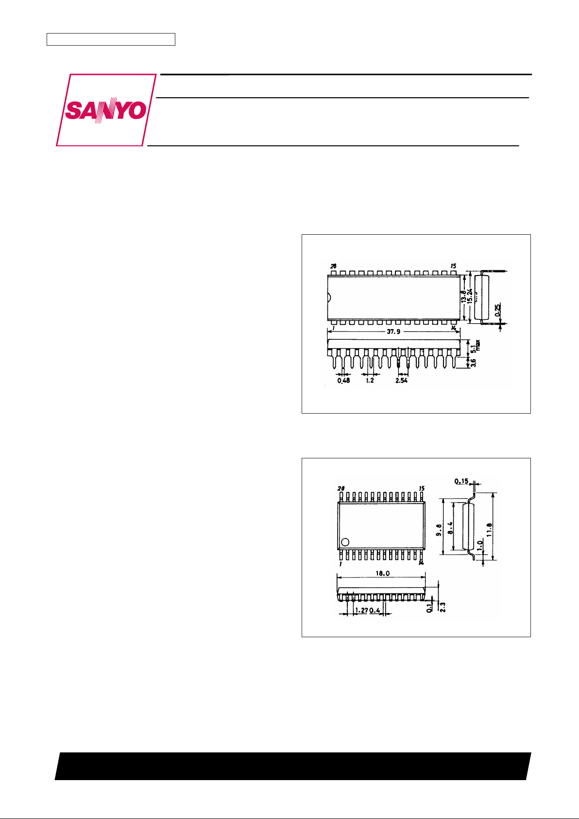
• Packages
DIP 28- pin (600 mil) plastic package : LC36256ALL
SOP 28-pin (450 mil) plastic package :
LC36256AMLL
Package Dimensions
unit: mm
3012A-DIP28
unit: mm
3187-SOP28D
SANYO: DIP28
[LC36256ALL]
SANYO: SOP28D
[LC36256AMLL]
LC36256ALL, AMLL-70/85/10/12
SANYO Electric Co.,Ltd. Semiconductor Bussiness Headquarters
TOKYO OFFICE Tokyo Bldg., 1-10, 1 Chome, Ueno, Taito-ku, TOKYO, 110-0005 JAPAN
256 K (32768 words × 8 bits) SRAM
Asynchronous Silicon Gate CMOS LSI
LC36256ALL, AMLL-70/85/10/12
No. 4327-2/7
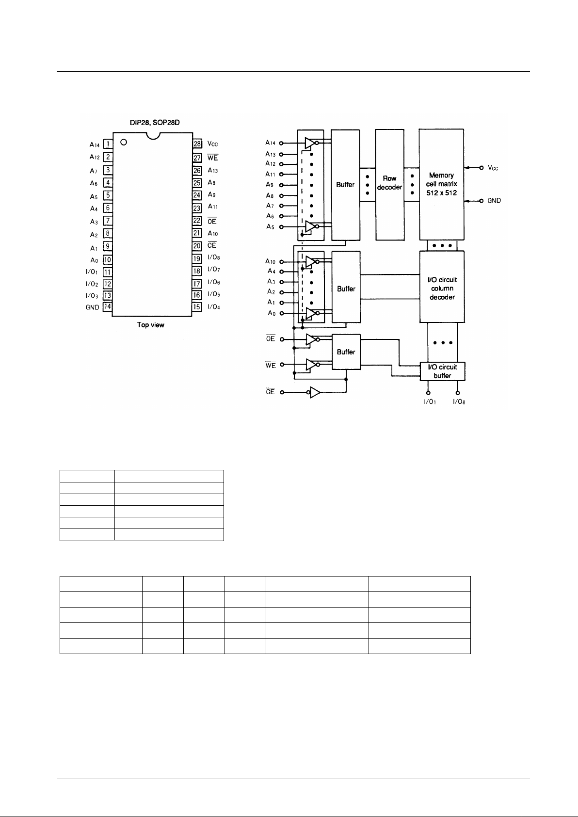
Pin Assignment Block Diagram
Functions
Mode CE OE WE I/O Supply current
Read cycle L L H Data output I
CCA
Write cycle L X L Data input I
CCA
Output disable L H H High impedance I
CCA
Nonselect H X X High impedance I
CCS
X : H or L
Pin Functions
A0 to A14 Address input
WE Read/write control input
OE Output enable input
CE Chip enable input
I/O1 to I/O8 Data input/output
VCC, GND Power supply pins
Specifications
Absolute Maximum Ratings at Ta=25°C
Parameter Symbol Conditions Ratings Unit
Maximum supply voltage V
CC max 7.0 V
Input pin voltage V
IN –0.5* to VCC+0.5 V
I/O pin voltage V
I/O –0.5* to VCC+0.5 V
Allowable power dissipation Pd max
LC36256ALL 1.0 W
LC36256AMLL 0.7 W
Operating temperature range Topr 0 to +70 °C
Storage temperature range Tstg –55 to +150 °C
* –3.0 V when pulse width is less than 50 ns
DC Recommended Operating Ranges at Ta = 0 to +70°C
Parameter Symbol min typ max Unit
Power supply voltage V
CC 4.5* 5.0 5.5 V
Input high level voltage V
IH 2.2* VCC+0.3 V
Input low level voltage V
IL –0.3* +0.8 V
* –3.0 V when pulse width is less than 50 ns
DC Electrical Characteristics at Ta = 0 to +70°C, VCC = 5 V ±10%
Parameter Symbol Conditions min typ* max Unit
Input leakage current I
LI VIN = 0 to VCC –0.5 +0.5 µA
I/O leakage current I
LO VCE = VIH or VOE = VIH, –0.5 +0.5 µA
V
I/O = 0 to VCC
Output high level voltage
VOH IOH = –1.0mA 2.4 V
Output low level voltage VOL IOL = 2.1mA 0.4 V
Operating supply
I
CCA1
VCE ≤ 0.2V, 1 5 mA
current (DC)
V
IN ≤ 0.2V or VIN ≥ VCC–0.2V
I
CCA2 VCE = VIL, II/O=0mA 3 10 mA
min cycle
70ns 30 50
Average operating
I
CCA3 Duty = 100%
85ns 25 50
mA
supply current
I
I/O
= 0mA
100ns 23 50
120ns 20 50
0 to +70°C
5
Standby supply
I
CCS1 V
CE ≥VCC
-0.2V
0 to +40°C
1 µA
current
25°C 0.2 0.5
I
CCS2 VCE = VIH 0.4 2 mA
* Reference values at V
CC = 5 V, Ta = 25°C
LC36256ALL, AMLL-70/85/10/12
No. 4327-3/7
Access
time
 Loading...