

SANYO LC35V256ET Datasheet

Ordering number : ENN6303
12800RM (OT) No. 6303-1/6
Overview
The LC35V256EM-70W and LC35V256ET-70W are
asynchronous silicon-gate CMOS SRAMs with a 32768word by 8-bit structure. These are full-CMOS devices
with 6 transistors per memory cell, and feature ultralowvoltage operation, a low operating current drain, and an
ultralow standby current. Control inputs include OE for
fast memory access and CE for power saving and device
selection. This makes these devices optimal for systems
that require low power or battery backup, and makes
memory expansion easy. The ultralow standby current
allows these devices to be used with capacitor backup as
well.
Features
• Supply voltage range: 3.0 to 3.6 V
• Access time: 70 ns (maximum)
• Standby current: 0.8 µA (Ta ≤ 60°C)
4.0 µA (Ta ≤ 70°C)
• Operating temperature: –10 to +70°C
• Data retention voltage: 2.0 to 3.6 V
• All I/O levels: CMOS compatible (0.8 VCC, 0.2 VCC)
• Input/output shared function pins, 3-state output pins
• No clock required (fully static circuits)
• Package
28-pin SOP (450 mil) plastic package:
LC35V256EM-70W
28-pin TSOP (8 × 13.4 mm) plastic package:
LC35V256ET-70W
Package Dimensions
unit: mm
3187A-SOP28D
unit: mm
3221-TSOP28 (Type I)
LC35V256EM, ET-70W
SANYO Electric Co.,Ltd. Semiconductor Company
TOKYO OFFICE Tokyo Bldg., 1-10, 1 Chome, Ueno, Taito-ku, TOKYO, 110-8534 JAPAN
256K (32K words × 8 bits) SRAM
Control pins: OE and CE
CMOS IC
1
14
15
28
11.8
1.0
8.4
9.8
18.0
0.1
2.3
1.27
0.4
0.15
SANYO: SOP28D
[LC35V256EM-70W]
Any and all SANYO products described or contained herein do not have specifications that can handle
applications that require extremely high levels of reliability, such as life-support systems, aircraft’s
control systems, or other applications whose failure can be reasonably expected to result in serious
physical and/or material damage. Consult with your SANYO representative nearest you before using
any SANYO products described or contained herein in such applications.
SANYO assumes no responsibility for equipment failures that result from using products at values that
exceed, even momentarily, rated values (such as maximum ratings, operating condition ranges, or other
parameters) listed in products specifications of any and all SANYO products described or contained
herein.
0.55
22 7
21 8
1
28
8.1
1.27max
11.8
13.4
0.5
0.2
0.125
0.08
SANYO: TSOP28 (Type I)
[LC35V256ET-70W]
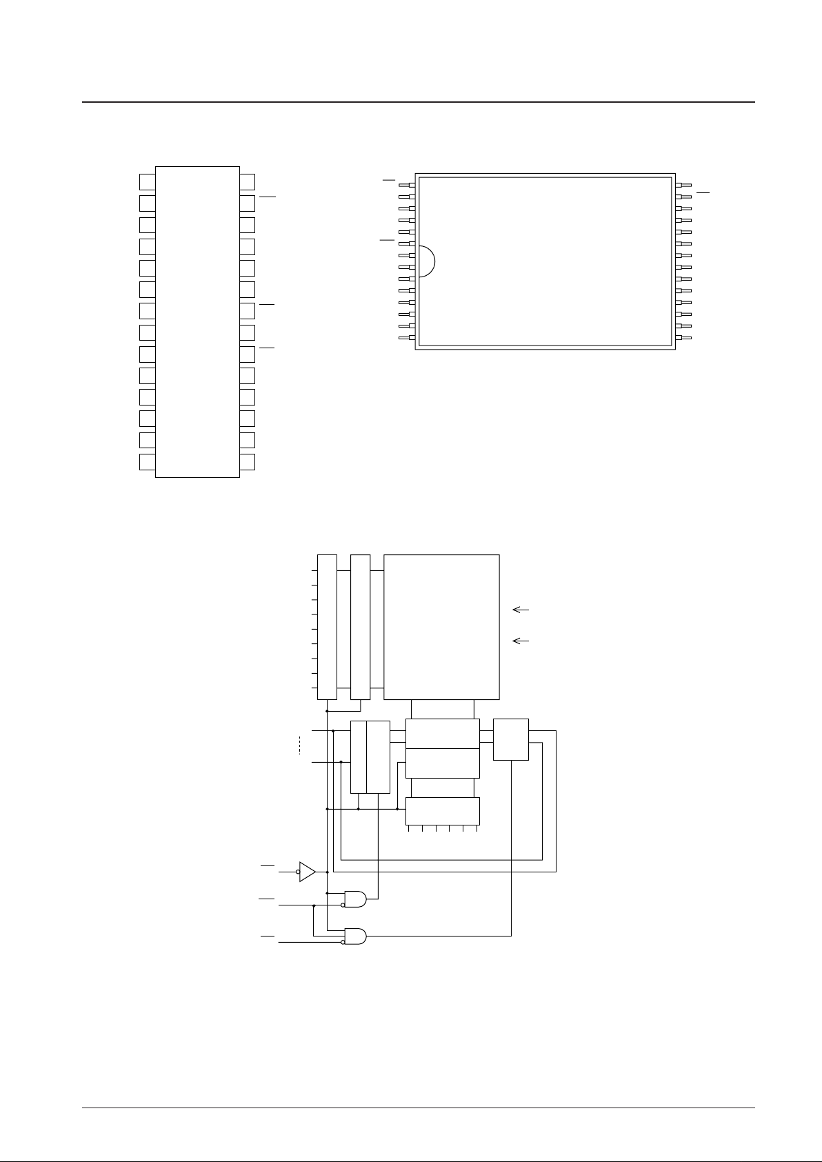
Pin Assignment (Top view)
No. 6303-2/6
LC35V256EM, ET70W
1
2
3
4
5
6
7
8
9
10
11
12
13
14
28
27
26
25
24
23
22
21
20
19
18
17
16
15
A
14
V
CC
WE
A
13
A
8
A
9
A
11
OE
A
10
CE
I/O
8
I/O
7
I/O
6
I/O
5
I/O
4
A
12
A
7
A
6
A
5
A
4
A
3
A
2
A
1
A
0
I/O
1
I/O
2
I/O
3
GND
LC35V256EM-70W
SOP28
OE 22
23
24
25
26
27
28
1
2
3
4
5
6
7
21
20
19
18
17
16
15
14
13
12
11
10
9
8
A
11
A
10
I/O
8
I/O
7
I/O
6
I/O
5
I/O
4
GND
I/O
3
I/O
2
I/O
1
A
0
A
1
A
2
CE
A
9
A
8
A
13
WE
V
CC
A
14
A
12
A
7
A
6
A
5
A
4
A
3
TSOP28
LC35V256ET-70W
Block Diagram
A
6
A
7
A
8
A
9
A
10
A
11
A
12
A
13
A
14
V
CC
GND
I/O
1
I/O
8
CE
WE
OE
A0A1A2A3A4A
5
Address buffer
Row decoder
Memory cell array
512 × 512
Column I/O
circuit
Column decoder
Address buffer
Output
data
buffer
Input data buffer
Input data
control circuit
 Loading...