

SANYO LC11014-241 Datasheet

Ordering number: EN 5578
CMOS LSI
LC11014-241
Computer Image Signal Processing
Full-Color Gray-Scale Processor
Overview
The LC11014-241 is a pseudo gray-scale processor for
TFT-LCD panel displays. It allows TFT-LCD panels with
3, 4, 5 or 6-bit input digital drivers to display the equivalent of 16.7 million colors. It can also be used with XGA
panels in 2-pixel parallel input/output mode.
Features
• Handles 8 bits of input data (256-level gray scale data)
for each of the RGB colors
• Realizes reduced resolution loss (as compared to dithering techniques) by using intra-frame and inter-frame
error diffusion processing
• Incorporates a new full-coloration algorithm, formerly
best done using computers
• Operating mode selection of outputs for 3, 4, 5, or 6-bit
drivers
• Selectable 2-pixel parallel input/output, serial-input parallel-output, and serial input/output operating modes
• 40MHz (parallel input/output), 65 MHz (serial input,
parallel output), or 50MHz (serial input/output) maximum clock frequency
• Can operate independently of the number of displayed
pixels since internal operation is controlled by the horizontal and vertical synchronization signals.
• Power-save function to stop the internal operation processing circuits, and output only the clock, sync signals
and control signals
• Supports 5V input signals at 3.3V supply voltage
Package Dimensions
unit: mm
3214-SQFP144
[LC11014-241]
SANYO Electric Co., Ltd. Semiconductor Business Headquarters
TOKYO OFFICE Tokyo Bldg., 1-10, 1 Chome, Ueno, Taito-ku, TOKYO, 110 JAPAN
61297HA (ID) No. 5578—1/13

Pin Assignment
LC11014-241
Block Diagram
Top view
No. 5578—2/13

Pin Summary
P
P
P
LC11014-241
I Input
O Output
PPower
NC No connection
No. Name I/O
1V
SS
P
2 IOMD0 I2
3 IOMD1 I2
4 TEST0 I1
5 TEST1 I1
6 TEST2 I1
7 TEST3 I1
8 CLKSEL I1
9V
DD
P
10 BD10 O1
11 BD11 O1
12 V
SS
P
13 BD12 O1
14 BD13 O1
15 BD14 O1
16 BD15 O1
17 BD00 O1
18 V
19 V
DD
SS
P
P
20 BD01 O1
21 BD02 O1
22 BD03 O1
23 BD04 O1
24 V
SS
P
25 BD05 O1
26 GD10 O1
27 GD11 O1
28 GD12 O1
29 V
30 V
DD
SS
P
P
31 GD13 O1
32 GD14 O1
33 GD15 O1
34 GD00 O1
35 GD01 O1
36 V
SS
P
No. Name I/O
37 V
DD
P
38 GD02 O1
39 GD03 O1
40 GD04 O1
41 GD05 O1
42 V
43 V
SS
DD
P
P
44 RD10 O1
45 RD11 O1
46 RD12 O1
47 RD13 O1
48 V
49 V
SS
DD
P
P
50 RD14 O1
51 RD15 O1
52 RD00 O1
53 RD01 O1
54 V
55 V
DD
SS
P
P
56 RD02 O1
57 RD03 O1
58 RD04 O1
59 RD05 O1
60 V
61 V
DD
SS
P
P
62 HSYNC O2
63 VSYNC O2
64 HDEN O2
65 V
SS
P
66 CLK O3
67 V
68 V
SS
DD
P
P
69 CLKB O3
70 CTL O1
71 NC NC
72 V
SS
I
I1 TTL-level pull-down input buffer
I2 TTL-level input buffer
O1 2mA output buffer
O
O2 4mA output buffer
O3 4mA 3-state output buffer
No. Name I/O
73 V
DD
P
74 GSPMD0 I2
75 GSPMD1 I2
76 GSPMD2 I2
77 VMD I1
78 SHDEN I2
79 SHSYNC I2
80 SVSYNC I2
81 SCLK I2
82 V
SS
P
83 SCTL I1
84 PWRSV I1
85 BYPASS I1
86 SRD07 I2
87 SRD06 I2
88 SRD05 I2
89 SRD04 I2
90 V
91 V
DD
SS
P
P
92 SRD03 I2
93 SRD02 I2
94 SRD01 I2
95 SRD00 I2
96 SRD17 I2
97 SRD16 I2
98 SRD15 I2
99 SRD14 I2
100 V
SS
P
101 SRD13 I2
102 SRD12 I2
103 SRD11 I2
104 SRD10 I2
105 SGD07 I2
106 SGD06 I2
107 SGD05 I2
108 V
SS
No. Name I/O
109 V
DD
P
110 SGD04 I2
111 SGD03 I2
112 SGD02 I2
113 SGD01 I2
114 SGD00 I2
115 SGD17 I2
116 SGD16 I2
117 SGD15 I2
118 V
SS
P
119 SGD14 I2
120 SGD13 I2
121 SGD12 I2
122 SGD11 I2
123 SGD10 I2
124 SBD07 I2
125 SBD06 I2
126 V
127 V
DD
SS
P
P
128 SBD05 I2
129 SBD04 I2
130 SBD03 I2
131 SBD02 I2
132 SBD01 I2
133 SBD00 I2
134 SBD17 I2
135 V
SS
P
136 SBD16 I2
137 SBD15 I2
138 SBD14 I2
139 SBD13 I2
140 SBD12 I2
141 SBD11 I2
142 SBD10 I2
143 DSIFT I1
144 V
DD
No. 5578—3/13
×
LC11014-241
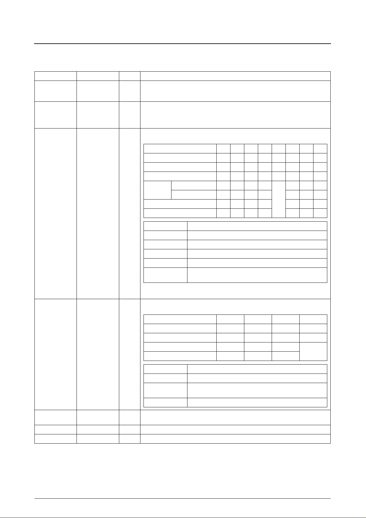
Pin Functions
Symbol Pin No. I/O Function
V
DD
V
SS
GSPMD [0:2] 74 to 76 I
9, 18, 29, 37, 43, 49,
54, 60, 68, 73, 90,
109, 126, 144
1, 12, 19, 24, 30, 36,
42, 48, 55, 61, 65,
67, 72, 82, 91, 100,
108, 118, 127, 135
– Supply voltage (+3.3V)
– Ground (0V)
Mode selection signals [0 to 2] for the gray-scale mode. The setting process for the mode selection lines
is described below. GSPMD0 is the LSB and GSPMD2 is the MSB.
Gray-scale mode 01234567
GSPMD0 LHLHLHLH
GSPMD1 L L H H L L H H
GSPMD2 LLLLHHHH
Processing
Number of valid input bits 8888 888
Number of output bits 3456 456
Intra-frame processing Yes Yes Yes Yes
Inter-frame processing Yes Yes Yes Yes No No No
Yes Yes Yes
Reserved
IOMD [0:1] 2, 3 I
Gray-scale mode LCD module
0 Operating mode for TFT LCD modules with 3-bit source driver
1 Operating mode for TFT LCD modules with 4-bit source driver
2, 6 Operating mode for TFT LCD modules with 5-bit source driver
3, 7 Operating mode for TFT LCD modules with 6-bit source driver
5
Do not use gray-scale modes 0 to 3 with TFT LCD modules that perform FRC or other inter-frame
processing.
Input/output mode select pins. The input/output mode selection lines are described below. IOMD0 is the
LSB and IOMD1 is the MSB.
Input/output mode 0123
Input/output mode LCD module
0 XGA-compatible 2-pixel parallel input interface TFT LCD panels
1
2 Serial input interface VGA and SVGA TFT LCD panels
Operating mode for TFT LCD modules with 3-bit source driver that perform
FRC or other inter-frame processing
IOMD0 LHLH
IOMD1 L L H H
Input Parallel Serial Serial
Output Parallel Parallel Serial
2-pixel parallel input interface TFT LCD panels (serial input is converted to
parallel internally)
Reserved
VMD 77 I
SCLK 81 I Clock signal input. Data is processed according to this clock signal.
DSIFT 143 I In input/output mode 1, data is shifted out on both
Gray-scale processing algorithm select pin. The LC11011-141 algorithm is selected when high. Normal
mode is selected when low or open.
D0 and × D1 when high.
No. 5578—4/13
 Loading...