

SANYO LC11011-141 Datasheet
Overview
The LC11011-141 is a pseudo gray scale processor for
TFT LCD. It allows LCD panels with inputs of three to six
bits per RGB to display the equivalent of 16.7 million
colors.
Features
• Handles 8-bits of input data (256-scale data) for each of
the RGB colors.
• Operating mode selection of three, four, or six bit driver
outputs
• Realizes reduced resolution loss (as compared to
dithering techniques) by using intra- and inter-frame
error diffusion processing.
• Supports both 5 V and low voltage (3.3 V) operation.
• Operates with arbitrary clock frequencies up to 50 MHz
(at 5 V) or up to 30 MHz (at 3.3 V).
• Can operate independently of the number of displayed
pixels since internal operation is controlled by the
horizontal and vertical synchronization signals.
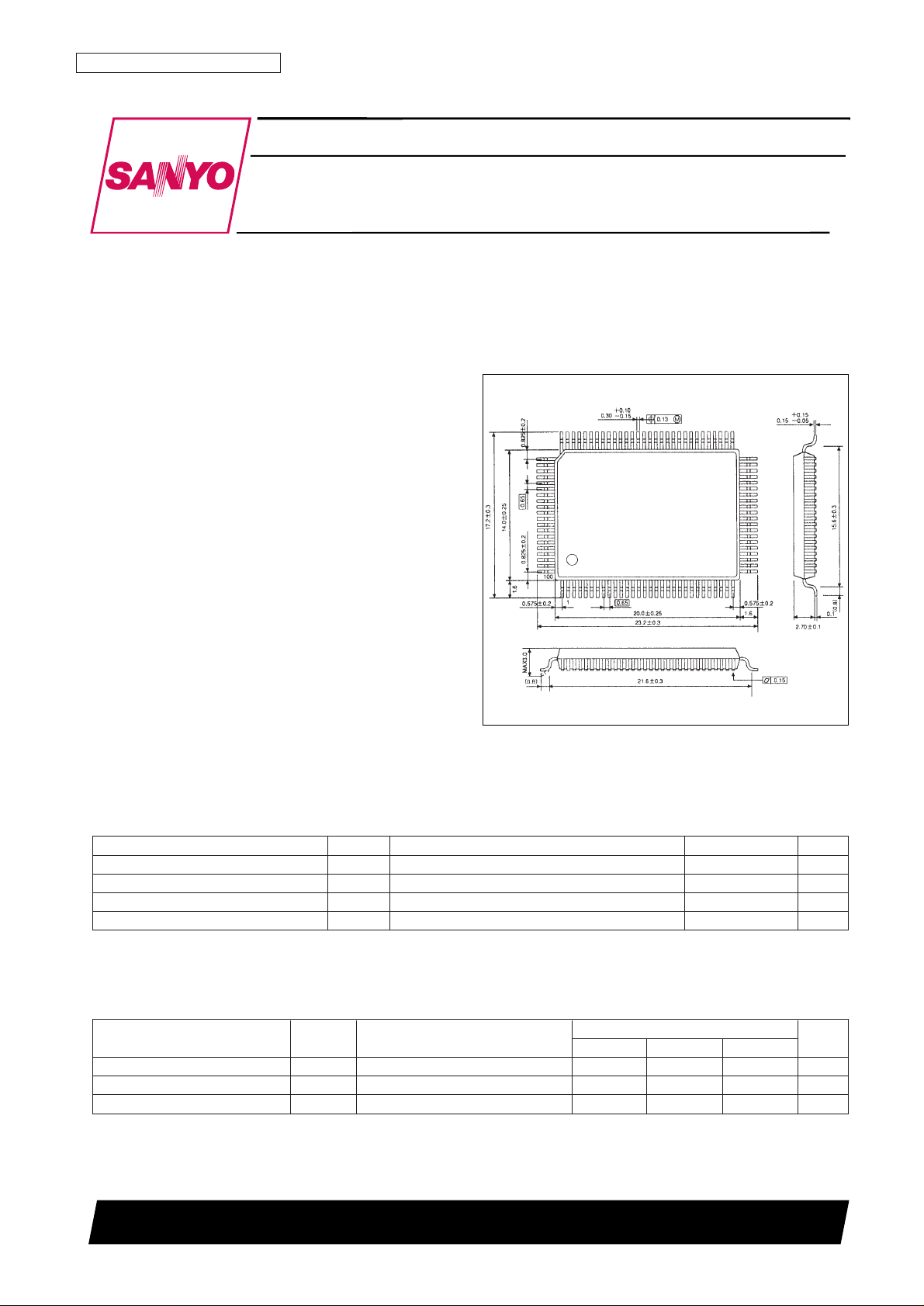
Package Dimensions
unit: mm
3151-QFP100E
CMOS LSI
22896HA (OT)/No. 5041-1/7
Preliminaly
SANYO: QFP100E
[LC11011-141]
SANYO Electric Co.,Ltd. Semiconductor Bussiness Headquarters
TOKYO OFFICE Tokyo Bldg., 1-10, 1 Chome, Ueno, Taito-ku, TOKYO, 110 JAPAN
Computer Image Signal Processing
Full-Color Gray-Scale Processor
LC11011-141
Ordering number : EN*5041A
Specifications
Absolute Maximum Ratings at Ta = 25°C, VSS= 0 V
Electrical Characteristics: At an operating voltage of 5.0 V
Operating Ranges at Ta = 0 to +70°C
Parameter Symbol Conditions Ratings Unit
Maximum supply voltage V
DD
max –0.3 to +7.0 V
Input and output voltages V
I
, V
O
–0.3 to VDD+ 0.3 V
Operating temperature Topr 0 to +70 °C
Storage temperature Tstg –40 to +125 °C
Parameter Symbol Conditions
Ratings
Unit
min typ max
Supply voltage V
DD
4.5 5.0 5.5 V
Input voltage V
IN
0V
DD
V
Clock frequency f
clk
50 MHz

No. 5041-2/7
LC11011-141
DC Characteristics at Ta = 0 to +70°C, VSS= 0 V, VDD= 4.5 to 5.5 V
Note: * The test conditions are: fCP= 25.175 MHz, VDD= 5.0 V, CL= 15 pF (measured with VGA timing)
Switching Characteristics at Ta = 0 to +70°C, VSS= 0 V, VDD= 4.5 to 5.5 V, CL= 15 pF
Electrical Characteristics: At an operating voltage of 3.3 V
Operating Ranges at Ta = 0 to +70°C
DC Characteristics at Ta = 0 to +70°C, V
SS
= 0 V, VDD= 3.0 to 3.6 V
Note: * The test conditions are: f
clk
= 25.175 MHz, VDD= 3.3 V, CL= 15 pF (measured with VGA timing)
Parameter Symbol Conditions
Ratings
Unit
min typ max
High level input voltage V
IH
CMOS level 0.7 V
DD
V
Low level input voltage V
IL
CMOS level 0.3 V
DD
V
High level output voltage V
OH
IOH(–4 mA) 2.4 V
Low level output voltage V
OL
IOL(4 mA) 0.4 V
Supply current I
CC
* 40 70 mA
Parameter Symbol Conditions
Ratings
Unit
min typ max
High level input voltage V
IH
CMOS level 0.7 V
DD
V
Low level input voltage V
IL
CMOS level 0.3 V
DD
V
High level output voltage V
OH
IOH(–2 mA) 2.2 V
Low level output voltage V
OL
IOL(2 mA) 0.4 V
Supply current I
CC
* 30 45 mA
Parameter Symbol Conditions
Ratings
Unit
min typ max
Dot clock cycle time Tdclk 20 ns
Hsync low level pulse width Thpw 2 Tdclk ns
Vsync low level pulse width Tvpw 2 Tdclk ns
Data setup time Tdsu 5 ns
Data hold time Tdhd 5 ns
Control signal setup time Tcsu 5 ns
Control signal hold time Tchd 5 ns
CLK propagation delay time Ttdhh 2 3 6 ns
CLK propagation delay time Ttdll 2 4 7 ns
CLKB propagation delay time Ttdhl 2 4 7 ns
CLKB propagation delay time Ttdlh 2 4 7 ns
Control signal propagation delay time Ttctl 2 Tdclk + 3 2 Tdclk + 6 2 Tdclk + 10 ns
Data output propagation delay time Ttdata 2 Tdclk + 3 2 Tdclk + 6 2 Tdclk + 11 ns
Parameter Symbol Conditions
Ratings
Unit
min typ max
Supply voltage V
DD
3.0 3.3 3.6 V
Input voltage V
IN
0 V
DD
V
Clock frequency f
clk
30 MHz

No. 5041-3/7
LC11011-141
Switching Characteristics at Ta = 0 to +70°C, VSS= 0 V, VDD= 3.0 to 3.6 V, CL= 15 pF
Pin Assignment
Parameter Symbol Conditions
Ratings
Unit
min typ max
Dot clock cycle time Tdclk 33 ns
Hsync low level pulse width Thpw 2 Tdclk ns
Vsync low level pulse width Tvpw 2 Tdclk ns
Data setup time Tdsu 10 ns
Data hold time Tdhd 10 ns
Control signal setup time Tcsu 10 ns
Control signal hold time Tchd 10 ns
CLK propagation delay time Ttdhh 2 5 12 ns
CLK propagation delay time Ttdll 2 6 14 ns
CLKB propagation delay time Ttdhl 2 6 14 ns
CLKB propagation delay time Ttdlh 2 6 14 ns
Control signal propagation delay time Ttctl 2 Tdclk + 5 2 Tdclk + 10 2 Tdclk + 22 ns
Data output propagation delay time Ttdata 2 Tdclk + 5 2 Tdclk + 10 2 Tdclk + 24 ns
 Loading...