

Page 1

Any and all SANYO products described or contained herein do not have specifications that can handle
applications that require extremely high levels of reliability, such as life-support systems, aircraft’s
control systems, or other applications whose failure can be reasonably expected to result in serious
physical and/or material damage. Consult with your SANYO representative nearest you before using
any SANYO products described or contained herein in such applications.
SANYO assumes no responsibility for equipment failures that result from using products at values that
exceed, even momentarily, rated values (such as maximum ratings, operating condition ranges, or other
parameters) listed in products specifications of any and all SANYO products described or contained
herein.
Overview
The LB8632V is a general-purpose camera motor driver
IC that supports low-saturation output and low-voltage
drive and thus can be used in a wide range of applications.
The LB8632V is a miniature thin form-factor IC that
provides circuit structures and I/O logic that reduce
development times and costs and support reduced lot sizes
and end product diversity, despite increasing
miniaturization and functionality in application products.
Since the LB8632V supports low-voltage operation
(starting from 1.2 V) in addition to low-saturation outputs,
it provides characteristics that can withstand operation in
low-voltage ranges even in 3 V popularly-priced cameras
that do not include a step-up circuit. Since the LB8632V
supports IIL, control logic can be optimized by using two
ICs in parallel, thus allowing even more actuators to be
driven with a small number of CPU output ports. Thus the
LB8632V can also be used in 6 V top-of-the-line end
products.
Features
• 3, 6 V and a wide application range: from popularly
priced models to top-of-the-line products
The external transistors and the number of ICs (one or
two) is determined by the number of IC required motors
and actuators.
Support for motor standby, forward, reverse and braking
control for four motors using only five CPU port lines.
This requires two external transistors and two ICs. The
LB8632V also provides non-operating mode logic for
the operating control signals (the IN input) so that ICs
with other functions can be used on the same ports.
• Built-in 1 CH low-voltage drive low-saturation,
forward/reverse motor drive
IOpeak = 3.0 A maximum (t ≤ 100 ms: single shot,
between OUT1 and OUT2)
IODC = 1.0 A maximum
VOsat = 0.45 V typical (at IO= 1 A)
Operating voltage range: VB= 1.2 to 7.5 V (VB= VS=
VDD= battery voltage)
• Built-in low-voltage drive - 0.5 CH forward/reverse
motor driver
Supports 1.5 CH bridge operation with the use of two
external transistors. Also supports LED or solenoid
drive with constant-current drive.
Operating voltage range: VB= 1.2 to 7.5 V (VB= VS=
VDD= battery voltage)
• Built-in regulator predriver
VCCcan be regulated at 1.86 V by connecting the V
CC
control pin (V
CONT
) to the reference voltage, V
REF
(1.36 V). Also, the VCCoutput voltage can be varied by
inputting the CPU D/A output to V
CONT
.
Either the IC itself or only the VCCregulator can be
turned on according to the operating mode of each
motor.
In addition, this function can also be used as a battery
check comparator.
Operating voltage range: VB= 1.5 to 7.5 V
• Three independent power supply line systems
The LB8632V supports either single supply
specifications (VB= VS= VDD) or dual supply
specifications (battery/step-up supply) by providing a
power supply voltage pin (VB), a motor supply pin (VS),
and a CPU interface pin (VDD). Also, motor output can
be stabilized by taking the motor power supply from the
VCCregulator.
Support for both CMOS and n-channel open drain
outputs from the CPU.
Monolithic Digital IC
Ordering number : ENN5161C
21800RM (OT)/43097HA (OT)/52995HA (OT) No. 5161-1/18
SANYO Electric Co.,Ltd. Semiconductor Company
TOKYO OFFICE Tokyo Bldg., 1-10, 1 Chome, Ueno, Taito-ku, TOKYO, 110-8534 JAPAN
Low-Voltage/Low-Saturation
Camera Motor Driver
LB8632V
Page 2
Specifications
Absolute Maximum Ratings at Ta = 25°C
No. 5161-2/18
LB8632V
• Built-in thermal protection circuit
This circuit limits the output current if the IC overheats
due to excessive loading or an output short and thus
prevents the destruction of the IC.
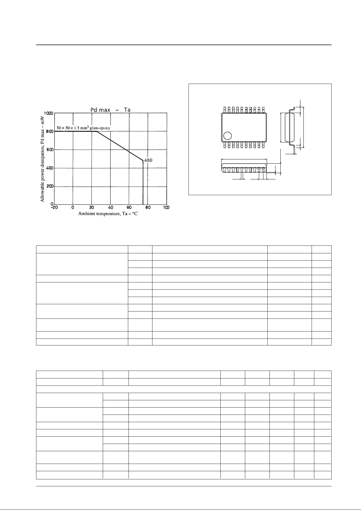
• Provided in the miniature ultrathin SSOP-20 package
(6.4 × 6.5 × 1.6 mm)
Package Dimensions
unit: mm
3179A-SSOP20
110
11
6.4
6.7
0.5
4.4
0.1
1.6max
1.0
20
0.650.22 0.43
0.15
SANYO: SSOP20
[LB8632V]
Parameter Symbol Conditions Ratings Unit
V
B
max 8.0 V
Maximum supply voltage V
S
max 8.0 V
V
DD
max 8.0 V
Output current I
O
max Between OUT1 and OUT2 (t ≤ 100 ms, single pulse) 3.0 A
V
OUT
1 OUT1, OUT2 VS+ V
F
V
Output supply voltage V
OUT
2 OUT3N, OUT3P V
S
V
V
OUT
3V
REF
V
B
V
Input supply voltage
V
IN
1 MD0 to MD2, IN1, IN2 V
DD
V
V
C
V
CONT
V
B
V
Allowable power dissipation Pd max
Mounted on a 50 × 50 × 1.5 mm3glass-epoxy printed
800 mW
circuit board
Operating temperature Topr –20 to +75 °C
Storage temperature Tstg –55 to +150 °C
Parameter Symbol Conditions min typ max Unit Note
Standby current I
B STB
VB= 7.5 V 0.1 1 µA 1
[DC motor system]
Operating voltage range 1
V
B
1VBsystem 1.2 7.5 V 2
V
S
1VBsystem 1.0 V
B
V3
Output saturation voltage
Vsat I
O
= 600 mA, VB= VS= VDD= 1.8 V 0.30 0.45 V 4
(pnp + npn)
Vsat I
O
= 1000 mA 0.45 0.65 V 4
Lower side output saturation voltage VsatN I
O
= 600 mA 0.15 0.25 V 24
Spark killer diode forward voltage V
F
IF= 600 mA 0.9 1.4 V 25
Output constant current
I
B
+
OUT3P –15 –20 –28 mA 5
I
B
–
OUT3N 15 20 28 mA 5
Operating current drain 1 I
B
1
V
B
+ VS(maximum forward/reverse/
80 98 mA 6
braking drive)
Operating current drain 2 IB2VB+ VS(standby in drive mode) 5.0 8.0 mA 7
Operating current drain 3 I
B
3VB+ VS(maximum single side drive) 50 70 mA 8
Page 3
Electrical Characteristics at Ta = 25°C, VB= VS= VDD= 3.0 V
Note: There are no limitations on the magnitude relationships between the VB, VSand VDDsupply voltages.
1. Stipulates the total leakage current for V
B
= VS= VDDwhen the IC is in standby mode.
2. Stipulates the operating range voltages (for guaranteed functionality) when a single power supply with V
B
= VS= VDDis used for the DC motor system.
3. Stipulates the operating range voltages (for guaranteed functionality) for the DC motor system V
S
pin, i.e., the motor power supply. The drive
current will be a constant current when V
B
= VS= 2.0 V or higher.
4. Stipulates the output saturation voltage when either the DC motor driver V
B
= VS= VDD= 1.8 V and the output current is 600 mA or when VB= V
S
= VDD= 3.0 V and the output current is 1000 mA.
5. Stipulates the current emitted or accepted by the OUT3P and OUT3N pins. These are constant currents as long as V
B
= VS= 2.0 V or higher.
6. Stipulates the maximum total current drain for the V
B
and VSpins for the forward, reverse, or brake operations when drive between the DC motor
system OUT1 and OUT2 outputs is used.
7. Stipulates the maximum total current drain for the V
B
and VSpins for the DC motor driver drive mode standby state.
8. Stipulates the maximum total current drain for the V
B
and VSpins for the DC motor driver single-sided drive mode, i.e. when a single output from
the OUT1, OUT2, OUT3P and OUT3N pins is used.
9. Stipulates the operating voltage range (for guaranteed functionality) for the V
REF
circuit system.
10.Stipulates the input voltage range for the Vcont pin. When a constant-voltage circuit is formed by adding an external transistor, the voltage is held
constant by sensing the V
CC
pin.
11.Stipulates the reference voltage generated at the V
REF
pin.
12.Stipulates the ratio of the constant V
CC
pin voltage value to the V
CONT
pin input voltage.
13.Stipulates the minimum output voltage for the V
CC
pin constant voltage output. The voltage will only fall to this value, even when the V
CONT
pin is
set to 0 V.
14.Stipulates the V
CC
pin stabilized output voltage when the V
REF
and V
CONT
pins are connected directly.
15.Stipulates the change in the value of the V
CC
voltage when VCCis set for constant voltage output and the VBvoltage varies from 2 V to 7.5 V.
16.Stipulates the change in the value of the V
CC
voltage when VCCis set for constant voltage output and the load current varies from 50 mA to 500
mA.
17.Stipulates the V
CONT
pin input current in the range 0 V ≤ V
CONT
≤ VB– 0.3 V. The value of the VCCoutput constant voltage can be varied by
inputting the CPU D/A output.
18.Stipulates the V
B
system maximum current drain in all modes when the VCCoutput has no load.
19.Stipulates the operating voltage range (for guaranteed functionality) for the V
DD
pin. The VDDpin is connected either to the CPU power supply or VB.
20.Stipulates the input current and allowable leakage current for the control input pins: MD0, MD1, MD2, IN1 and IN2.
21.Stipulates the high and low input voltages for the control input pins: MD0, MD1, MD2, IN1 and IN2. (When input pins are open, they appear to be
high-level inputs.)
22.Stipulates the V
DD
pin current drain when all the for the control input pins (MD0, MD1, MD2, IN1 and IN2) are at the ground level.
23.When the temperature exceeds the stipulated temperature, output current limitation is applied, thus protecting the IC. The stipulated temperature is
a design target value and is not tested prior to shipment.
24.Stipulates the lower side output saturation voltage in the OUT1 and OUT2 braking modes (when I
O
= 600 mA).
25.Stipulates the OUT1 and OUT2 spark killer diode forward voltage (when I
F
= 600 mA).
26.Stipulates the minimum value of the I
B
pin sink current.
No. 5161-3/18
LB8632V
Parameter Symbol Conditions min typ max Unit Note
[V
REF
system]
Operating voltage range 2 V
B
2 1.5 7.5 V 9
V
CONT
input voltage range V
CR
0V
B
V10
V
REF
voltage V
REFIREF
= 10 µA 1.29 1.36 1.43 V 11
I/O voltage ratio O
IR
VCC/V
CONT
1.35 1.37 1.39 Times 12
Minimum constant output voltage V
CC
min 0.8 0.9 V 13
Regulator voltage V
REG
V
REF
= V
CONT
, C2 = 10 µA 1.76 1.86 1.96 V 14
I
B
pin sink current I
IB
8.0 mA 26
Line regulation ∆V
OLN
2.0 V ≤ VB≤ 7.5 V 10 20 mV 15
Load regulation ∆V
OLD
50 mA ≤ ICC≤ 500 mA 20 50 mV 16
V
CONT
input current I
VC
1µA 17
Operating current drain 4 I
B
4VBsystem 5.0 8.0 mA 18
[V
DD
control input system]
V
DD
voltage range V
DR
1.2 7.5 V 19
Control pin input current
I
INL
V
INL
= GND, VDD= 3 V –120 –150 µA 20
I
INH
V
INH
= VDD, VDD= 3 V –3 0 µA 20
Input low-level voltage V
IL
–0.3 VDD– 1.0 V 21
Input high-level voltage V
IH
VDD– 0.3 V
DD
V21
Operating current drain I
VD
MD0, MD1, MD2, IN1 and IN2 = GND,
1.7 2.2 2.7 mA 22
V
DD
= 5 V
Thermal protection operating
T
SD
Design target value 180 °C 23
temperature
Page 4
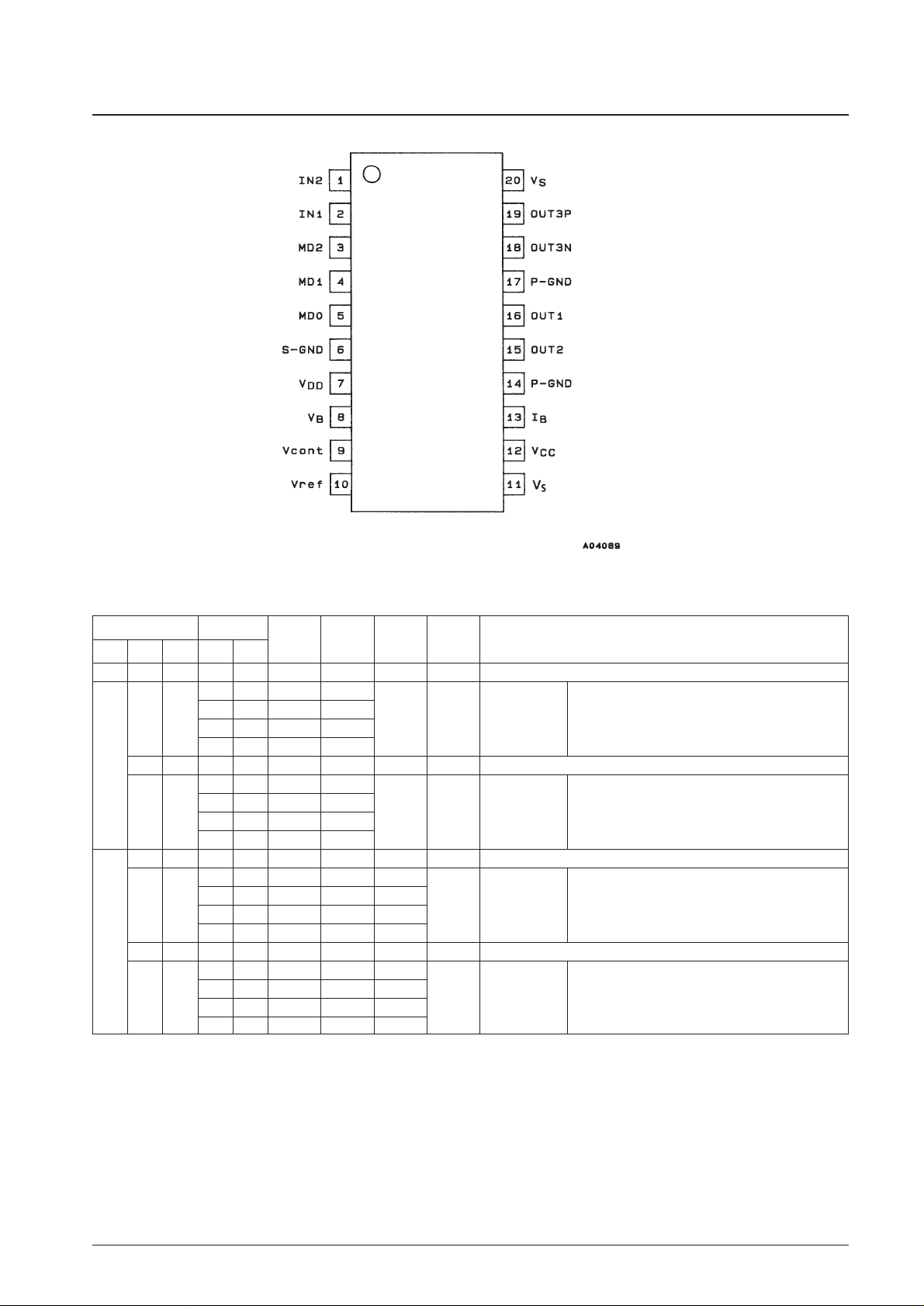
Pin Assignment
Truth Table (active low)
Note: The “—” entries for active-low/IN inputs are don’t care states, and the “—” entries for OUT outputs are OFF states.
See the sample application circuit for the motor number.
No. 5161-4/18
LB8632V
MD IN
OUT
OUT1 OUT2 3P V
CC
Note
01212
3N
H H H — — — — — — Standby (zero current drain)
HH — —
Standby
HL
HL L H
—On
Forward
Motor 1
LH H L
Reverse
LL L L
Brake
H L H — — — — — On The IN input is ignored. Motor 3 drive used.
HH — —
Standby
LL
HL — H
—On
Forward
Motor 2
LH — L
Reverse
LL — L
Brake
L L — — — — — On Only V
CC
on
HH — — —
Standby
HL
HL L — 3P
On
Forward Motor 4
LH H — 3N
Reverse External transistor
LL L — 3N
Brake
L
L H — — — — — On The IN input is ignored
HH — — —
Standby
HH
HL — — 3P
On
Forward Motor 5
LH — — 3N
Reverse External transistor
LL — — 3N
Brake
Note: Connect both P-GND pins and both VSpins.
Top view
Page 5
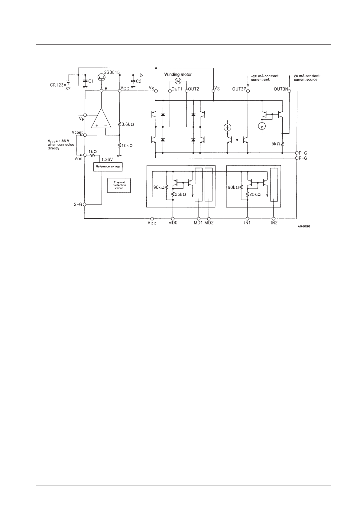
Internal Block Diagram
Wiring Notes
1. Connect both the P-GND and both the VSpins. Although both the P-GND and VSlines are connected internally,
both must be connected to provide currents of 1 A or over, or to provide even lower saturation output. However,
operation with only one of each of these pairs connected, or with through power supply wiring, is possible.
2. Since large currents flow in the VSand P-GND lines, these lines should be made thicker, and line impedance
reducing capacitors should be inserted in the vicinity of the IC.
3. Since S-GND is the ground for the control system, rather than using the same wiring as the P-GND line, it is
preferable to connect this pin to the CPU ground line.
4. If the CPU outputs are CMOS outputs, connect VDDto the CPU power supply line and if they are n-channel open
drain outputs, connect VDDto the VBpin (battery). However, since VDDis the control input system power supply, it
should not be set to the same impedance as the VSline.
No. 5161-5/18
LB8632V
Page 6
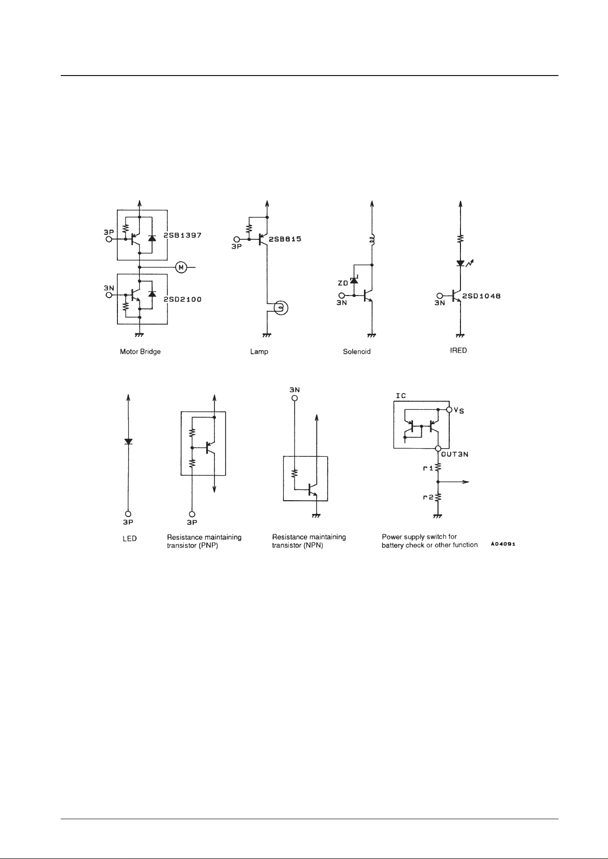
Sample OUT3P/OUT3N Pin Applications
The OUT3P and OUT3N pins support –20 mA (typical) and 20 mA (typical) constant current drive, respectively.
Constant current is supported when VB= VS= 2.0 V or higher. A 5 kΩ shunt resistor between the OUT3P pin and
ground is included within the IC. Inversely, the OUT3N pin is an open collector pin, and there is no resistor inserted
between this pin and the VSpin. A current limiting resistor (resistance maintaining transistor) may be inserted between
the OUT3P and OUT3N pins and the external transistors. These pins can also be used for direct LED drive, battery
check, or other power supply switching functions.
Recommended Transistors
Low-saturation transistors
2SB815/2SD1048 CP IO= 0.7 A
2SB1120/2SD1620 PCP IO= 2.5 A
Transistors with spark killer diodes and E-B resistors
CPH3120, 2SD2324 CP IO= 0.8 A
2SB1397/2SD2100 PCP IO= 2 A
Transistors with resistors
2SA1520/2SC3914 CP IO= 0.5 A
No. 5161-6/18
LB8632V
Page 7

Sample IBand VCCPin Applications
1. Stabilized Power Supply
A low-saturation type stabilized power supply can be formed using an external pnp transistor (2SB815). This circuit
has a wide operating voltage range of 1.5 to 7.5 V, and can supply stable power to other pins and loads. This circuit
outputs a constant voltage 1.37 times the Vcont input voltage. A 1.86 V constant voltage output can be acquired by
directly connecting the V
REF
reference voltage (1.36 V) to the Vcont pin.
• This circuit sets up a constant voltage output of 1.86 V or lower.
When R1 is 20 kΩ, the output voltage can be set to any voltage
between 0.8 and 1.86 V (typical) by adjusting R2.
• This circuit sets up a constant voltage output of 1.86 V or higher.
Taking the manufacturing variation in the IC internal sensing resistor
(3.6 to 10 kΩ) into account, the total resistance of the external
sensing resistors (R1 and R2) should be about 1 kΩ.
Example: A constant voltage output V
REG
of 3.05 V is acquired
when R1 is 360 Ω and R2 is 680 Ω.
• Making the OUT pin output voltage a constant voltage.
Connect the OUT pin, which is to be made a constant voltage output,
to the VCCpin. When one side of the bridge output is connected,
when the connected side is a high-level output the circuit will be a
constant voltage drive circuit, and when the other side is a high-level
output the circuit will be a saturated drive circuit.
• Generating a hold voltage.
This circuit uses a resistance maintaining transistor to lower the
V
CONT
input and generate a hold voltage.
A 0.8 V (typical) hold voltage is acquired when R2 is 0 Ω.
• Generating a set constant voltage for different modes.
The V
CONT
input has a high impedance of 1 µA maximum, and thus
the set constant voltage can be changed as required for each mode by
inputting the CPU D/A converter output.
No. 5161-7/18
LB8632V
Page 8

2. Battery Check
Tr2 will turn off when the Vcont input voltage, which is VB× , falls to 0.95 V or lower.
Example: This circuit can check for VBbeing 2.0 V or lower by setting r1 to be 22 kΩ and r2 to be 20 kΩ. Note that
the Tr3 transistor can also use the OUT3N output.
3. Light Measurement
Tr2 will turn on when the V
CONT
input voltage becomes VB× 70% (= 9 kΩ/(3.6 kΩ + 10 kΩ)) or higher. Note that
the Tr3 transistor can also use the OUT3N output.
r2
r2 + r1
No. 5161-8/18
LB8632V
Page 9

Power Supply Specifications
1. Single Supply Specifications
2. Step-Up Supply Specifications
No. 5161-9/18
LB8632V
Page 10

Sample Application 1
Sample Application 2
No. 5161-10/18
LB8632V
MD
Mode
02
H H Standby (zero current drain)
H L Motor 1
L H Solenoid, battery check
MD
Mode
2
H Standby (zero current drain)
L Motor 1 (single-direction regulator output)
Page 11

Sample Application 3
Sample Application 4
No. 5161-11/18
LB8632V
MD
Mode
02
H H Standby (zero current drain)
H L Motor 1 (single-direction regulator output)
LHV
S
line saturated output (battery voltage switch)
L L Motor 4 (single-direction regulator output)
MD
Mode
02
H H Standby (zero current drain)
H L Motor 1
L H Only the V
CC
regulator output on
L L Motor 4 (single-direction regulator output)
Page 12

Sample Application 5
Sample Application 6
No. 5161-12/18
LB8632V
MD
Mode
012
H H H Standby (zero current drain)
H H L Motor 1
H L H Motor 3 (bidirectional regulator output)
H L L Motor 2 (single-direction regulator output)
L L L Only the V
CC
regulator output on
L L H Motor 4 (bidirectional regulator output)
L H H IRED, LED
MD
Mode
12
H H Standby (zero current drain)
H L Motor 1
L H Motor 3 (bidirectional regulator output)
L L Motor 2 (single-direction regulator output)
Page 13

Sample Application 7
No. 5161-13/18
LB8632V
MD
Mode
012
H H H Standby (zero current drain)
H H L Motor 1 (bidirectional regulator output)
H L H Motor 3 (bidirectional regulator output)
H L L Motor 2 (bidirectional regulator output)
L L L Only the V
CC
regulator output on
L H H Motor 5 (H bridge formed using external transistors)
Page 14

Truth Table for Two LB8632V ICs
This truth table specifies the logic when using two LB8632V ICs (IC1 and IC2). As shown in the figure below, the five
lines from the CPU should be connected to MD0, MD1, MD2, IN1, and IN2 for IC1 and to MD0, MD2, MD1, IN2, and
IN1 for IC2, respectively.
Note: The “—” entries for active-low/IN inputs are don’t care states, and the “—” entries for OUT outputs are OFF states.
See the sample application circuit for the motor number.
No. 5161-14/18
LB8632V
MD IN
IC1 IC2
OUT1 OUT2
OUT3 OUT3
OUT2 OUT1
OUT3 OUT3
V
CC
Note
01212
PNP NPN PNP NPN
HHH———————————Standby (zero current drain)
HH————————
Standby
HL
HLL H——————
On
Forward
Motor 1
LHH L ——————
Reverse
LLL L —— ————
Brake
HH————————
Standby
HLH
HL———— L H——
On
Forward
Motor 3
LH———— H L ——
Reverse
LL———— L L ——
Brake
HH————————
Standby
LL
HL—H——L———
On
Forward
Motor 2
LH— L —— H———
Reverse
LL— L —— L ———
Brake
LL——————————OnOnly V
CC
on
HH————————
HL
HLL —On— ————
On
LHH——On————
LLL——On————
HH————————
Standby
L
LH
HL————— H —On
On
Forward Motor 4
LH———— — LOn—
Reverse External transistor
LL———— — L —On
Brake
HH————————
Standby
HH
HL——On————On
On
Forward Motor 5
LH———On——On—
Reverse External transistor
LL———On———On
Brake
Page 15

No. 5161-15/18
LB8632V
Page 16

No. 5161-16/18
LB8632V
Page 17

No. 5161-17/18
LB8632V
Page 18

PS No. 5161-18/18
LB8632V
This catalog provides information as of February, 2000. Specifications and information herein are subject
to change without notice.
Specifications of any and all SANYO products described or contained herein stipulate the performance,
characteristics, and functions of the described products in the independent state, and are not guarantees
of the performance, characteristics, and functions of the described products as mounted in the customer’s
products or equipment. To verify symptoms and states that cannot be evaluated in an independent device,
the customer should always evaluate and test devices mounted in the customer’s products or equipment.
SANYO Electric Co., Ltd. strives to supply high-quality high-reliability products. However, any and all
semiconductor products fail with some probability. It is possible that these probabilistic failures could
give rise to accidents or events that could endanger human lives, that could give rise to smoke or fire,
or that could cause damage to other property. When designing equipment, adopt safety measures so
that these kinds of accidents or events cannot occur. Such measures include but are not limited to protective
circuits and error prevention circuits for safe design, redundant design, and structural design.
In the event that any or all SANYO products (including technical data, services) described or contained
herein are controlled under any of applicable local export control laws and regulations, such products must
not be exported without obtaining the export license from the authorities concerned in accordance with the
above law.
No part of this publication may be reproduced or transmitted in any form or by any means, electronic or
mechanical, including photocopying and recording, or any information storage or retrieval system,
or otherwise, without the prior written permission of SANYO Electric Co., Ltd.
Any and all information described or contained herein are subject to change without notice due to
product/technology improvement, etc. When designing equipment, refer to the “Delivery Specification”
for the SANYO product that you intend to use.
Information (including circuit diagrams and circuit parameters) herein is for example only; it is not
guaranteed for volume production. SANYO believes information herein is accurate and reliable, but
no guarantees are made or implied regarding its use or any infringements of intellectual property rights
or other rights of third parties.
 Loading...