

SANYO LB8109M Datasheet

Ordering number: EN5233
Monolithic Digital IC
LB8109M
Actuator Driver for Portable CD Players
Overview
The LB8109M is an actuator driver IC designed for portable
CD players that operate at 2.4 V (two Ni-Cd batteries) or 3.0 V
(two dry cells).
Package Dimensions
unit : mm
3148-QIP44MA
[LB8109M]
SANYO : QIP44MA
Functions and Features
.
H bridge drivers (output dynamic range maximum is about 2 V) on chip for four channels to drive each CD actuator (the focus
coil, the tracking coil, the spindle motor, and the sled motor).
.
Step-up circuit (voltage to be set by an external resistor) on chip that is used to apply voltage to the CD DSP, ASP and
microcontroller. Center-tap coil for step-up circuit makes it possible to supply the driver control voltage. (However, the drive Tr,
L, C, and Di are all external.)
.
Oscillator circuits for each converter on chip. (C and R are external.)
.
Four-channel driver control output is divided into two groups (the focus/tracking group and the spindle/sled group) for minimum
loss at double-speed play.
Higher operating voltage in each group is converted to power supply of each 2ch H bridge driver by PMW conversion.
(However, the PWM PNP-Tr, NPN-Tr, L, C, and Di are all external.)
.
Sled motor driving mode is switchable between step drive mode for lower power dissipation, and normal V-type drive mode.
(The other three channels are fixed to V-type.)
.
In the spindle motor drive circuit, the control gain can be doubled for double-speed play. (Switching port provided.)
.
PWM step-down circuit for external power operates when external power (8 V or more) is supplied.
In this function, external power is converted to V
In play mode, step-up voltage for DSP has to be set lower than V
V
.
CC
So step-down voltage (V
(However, the PWM PNP-Tr, NPN-Tr, L, C, and Di are all external.)
.
Battery pulse charging function on chip. (However, the drive NPN-Tr, and the current feedback C and R are external.)
.
Having one 358-type OP amplifier on chip, it is suitable for a variety of applications. (Power supply: VCD)
.
The system can be started up and stopped by outputs from the microcontroller.
.
Actuator muting function on chip (for all four channels simultaneously).
.
Thermal shutdown circuit on chip.
) setting of two types is possible with two pairs of external resistor. (Switching port is provided.)
CC
power supply, and two type voltage setting is possible.
CC
, but in charging the battery, it has to be set higher than
CC
SANYO Electric Co.,Ltd. Semiconductor Bussiness Headquarters
TOKYO OFFICE Tokyo Bldg., 1-10, 1 Chome, Ueno, Taito-ku, TOKYO, 110 JAPAN
13096HA (II) No.5233-1/9

LB8109M
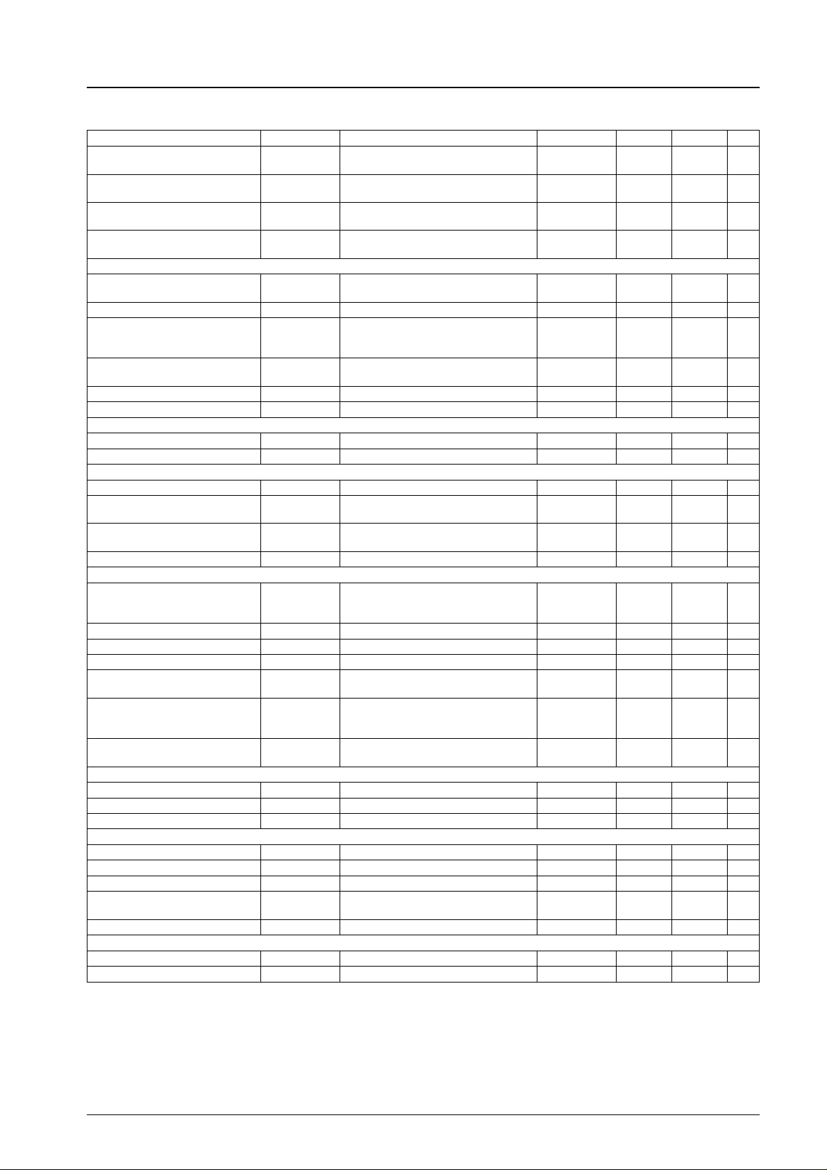
Specifications
Absolute Maximum Ratings atTa=25°C
Parameter Symbol Conditions Ratings Unit
Maximum supply voltage V
V
pin input voltage VCDmax 10 V
CD
H bridge output current I
Allowable power dissipation Pd max Independant IC 700 mW
Operating temperature Topr –20 to +75
Storage temperature Tstg –55 to +150
Allowable Operating Ranges at Ta = 25°C
Parameter Symbol Conditions Ratings Unit
Supply voltage V
V
pin input voltage V
CD
V
drop setting voltage when
CC
external voltage input is applied
Electrical Characteristics atTa=25°C, VCC=3V,VCD=4V
max 7V
CC
max Maximum per channel is 400 mA. 800 mA
OUT
CC
CD
V
CC(EXT)
1.6 to 5.0 V
3.6 to 9.0 V
3.0 to 5.0 V
C
°
C
°
Parameter Symbol Conditions min typ max Unit
[Power Supply Block]
Standby current drain I
V
no-signal current drain I
CC
V
no-signal current drain I
CD
CCO
CC
CD
S/S = [H], the total of VCCand V
CD
S/S = [L], VCCline only 7.0 10.0 mA
S/S = [L], with no driver input 5.0 8.0 mA
[Externally set step-up circuit]
ASP drive output current I
Reference voltage of step-up
circuit
pin input bias current I
V
ASP
UPBASE pin saturation
voltage
V
Load regulation R
Line regulation R
Minimum off duty D
O ASPDRVVASP
V
ref ASP
B V ASP
O UPBASEIO
LD ASP
LN ASP
min ASP
= 1 V 2.2 2.8 3.4 mA
Determined at ASP drive pin 1.23 1.28 1.33 V
V
= 1.5 V 200 nA
ASP
= 1 mA 0.2 V
V
= 3.5 V, L = 30 µH, C = 220 µF 1000 mV/A
ASP
V
= 3.5 V, L = 30 µH, C = 220 µF 100 mV/V
ASP
[S/S Pin Function]
S/S start voltage V
S/S off voltage V
ON VCC–1.0 V
SS
OFF VCC–0.5 V
SS
[H Bridge Output Block, PWM Block]
Output saturation voltage V
V
pin maximum output
OUT
voltage
V
PWM applied offset voltage V
H sat
OUT
PWMOFF
IO= 200 mA, TOP + BOTTOM 0.30 0.45 V
max 2.25 V
At mute state (each output = 0) 0.23 0.26 0.29 V
DNB – 1,2 pins output current Io DNB1,2 V
Load regulation R
Line regulation R
LDVOUTVOUT
LNVOUTVOUT
= max, L = 30 µH 1000 mV/A
= max, L = 30 µH 100 mV/V
[Drive Control Block]
CH1 to 4 input voltage range V
ASP REF input voltage range V
Input bias current I
Input offset voltage V
IN1–4
ASPR
BIN
off IN
CH1,2,4 transfer gain G124
CH3 L side transfer gain G3L
CH3 H side transfer gain G3H
Each VIN=V
V
ASP REF
RL=10Ω 7.1 8.3 9.5 dB
IN
RL=10Ω 7.1 8.3 9.5 dB
IN
RL=10Ω 13.6 14.8 16.0 dB
IN
ASP REF
= 2 V –30 +30 mV
= 2 V 2.0 µA
0.5 VCD–0.5 V
1.2 VCD–1.3 V
20 µA
20 %
/600 A
OUT
Continued on next page.
No.5233-2/9
LB8109M
Continued from preceding page.
Parameter Symbol Conditions min typ max Unit
Negative/positive transfer gain
difference
Input dead zone voltage range V
G-SELECT pin low-gain side
selection voltage
G-SELECT pin high-gain side
selection voltage
[SLED Drive Circuit]
SL REF pin input voltage
range
SL REF pin input bias current I
Positive side setting offset
voltage between IN4
and SL REF
Dual side step width difference
voltage
SL MODE pin high voltage V
SL MODE pin low voltage V
[Muting Block]
Mute on voltage V
Mute off voltage V
[OP Amplifier Block]
Input offset voltage V
Input bias current for each
input
Common-mode input voltage
range
Open-loop voltage gain G
[External Voltage Input Block]
Minimum operating input
voltage when external voltage
input is applied
EXTDRV pin output current I
VZ pin voltage V
VZ pin inflow current I
V
EXT,VEXT
Input bias current
V
EXT,VEXT
Step-up circuit reference
-CHG pin
-CHG pin
voltage
EXTBASE pin saturation
voltage
[OSC Block]
OSCPWR pin output voltage V
Maximum oscillation frequency F
Input bias current I
[Pulse Charging Function]
Internal reference voltage V
CHG-ON pin ON voltage V
CHG-ON Pin OFF voltage V
CHG-MON pin input bias
current
CHGDRV pin output current I
[TSD Block]
Operating temperature T
Temperature hysteresis width ∆T
Note 1: For parameters which have an entry of ‘‘design target value’’ in the ‘‘Conditions’’ column, no measurements are made.
∆G
DZ
V
GSELL-TH
V
GSELH-TH
V
SL REF
B SL REFVSL REF
V
off SL REFVSL REF
V
SL DIFF
H SL MODE
L SL MODE
ON MUTE
OFF MUTE
OFF OP
I
BOP
V
CM OP
VOP
V
I EXT
O EXT DRVVEXT
Z
VZ
I
B EXTCHG
I
B EXT
Vref
E-CHG
Vref
EXT
V
EXTBASEIO
OSCPWR
OSC max
B OSC
CHG REF
CHG-ON
CHG-OFF
I
B CHG MONVCHG MON
O CHG DRVVCHG MON
TSD
TSD
RL=10Ω –1.0 0 +1.0 dB
IN
RL=10Ω, output voltage difference
5 mV or less
V
SL REF
OPin(+) = OPin(–)=2V 200 nA
atf=10kHz 31 34 37 dB
RIN=1kΩ 8.0 V
= 1 V (CHG-ON [L]) 170 210 250 µA
V
=10V,RIN=1kΩ 6.4 6.9 7.4 V
EXT
V
= 1.5 V
EXT
V
EXT-CHG
Both determined at EXTDRV pin
EXT-CHG side: CHG-ON [H]
= 1 mA 0.2 V
V
= 0 V –2.0 µA
OSC
Design target value, Note 1 180
Design target value, Note 1 20
030mV
2.0 V
1.0 V
V
+0.1 VCD–1.0 V
ASP REF
= 2 V 200 nA
= 2.3 V, V
= 2.3 V, V
ASP REF
ASP REF
= 2 V –20 +20 mV
= 2 V –25 +25 mV
2.0 V
1.0 V
2.0 V
1.0 V
–5 +5 mV
VCD–1.5 V
20 mA
= 1.5 V (CHG-ON [H])
200 nA
1.23 1.28 1.33 V
VCC–0.15 V
100 kHz
0.32 0.35 0.38 V
2.0 V
1.0 V
= 0.3 V 200 nA
= 0 V 2.4 3.0 3.6 mA
C
°
C
°
No.5233-3/9
 Loading...