

SANYO LA4592W Datasheet
Overview
The LA4592W is a single-chip 1.5-V headphone stereo
system IC. The LA4592W adds a variety of functions,
including a switch amplifier (for end product audio quality
switches, the metal tape switch, and other switches) and an
AMSS (Automatic Music Search System) function that
supports blank skipping, to the earlier LA4590W.
Furthermore, the LA4592W provides even lower no-signal
time power levels for lower end-product power
dissipation. In combination with the LA3235W 1.5-V
record preamplifier IC, the LA4592W can be used to
implement a record/playback cassette system with just two
ICs.
Functions
• Stereo preamplifier: supports auto reverse and includes a
muting function.
• Stereo power amplifier: Includes OCL and muting
functions.
• Ripple filter
• Low boost function (BTL operation in the lowfrequency region)
• Inter-track detection function (Supports AMSS and
blank skipping)
• Two switching amplifiers
• Power switch (standby function)
Features
• Virtual ground impedance is reduced by built-in V
REF
amplifier
• No capacitor required for ripple filter oscillation
prevention.
• Provides ample output power at low frequencies.
(PO= 24 mW, VCC= 1.2 V, f = 150 Hz)
• High-frequency cutoff capacitors built into the
preamplifier and power amplifier inputs to minimize
buzzing.
Monolithic Linear IC
Ordering number : EN5662
73097HA (OT) No. 5662-1/5
SANYO: SQFP48
[LA4592W]
SANYO Electric Co.,Ltd. Semiconductor Bussiness Headquarters
TOKYO OFFICE Tokyo Bldg., 1-10, 1 Chome, Ueno, Taito-ku, TOKYO, 110 JAPAN
1.5-V Preamplifier + Power Amplifier
for Headphone Stereo Products
LA4592W
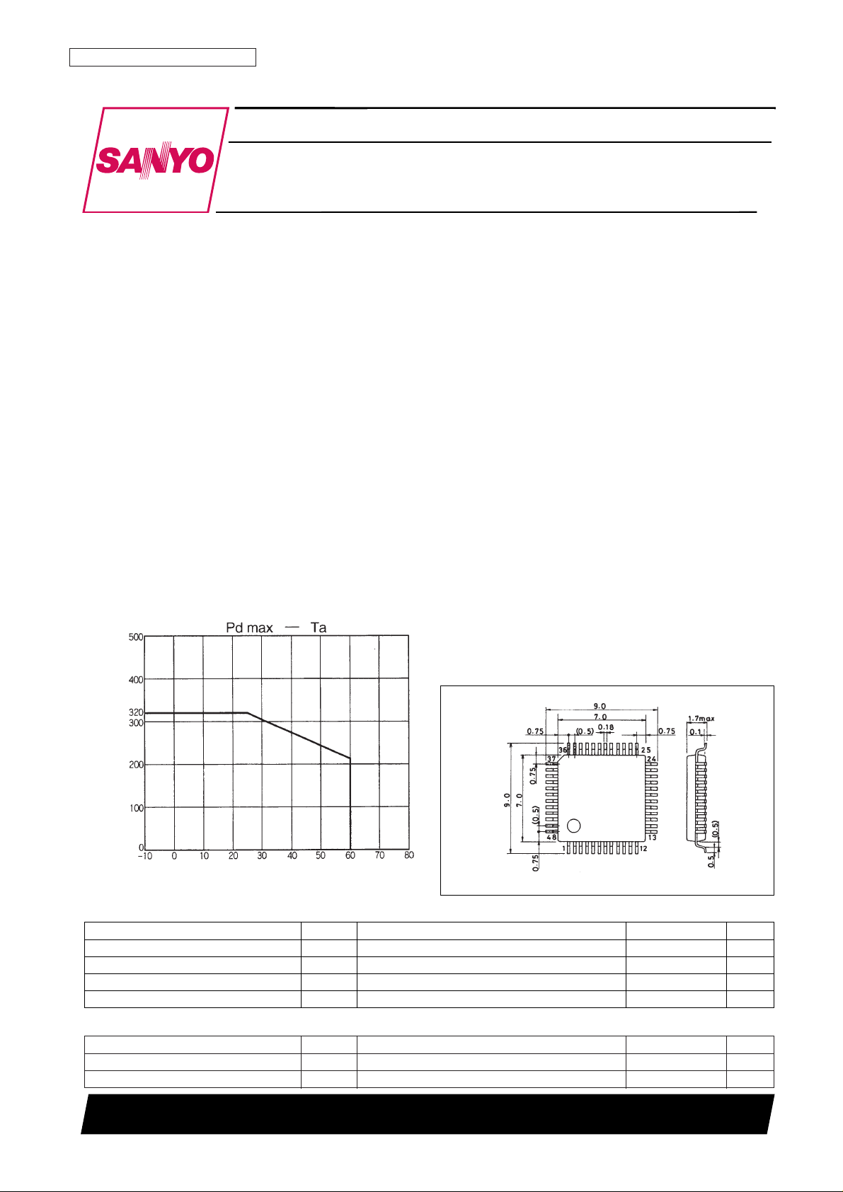
Package Dimensions
unit: mm
3163A-SQFP48
Parameter Symbol Conditions Ratings Unit
Maximum supply voltage V
CC
max 3.0 V
Allowable power dissipation Pd max 320 mW
Operating temperature Topr –10 to +60 °C
Storage temperature Tstg –40 to +125 °C
Specifications
Maximum Ratings at Ta = 25°C
Parameter Symbol Conditions Ratings Unit
Recommended supply voltage V
CC
1.5 V
Operating supply voltage range V
CC
op 0.95 to 2.2 V
Allowable Operating Ranges at Ta = 25°C
Ambient temperature, Ta – °C
Allowable power dissipation, Pd max – W
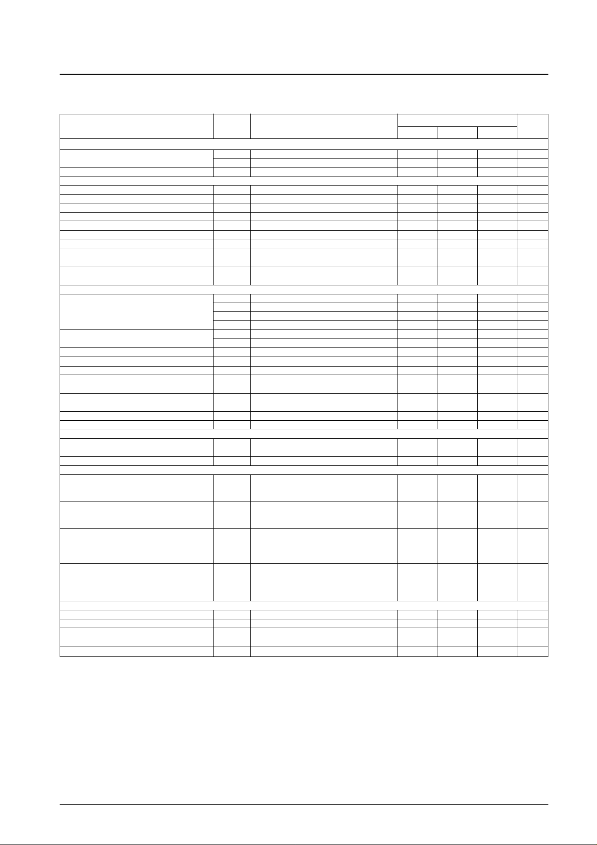
No. 5662-2/5
LA4592W
Parameter Symbol Conditions
Ratings
Unit
min typ max
[PRE + PWR]
Quiescent current
I
CCO
1 Rg = 2.2 kΩ, RV= 0 Ω 8.5 11 16 mA
I
CCO
2 With the power switch off 0.1 5 µA
Voltage gain (closed loop) VG
TVO
= –20 dBm, RV= 10 kΩ 54 57 60 dB
[PRE AMP]
Voltage gain (open loop) VG
0VO
= –20dBm 60 68 dB
Voltage gain (closed loop) VG
1VO
= –20dBm 34 35.3 37 dB
Maximum output voltage V
O
max1 THD = 1 % 100 210 mV
Total harmonic distortion THD1 VG = 35.3 dB/NAB, V
O
= 100 mV 0.08 0.5 %
Equivalent input noise voltage V
N
1 Rg = 2.2 kΩ, BPF = 20 Hz to 20 kHz 1.3 3.0 µV
Interchannel crosstalk CT1 Rg = 2.2 kΩ, TUNE 1 kHz, V
O
= –20 dBm 45 56 dB
F/R crosstalk CT2 Rg = 2.2 kΩ, TUNE 1 kHz, V
O
= –20 dBm 65 78 dB
Ripple rejection ratio Rr1
Rg = 2.2 kΩ, Vr = –30 dBm,
45 52 dB
fr = 100 Hz, TUNE 100 Hz
Muting output voltage V
M
1
V
IN
= –40 dBm, TUNR 1 kHz,
–90 dBm
With the muting function on
[Low Boost + Power Amplifier]
VG
3VO
= –20 dBm 20.5 23 25.5 dB
Voltage gain (closed loop)
VG
4VO
= –20 dBm, L.B = ON 20.5 23 25.5 dB
VG
5VO
= –20 dBm, L.B = ON, f = 10 kHz 24.5 27.5 30.5 dB
VG
6VO
= –20 dBm, L.B = ON, f = 100 Hz 28 32 36 dB
Output voltage
P
O
1 THD = 10 % 5 9 mW
P
O
2 THD = 10 %, f = 100 Hz, L.B = ON 13 19 mW
Total harmonic distortion THD2 P
O
= 1 mW 0.3 1.5 %
Interchannel crosstalk CT3 V
O
= –20 dBm, RV= 0 Ω 38 43 dB
Output noise voltage V
NORV
= 0 Ω, BPF = 20 Hz to 20 kHz 20 33 µV
Ripple rejection ratio Rr2
R
V
= 0 Ω, Vr = –30 dBm,
50 74 dB
fr = 100 Hz, TUNE 100 Hz
Muting output voltage V
M
2
V
IN
= –30 dBm, TUNE 1 kHz,
–90 dBm
With the muting function on
Input resistance Ri 8 10 12 kΩ
Voltage gain difference ∆VG3 0 1.5 dB
[Ripple Filter]
Ripple rejection ratio R
r
3
fr = 100 Hz, Vr = –30 dBm, V
CC
= 1.0 V,
33 39 dB
IRF= 25 mA, using a rank 6 2SB1295
Output voltage V
RF
VCC= 1.0 V, IRF= 25 mA 0.89 0.94 V
[AMSS]
The preamplifier output voltage
Operating output voltage V
OAMSS
1 when the AMSS VO= 0.6 V p-o 3.33 4.7 6.64 mV
With the PWR muting on. (AMSS)
The preamplifier output voltage
Operating output voltage V
OAMSS
2 when the AMSS VO= 0.6 V p-o 479 675 953 µV
With the PWR muting off. (BLANK SKIP)
The preamplifier output voltage
Operating output voltage V
OAMSS
3
when the AMSS V
O
= 0.6 V p-o
2.62 3.7 5.23 mV
With pin 34 shorted through a 270-Ω resistor.
With the PWR muting on.
The preamplifier output voltage
Operating output voltage V
OAMSS
4
when the AMSS V
O
= 0.6 V p-o
375 530 749 µV
With pin 34 shorted through a 270-Ω resistor.
With the PWR muting on.
[SW AMP]
Voltage gain (closed loop) VG7VO= –25 dBm –1.2 –0.7 –0.2 dB
Maximum output voltage V
O
max2 THD = 1 % 25 60 mV
Ripple rejection ratio Rr4
With the input pins open, Vr = –30 dBm,
50 75 dB
fr = 100 Hz, TUNE 100 Hz
Output voltage when off V
M
3 VIN= –20 dBm, TUNE 1 kHz, SW OFF –90 dBm
Operating Characteristics at Ta = 25°C, VCC= 1.2 V, f = 1 kHz, 0.775 V = 0 dB, RL= 10 kΩ (preamplifier)
RL = 16 Ω (power amplifier)
 Loading...