

SANYO LA4587M Datasheet
Ordering number: EN5204A
Monolithic Linear IC
LA4587M
Preamplifier + Power Amplifier
for 1.5 V Headphone Stereos
Overview
The LA4587M is a system IC that includes all of the necessary
functions for a playback set on a single chip, reducing the
number of external components needed.
Functions
.
Stereo preamplifier (supports auto reverse function,
switchable between metal and normal tape)
.
Stereo power amplifier (OCL, mute function)
.
Ripple filter
.
Low boost function (BTL operation in low-frequency range)
.
AMSS (Automatic Music Select System)
.
Power switch
Features
.
Preamplifier has a high open-loop gain (VGO= 73 dB).
.
Preamplifier requires no NF capacitor.
.
Virtual ground capacitor can be 1 µF or less. (Lower
impedance is achieved by having a V
.
Ripple filter requires no capacitor for preventing oscillation.
.
Powerful output is obtained in low boost output
(Po = 21 mW/V
.
A high-frequency cutoff capacitor is built into the
preamplifier and power amplifier inputs; anti-buzz provision.
= 1.2 V, f = 100 Hz).
CC
amplifier built in.)
REF
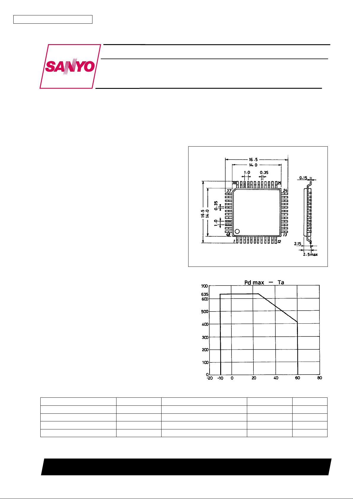
Package Dimensions
unit : mm
3102-QFP48D
[LA4587M]
SANYO : QIP48D
Specifications
Maximum Ratings atTa=25°C
Parameter Symbol Conditions Ratings Unit
Maximum supply voltage V
Allowable power dissipation Pd max 635 mW
Operating temperature Topr –10 to +60
Storage temperature Tstg –40 to +125
max 3.0 V
CC
Allowable power dissipation, Pd max − mW
Ambient temperature, Ta −°C
SANYO Electric Co.,Ltd. Semiconductor Bussiness Headquarters
TOKYO OFFICE Tokyo Bldg., 1-10, 1 Chome, Ueno, Taito-ku, TOKYO, 110 JAPAN
13097HA(II)/N3095HA(II) No.5204-1/18
C
°
C
°
LA4587M
Operating Conditions atTa=25°C
Parameter Symbol Conditions Ratings Unit
Recommended supply voltage V
Operating supply voltage range V
CC
op 0.95 to 2.2 V
CC
Operation Characteristics atTa=25°C, VCC=1.2V,f=1kHz, 0.775 V = 0 dBm,
=10kΩ(preamplifier), RL=16Ω(power amplifier)
R
L
Parameter Symbol Conditions min typ max Unit
[Preamplifier + Power Amplifier]
I
1 Rg = 2.2 kΩ,Rv=0Ω 81524mA
Quiescent current
Voltage gain (closed) VG
[Preamplifier]
Voltage gain (open) VG
Voltage gain (closed)
Maximum output voltage V
Total harmonic distortion THD
Equivalent input noise voltage V
Interchannel crosstalk CT
Interchannel crosstalk between
F and R
Ripple rejection ratio Rr1
[Low Boost + Power Amplifier]
Voltage gain (closed)
Output power
Total harmonic distortion THD
Interchannel crosstalk CT
Output noise voltage V
Ripple rejection ratio Rr
Output mute voltage V
Input resistance Ri 8 10 12 kΩ
Voltage gain difference ∆VG
[Ripple Filter ]
Ripple rejection ratio Rr
Output voltage V
[AMSS]
Operating output voltage V
CCO
I
2 When power switch is off 0.1 5 µA
CCO
VG
VG
max THD=1% 100 210 mV
O
NI
CT
VO= –20 dBm, RV=10kΩ 54 57 60 dB
T
VO= –20 dBm 60 73 dB
0
VO= –20 dBm 34 35.5 37 dB
1
VO= –20 dBm, f = 10 kHz, metal on 25.5 28 30.5 dB
2
VG = 35.5 dB/NAB, VO= 100 mV 0.1 0.5 %
1
Rg = 2.2 kΩ, BPF: 20 Hz to 20 kHz 1.3 3.0 µV
Rg = 2.2 kΩ, 1 kHz TUNE, VO= –20 dBm 45 56 dB
1
Rg = 2.2 kΩ, 1 kHz TUNE, VO= –20 dBm 65 78 dB
2
Rg = 2.2 kΩ, Vr = –30 dBm,
fr = 100 Hz, 100 Hz TUNE
VG
VG
VG
VG
P
O1
P
O2
NO
M
RF
OAMSS
VO= –20 dBm 20.5 23 25.5 dB
3
VO= –20 dBm, L.B. = on 20.5 23 25.5 dB
4
VO= –20 dBm, L.B. = on,f=10kHz 24.5 27.5 30.5 dB
5
VO= –20 dBm, L.B. = on, f = 100 Hz 30 34 38 dB
6
THD=10% 5 9 mW
THD = 10 %, f = 100 Hz, L.B. = on 13 21 mW
PO= 1 mW 0.5 1.5 %
2
VO= –20 dBm, RV=0Ω 38 43 dB
3
RV=0Ω, BPF: 20 Hz to 20 kHz 35 48 µV
RV=0Ω, Vr = –30 dBm,
2
fr = 100 Hz, 100 Hz TUNE
VIN= –30 dBm, 1 KHz TUNE, mute on –85 dBm
3
fr = 100 Hz, Vr = –30 dBm, VCC= 1.0 V,
3
I
= 25 mA, 2SB1295, hFE6 rank used
RF
VCC= 1.0 V, IRF= 25 mA 0.89 0.93 V
Preout voltage when AMSS VO= 0.6 Vp-p
Pin 34 is short-circuited through 270 kΩ.
1.5 V
45 52 dB
50 74 dB
0 +1.5 dB
33 39 dB
1.80 2.55 3.60 mV
Note: L.B. = Low boost
No.5204-2/18
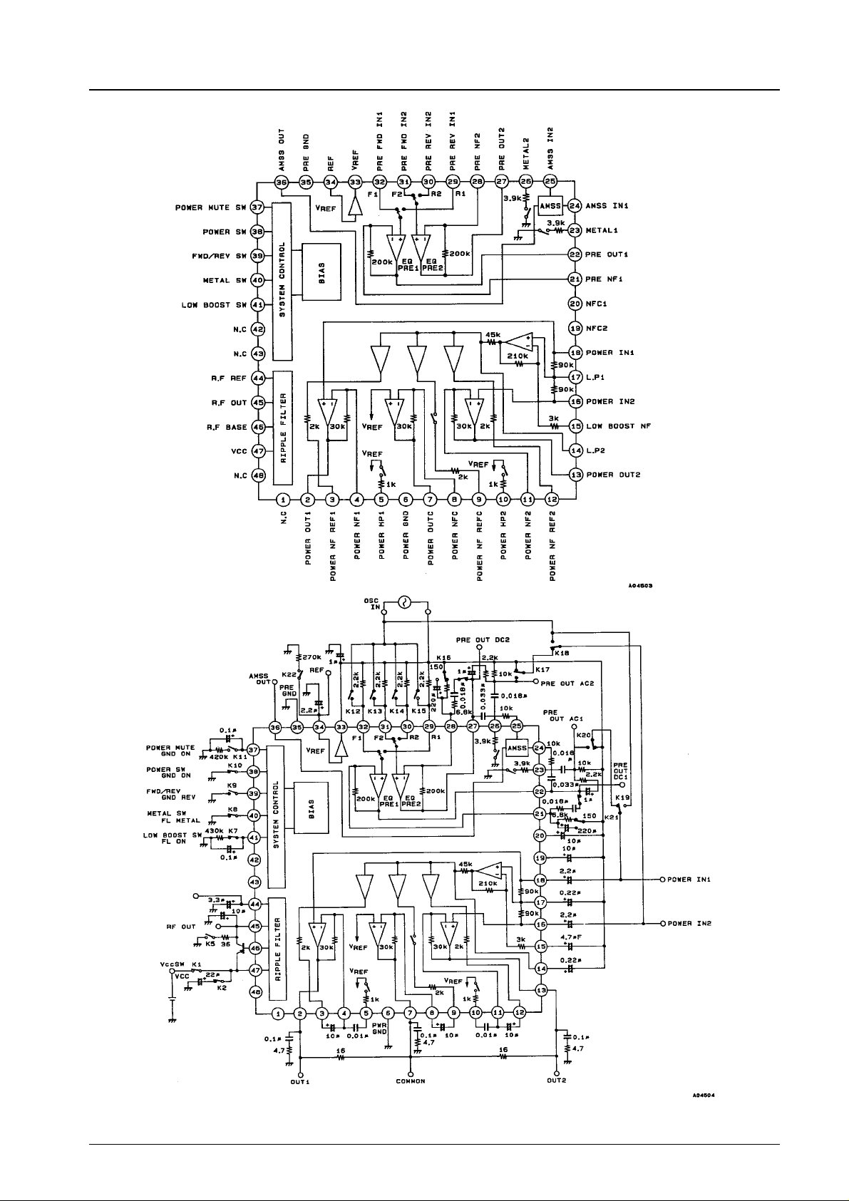
Block Diagram
LA4587M
Test Circuit Diagram
Unit (resistance: Ω)
Unit (resistance: Ω, capacitance: F)
No.5204-3/18

Sample Application Circuit
LA4587M
Unit (resistance: Ω, capacitance: F)
Note 1: Transistors equivalent to the 2SB1295 with hFE6 rank and upward are recommended.
Note 2: C18, C23, and C26 are oscillation prevention capacitors; a polyester film or ceramic capacitor (which can guarantee the
specified capacitance at operating temperatures) is recommended.
No.5204-4/18
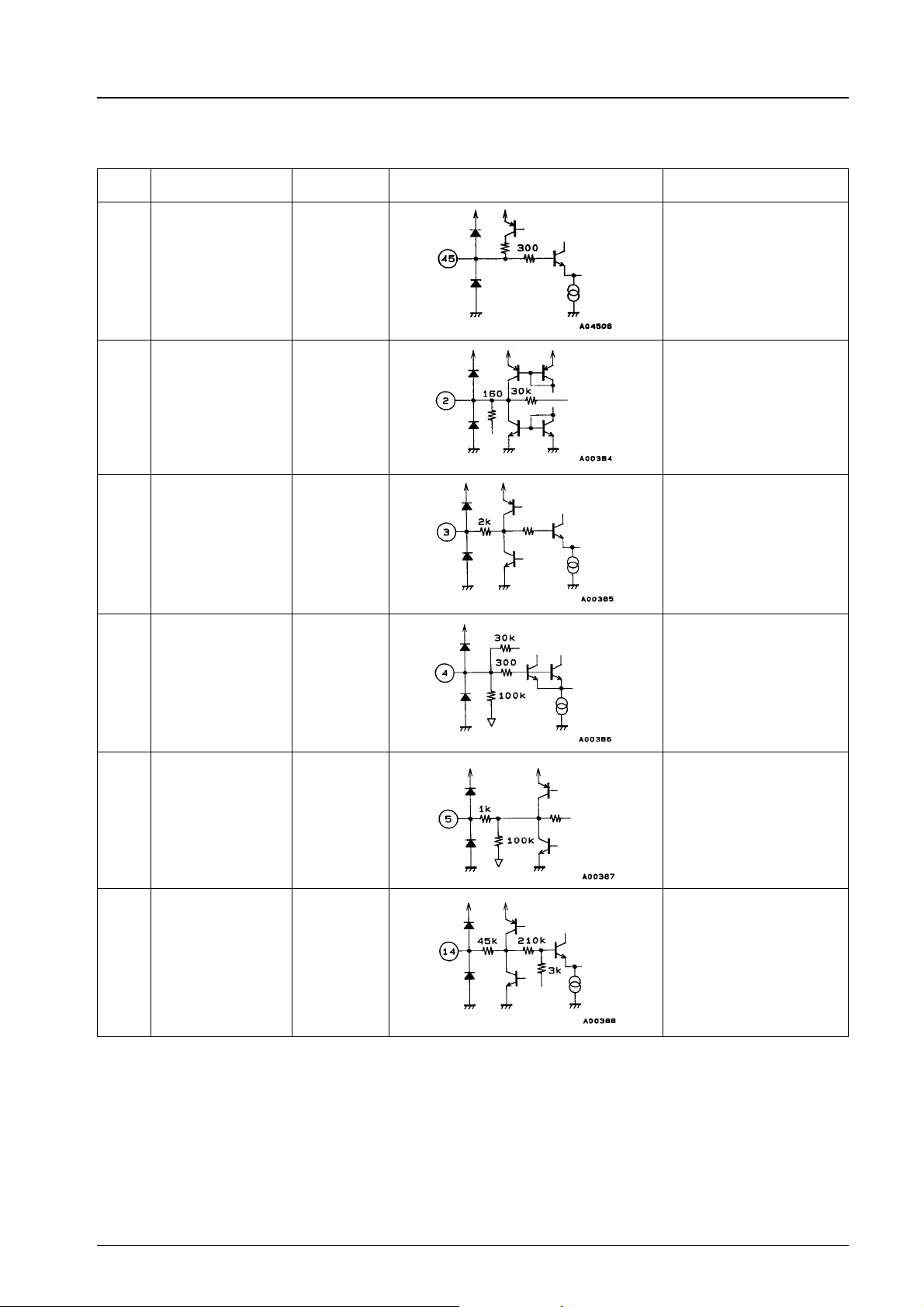
Pin Functions
Pin No. Pin name
45 R.F OUT 1.13
2
POWER OUT1
7
POWER OUTC
13
POWER OUT2
3
POWER NF REF1
9
POWER NF REFC
LA4587M
Unit (resistance:Ω, capacitance: F) * Pin voltage is when VCC= 1.2 V
Pin voltage
[V]
0.6 c A 160 Ω resistor is connected
0.75
Internal equivalent circuit Remarks
between individual outputs
(between pins 2 and 7, and
between pins 13 and 7).
c Each power NF connection
12
POWER NF REF2
4
POWER NF1
8
POWER NFC
11
POWER NF2
510POWER H.P1
POWER H.P2
14 L.P2 0.75
0.75
0.75
c Each power NF connection.
c Grounded to V
1kΩresistor when low boost
is on (pin 41: floating).
c Low boost secondary LP
connection.
REF
through a
Continued on next page.
No.5204-5/18

LA4587M
Continued from preceding page. Unit (resistance: Ω, capacitance: F)
Pin No. Pin name
15 Low Boost NF 0.75
Pin voltage
[V]
Internal equivalent circuit Remarks
c Low boost amplifier NF
connection.
1618POWER IN2
POWER IN1
17 L.P1 0.75
1920NFC2
NFC1
2128PRE NF1
PRE NF2
0.75
0.75
0.75 c Each preamplifier NF
c Each power input connection.
c The input resistance is
10 kΩ.
c An anti-buzz capacitor is built
in.
c Low boost primary LP.
connection.
connection.
c NF requires no capacitor.
2227PRE OUT1
PRE OUT2
0.45
c 200 kΩ is connected
between each output pin and
NF pin.
Continued on next page.
No.5204-6/18
 Loading...