

SANYO LA4581MB Datasheet

Ordering number: EN3535A
Monolithic Linear IC
LA4581MB
Preamplifier + Power Amplifier
for 3V Headphone Stereos
Overview
The LA4581MB is an auto reverse-supported preamplifier +
power amplifier IC that is intended for use in 3V headphone
stereos.
Features
.
Preamplifier muting and preamplifier output on/off can be
implemented with one pin. This IC can easily be used to
construct a set with a radio.
.
The power amplifier needs no input/output coupling
capacitor.
.
A high-frequency cut capacitor is connected to the
preamplifier input pin and the power amplifier input pin.
(Anti-buzz provision)
.
Because V
grounding impedance is about 10 Ω. This eliminates the
need for a large capacitor.
.
8 Ω speaker drivable.
AMP (r0=10Ω) is built in, the virtual
ref
Specifications
Maximum Ratings atTa=25°C
Package Dimensions
unit : mm
3112-MFP24S
[LA4581MB]
SANYO : MFP24S
Parameter Symbol Conditions Ratings Unit
Maximum supply voltage V
Allowable power dissipation Pd max 530 mW
Operating temperature Topr –20 to +75
Storage temperature Tstg –40 to +125
max 4.5 V
CC
Operating Conditions atTa=25°C
Parameter Symbol Conditions Ratings Unit
Recommended supply voltage V
Operating supply voltage range V
CC
op 1.8 to 3.6 V
CC
3.0 V
Operating Characteristics atTa=25°C, VCC=3.0V,f=1kHz, 0.775 V = 0 dBm,
=10kΩ(preamplifier), RL=16Ω(power amplifier)
R
L
Parameter Symbol
[Pre + Power]
Quiescent current I
Voltage gain (Closed) VG
CCO
Rg = 2.2 kΩ (preamplifer) VIN= 0 V 17 27 mA
VO= –5 dBm 65 68 71 dB
T
Output
min typ max Unit
Continued on next page.
SANYO Electric Co.,Ltd. Semiconductor Bussiness Headquarters
TOKYO OFFICE Tokyo Bldg., 1-10, 1 Chome, Ueno, Taito-ku, TOKYO, 110 JAPAN
22896HA(II) No.3535-1/8
C
°
C
°
Continued from preceding page.
LA4581MB
Parameter Symbol
Output
min typ max Unit
[Preamplifier]
Voltage gain (Open) VGo V
Voltage gain (Closed) VG1 V
Maximum output voltage V
max THD=1%,VCC= 1.8 V 0.1 0.2 V
O
Total harmonic distortion THD1 V
Equivalent input noise voltage V
1 Rg = 2.2 kΩ, B.P.F = 20 to 20 kHz 1.3 2.0 µV
N
= –5 dBm 70 80 dB
O
= –5 dBm 40 dB
O
= 0.2 V, VG = 40 dB/NAB 0.05 0.5 %
O
Crosstalk CT1 Rg = 2.2 kΩ, TUNE 1 kHz 60 80 dB
Ripple rejection ratio R
r
f = 100 Hz
Rg = 2.2 kΩ,V
1
= 1.8 V, Vr = –20 dBm,
CC
40 50 dB
[Power Amplifer]
Output voltage P
Voltage gain (Closed) VG2 V
Total harmonic distortion THD2 P
Interchannel crosstalk CT
Output noise voltage V
Ripple rejection ratio R
Input resistance R
DC offset voltage V
NO
r
IN
ODC
THD = 10% 23 32 mW
O
T
= –5 dBm 25 28 31 dB
O
= 1 mW 0.4 1.0 %
O
VO= –5 dBm, Rv=0Ω 30 40 dB
Rg = 0, B.P.F = 20 to 20 kHz 24 40 µV
2 Rg=0,Vr= –20 dB, f = 100 Hz, VCC= 1.8 V 45 60 dB
22 30 38 kΩ
off Between 13-14 and 15 –90 +90 mV
Note) Power amplifier voltage gain VG2 increases by about 1 dB for min/max respectively than specified above when RL=32Ω.
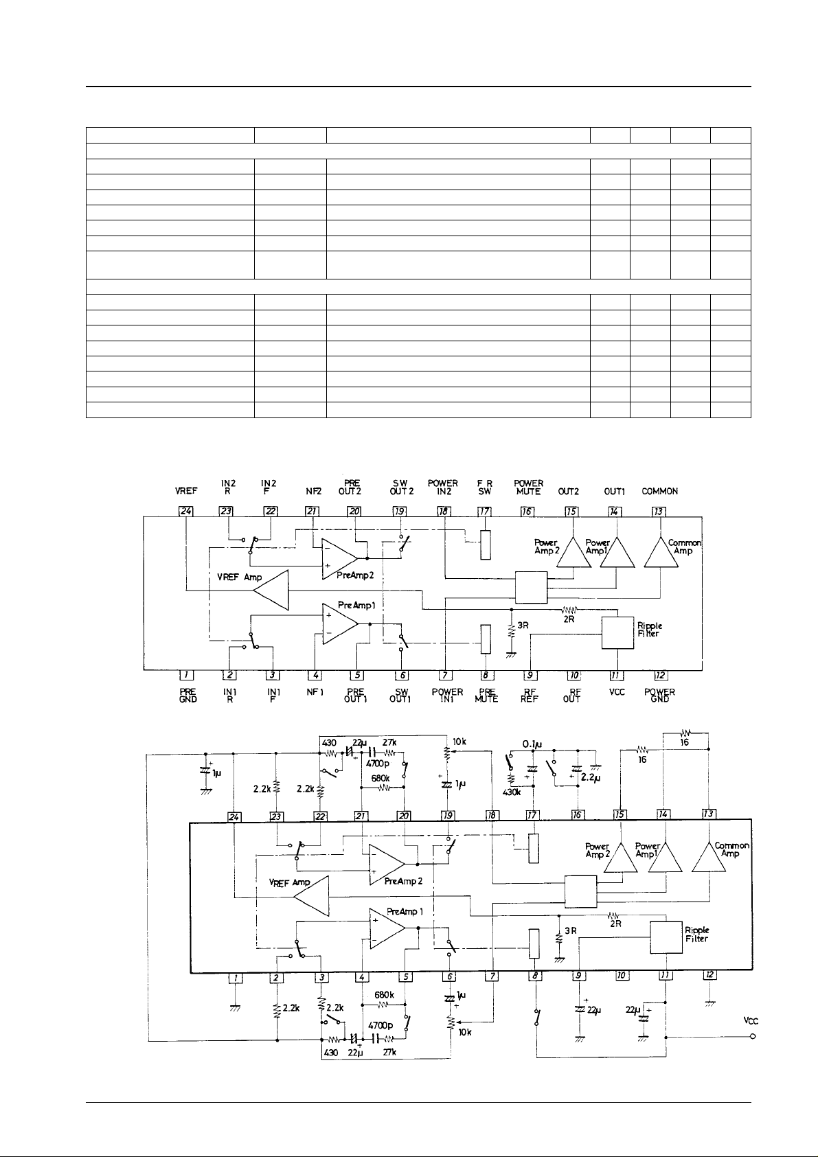
Block Diagram
Test Circuit
1.8 to 3.0 V
Unit (resistance: Ω, capacitance: F)
No.3535-2/8
LA4581MB
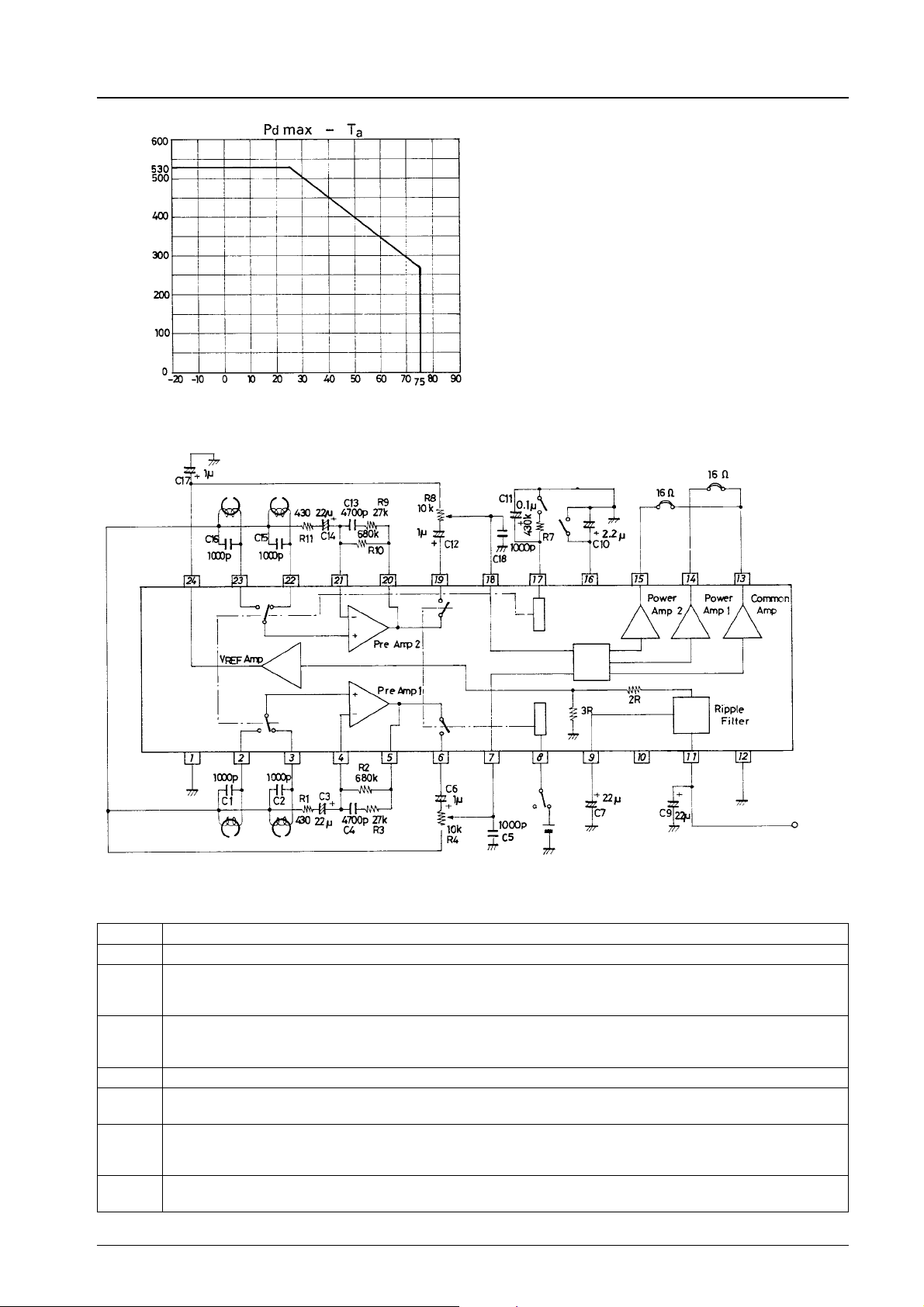
Allowable power dissipation, Pd max − mW
Ambient temperature, Ta −°C
Sample Application Circuit
Note) Pre closed loop gain VG = 40 dB/1 kHz NAB
Preamplifier input is applied to pins 2,23/
pins 3,22 when SW ON/OFF, respectively.
PRE MUTE ON when
connected to V
POWER MUTE ON when
connected to GND.
1.8 to 3.6 V
CC
Unit (resistance: Ω, capacitance: F)
Pin and external part functions (when the voltage is V
Pin No. Pin Function
1 PRE GND
PRE IN1R 1.8 V
2
v Turns ON when pin 17 is grounded.
v A bias resistor (2.2 kΩ) must be connected between pin 2 and pin 24 (V
PRE IN1F 1.8 V
3
v Turns ON when pin 17 is floating.
v A bias resistor (2.2 kΩ) must be connected between pin 3 and pin 24 (V
4 PRE NF1 1.8 V
PRE OUT1 1.8 V
5
v Like pin 6, 10 kΩ load drivable.
SW OUT1 1.8V
6
v Provides PRE AMP1 output when pin 8 is floating (PRE MUTE OFF)(equivalent to pin 5).
v Disconnects from PRE AMP1 and sets R
POWER IN1 1.8V
7
v Input resistance R
7 30 kΩ
IN
^ 500 kΩ when pin 8 is at VCC(PRE MUTE ON).
IN
= 3.0 V)
CC
) when no head is in use.
ref
) when no head is in use.
ref
Continued on next page.
No.3535-3/8
 Loading...