

SANYO LA4536M Datasheet
Any and all SANYO products described or contained herein do not have specifications that can handle
applications that require extremely high levels of reliability, such as life-support systems, aircraft’s
control systems, or other applications whose failure can be reasonably expected to result in serious
physical and/or material damage. Consult with your SANYO representative nearest you before using
any SANYO products described or contained herein in such applications.
SANYO assumes no responsibility for equipment failures that result from using products at values that
exceed, even momentarily, rated values (such as maximum ratings, operating condition ranges,or other
parameters) listed in products specifications of any and all SANYO products described or contained
herein.
Monolithic Linear IC
5V CD Headphone-stereo Power Amplifier
Ordering number:ENN4033A
LA4536M
SANYO Electric Co.,Ltd. Semiconductor Company
TOKYO OFFICE Tokyo Bldg., 1-10, 1 Chome, Ueno, Taito-ku, TOKYO, 110-8534 JAPAN
The LA4536M is a low noise, low distortion headphonestereo power IC designed for use on a portable CD.
Features
• Less current drain.
• Accept 16Ω load drive.
• Excellent voltage reduction characteristic.
• Excellent ripple rejection.
• Power switch function and built-in muting circuit.
• Low noise (7µV), low gain (11dB).
Specifications
Absolute Maximum Ratings at Ta = 25˚C
retemaraPlobmySsnoitidnoCsgnitaRtinU
egatlovylppusmumixaMV
noitapissidrewopelbawollAxamdP 003Wm
erutarepmetgnitarepOrpoT 57+ot02–
erutarepmetegarotSgtsT 521+ot04–
xamlangisoN 0.6V
CC
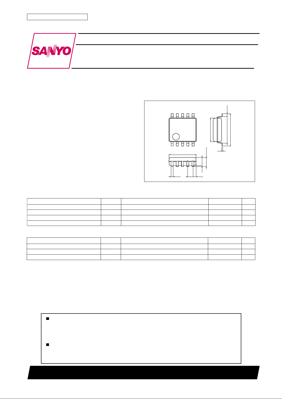
Package Dimensions
unit:mm
3086A-MFP10S
[LA4536M]
10
1
6
5
5.1
0.55
1.00.35
1.5˚
0.1
1.8max
4.4
0.15
SANYO : MFP10S
0.625
5.15
6.4
˚C
˚C
Operating Characteristics at Ta = 25˚C
retemaraPlobmySsnoitidnoCsgnitaRtinU
egatlovylppusdednemmoceRV
egnaregatlovylppusgnitarepOV
ecnadepmidaoldednemmoceRR
CC
poCC
L
O3098HA (KT)/62598RM (KI) No.4033–1/9
0.5V
0.6ot0.4V
23ot61 Ω
LA4536M
Operating Characteristics at Ta = 25˚C, RL=16Ω, Rg=600Ω
retemaraPlobmySsnoitidnoC
I
1V
tnerructnecseiuQ
niagegatloVGVV
snoitairavniagegatloV
noitrotsidcinomrahlatoTDHTV
rewoptuptuOP
klatssorCTC
noitcejerelppRRRVS
egatlovesiontuptuOV
tceffefforewoPV
tceffeetuMV
ytivitisnestnerrucnorewoP1I
ytivitisnesegatlovfforewoP)ffo(1V5.06.0V
ytivitisnestnerrucffoetuM)ffo(01I2.00.2Aµ
ytivitisnesegatlovnoetuM)no(01V5.056.0V
I
I
∆VG1
∆VG2
OCC
OCC
OCC
O
ON
CC
2V
CC
3V
CC
CC
V
CC
V
CC
CC
V
CC
V
CC
V
O
V
CC
V
O
V
CC
V
CC
)ffo(O
V
NI
V
CC
)TM(O
V
NI
VCC=5.0V, V5≥0.85V
)no(
VCC=5.0V, V5≤0.1V
VCC=5.0V, V5 ≥0.85V
VCC=5.0V, V5≤0.1V
langison,V0.5=0.102Am
DNG,01nip,V0.6=1.10.4Am
DNG,1nip,V0.6=0.1Aµ
V,zHk1=f,V0.5=
V,zHk1=f,V0.5=
V,zHk1=f,V0.4=
P,zHk1=f,V0.5=
mBd01–=
k1=gR,V0.6= Ω,
zH02otzH02=FPB
mBd01–=
mBd01–=
mBd01–=91131Bd
O
mBd01–=0.1Bd
O
mBd02–=0.1Bd
O
Wm1=20.042.0%
O
%01=DHT,zHk1=f,V0.5=04001Wm
k1=gR,zHk1=f,V0.5= Ω,
k1=gR,zH001=f,V0.4= Ω,
zH001=FPB,mBd02–=
,DNGot1niP,zH001=f,V0.4=
,DNGot1niP,zH001=f,V0.4=
nimpytxam
0406Bd
5456Bd
*1 : Quiescent current is the current flowing into pin 6. The current flowing into pin 1 and pin 10 is at the maximum value and calculated from
the equation (V pin–0.5V)/16[V/kΩ], increasing total current.
sgnitaR
702Vµ
08– mBd
08– mBd
50.00.2Aµ
tinUetoN
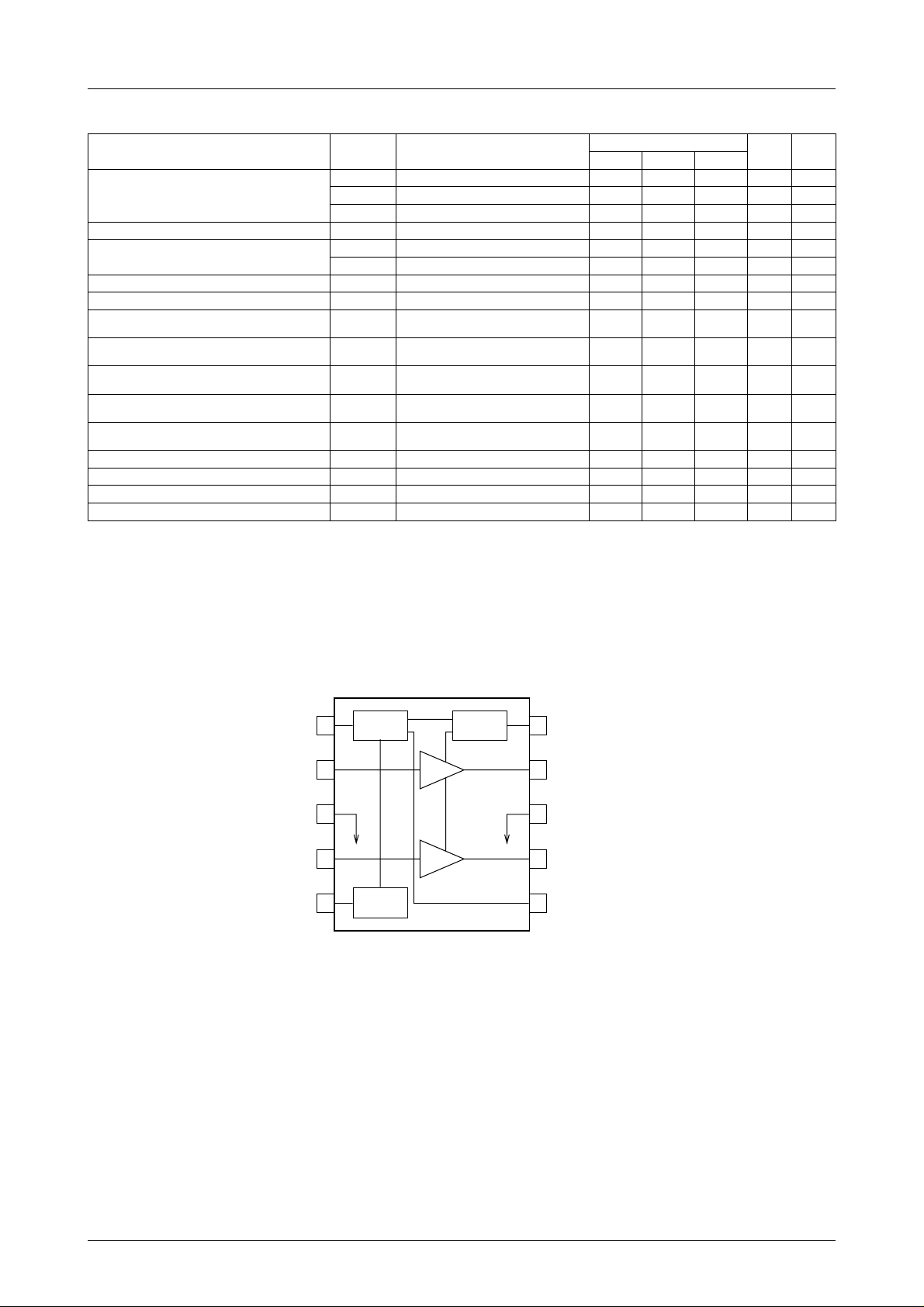
Equivalent Circuit Block Diagram
P/SW
IN 1
PRE GND
IN 2
REF
POWER
1
SWITCH
2
3
4
5
BIAS
Amp1
Amp2
MUTE
CIRCUIT
10
MT/SW
9
OUT 1
POWER GND
8
OUT 2
7
6
V
CC
A11160
No.4033–2/9
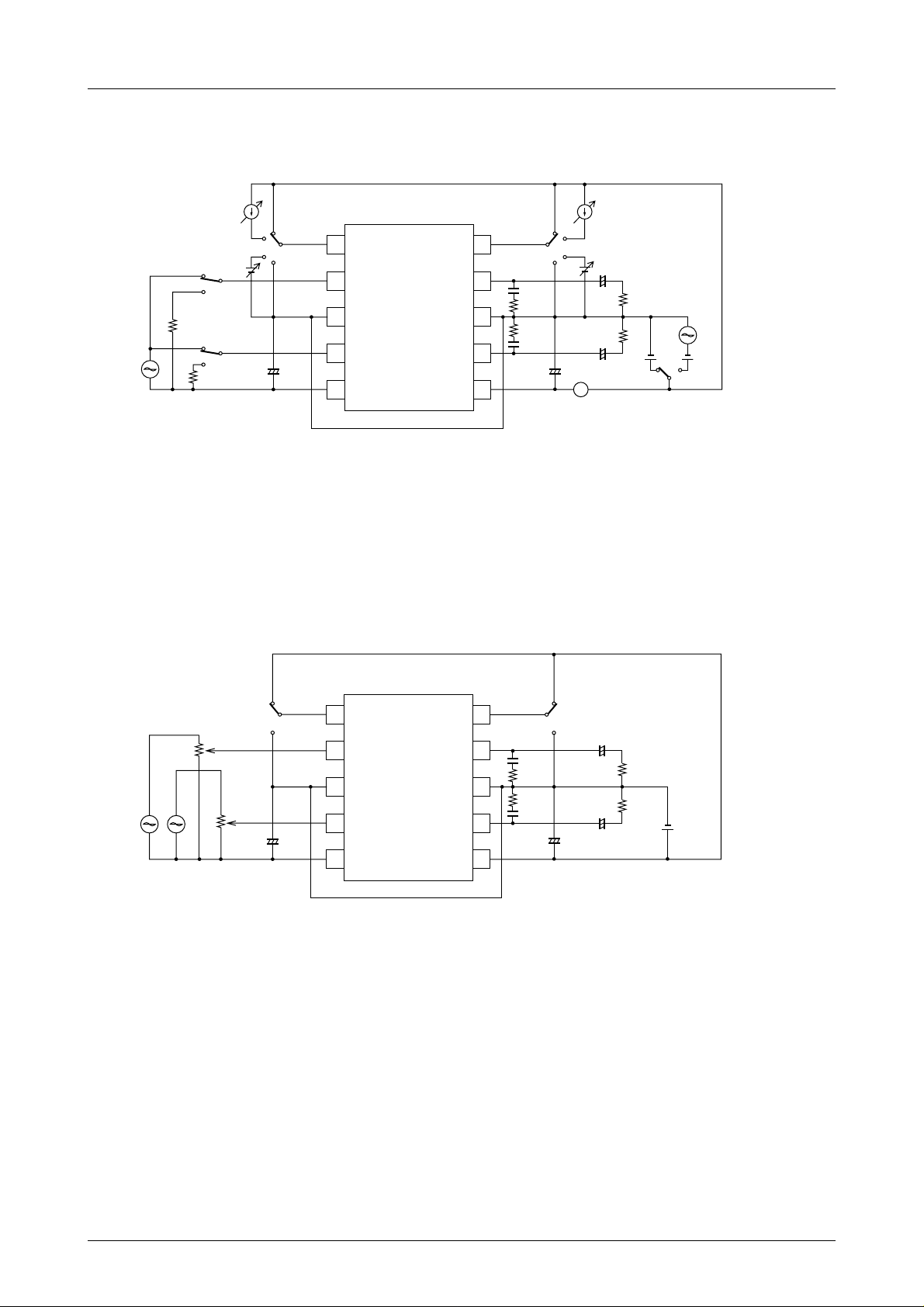
Test Circuit
LA4536M
I
1
2
3
V
1
1
2
Rg
1kΩ
1
2
SG
22µF 4.7µF
Rg
1kΩ
+
Sample Application Circuit
1
P/SW MT/SW
4
P/SW
1
IN 1
2
PRE
GND
IN 2
REF
LA4536M
3
4
5
MT/SW
OUT 1
POWER
GND
OUT 2
V
CC
10
9
8
7
6
0.1µF
2.2Ω
2.2Ω
0.1µF
I
10
1
2
3
V
4
+
10
220µF
+
R
L
16Ω
R
L
16Ω
+
220µF
A
I
CC
V
V
CC
DC RIPPLE
R
A11161
SG
0.1µF
2.2Ω
2.2Ω
0.1µF
OFF
ON
+
+
+
220µF
220µF
R
16Ω
R
16Ω
L
L
–
V
CC
+
A11162
ON
P/SW MT/SW
OFF
V
R
V
R
SG
1
2
22µF 4.7µF
+
P/SW
1
IN 1
2
PRE
LA4536M
3
GND
4
IN 2
5
REF
MT/SW
OUT 1
POWER
GND
OUT 2
V
CC
10
9
8
7
6
No.4033–3/9
 Loading...