SANYO LA4425A Datasheet

Ordering number: EN3309C
Monolithic Linear IC
LA4425A
5 W Power Amplifier with Very Few External Parts
for Car Radio and Car Stereo
Features
.
The world’s first power amplifier with very few external
parts.
The smallest package in the industry
→ [SIP-5H (TO-126 type)]
Only two external parts
→ [Only I/O coupling capacitors]
.
Almost no evaluation, adjustment and check of its functions
as a power IC required
→ [Simplified control]
.
Wide operation supply range → 5to16V
.
On-chip protection:
Overvoltage protection
Thermal protection
Output D.C. short protection
.
On-chip pop noise reducing circuit
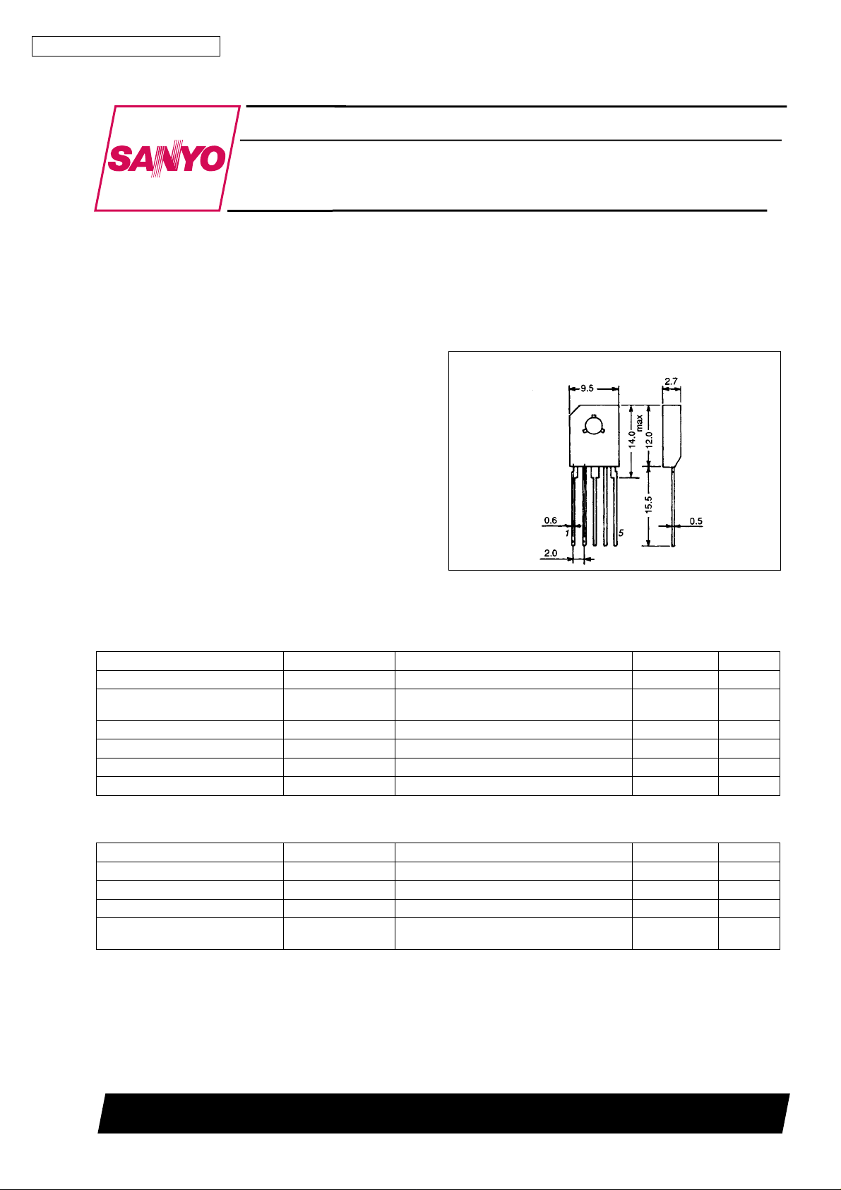
Package Dimensions
unit : mm
3031A-SIP-5H
[LA4425A]
SANYO : SIP5H
Specifications
Maximum Ratings at Ta = 25°C
Parameter Symbol Conditions Ratings Unit
Maximum supply voltage V
Surge maximum supply voltage V
Maximum output current I
Allowable power dissipation Pd max With infinite heat sink 7.5 W
Operating temperature Topr –30 to +80 °C
Storage temperature Tstg –40 to +150 °C
max Rg = 0 18 V
CC
surge
CC
peak 3.3 A
O
Giant pulse 200 msec
Rise time 1 ms
50 V
Operating Conditions at Ta = 25°C
Parameter Symbol Conditions Ratings Unit
Recommended supply voltage V
Recommended load resistance R
Operating voltage range V
Operating load resistance range R
CC
L
op 5to16 V
CC
op
L
Under conditions where maximum ratings
are not exceeded
SANYO Electric Co.,Ltd. Semiconductor Bussiness Headquarters
TOKYO OFFICE Tokyo Bldg., 1-10, 1 Chome, Ueno, Taito-ku, TOKYO, 110 JAPAN
53096HA(II)/20293TS/9200TA,TS(KOTO)/3050TA,TS(AF) No.3309-1/8
13.2 V
4 Ω
2to8 Ω

LA4425A
Operating Characteristics at Ta = 25°C, VCC= 13.2 V, RL=4Ω,f=1kHz, Rg = 600 Ω, specified
3
board/specified circuit, 30 × 30 × 1.5 mm
Parameter Symbol Conditions min typ max Unit
Quiescent current I
Voltage gain VG V
Output power
Total harmonic distortion THD V
Output noise voltage V
Ripple rejection ratio
Overvoltage attack V
Starting time t
Input resistance R
Roll-off frequency
Thermal operating temperature Tc 125 °C
CCO
P
1 13.2 V/4 Ω, THD = 10% 4 5 W
O
P
2 14.4 V/4 Ω, THD = 10% 5 6 W
O
NO
SVRR
1
SVRR
2
CCX
s
IN
f
L
f
H
= 0 dBm 43 45 47 dB
O
= 2V 0.1 1.0 %
O
Rg = 0, BPF = 20 Hz to 20 kHz 0.15 0.5 mV
Rg=0,BPF=20Hzto20kHz
V
= 0 dBm, fR= 100 Hz
R
Rg=0,BPF=20Hzto20kHz
V
= 0 dBm, fR= 1 kHz
R
Rg = 0 21.5 V
thick aluminum used
65 130 mA
30 40 dB
47 dB
0.35 s
50 kΩ
40 Hz
90 kHz
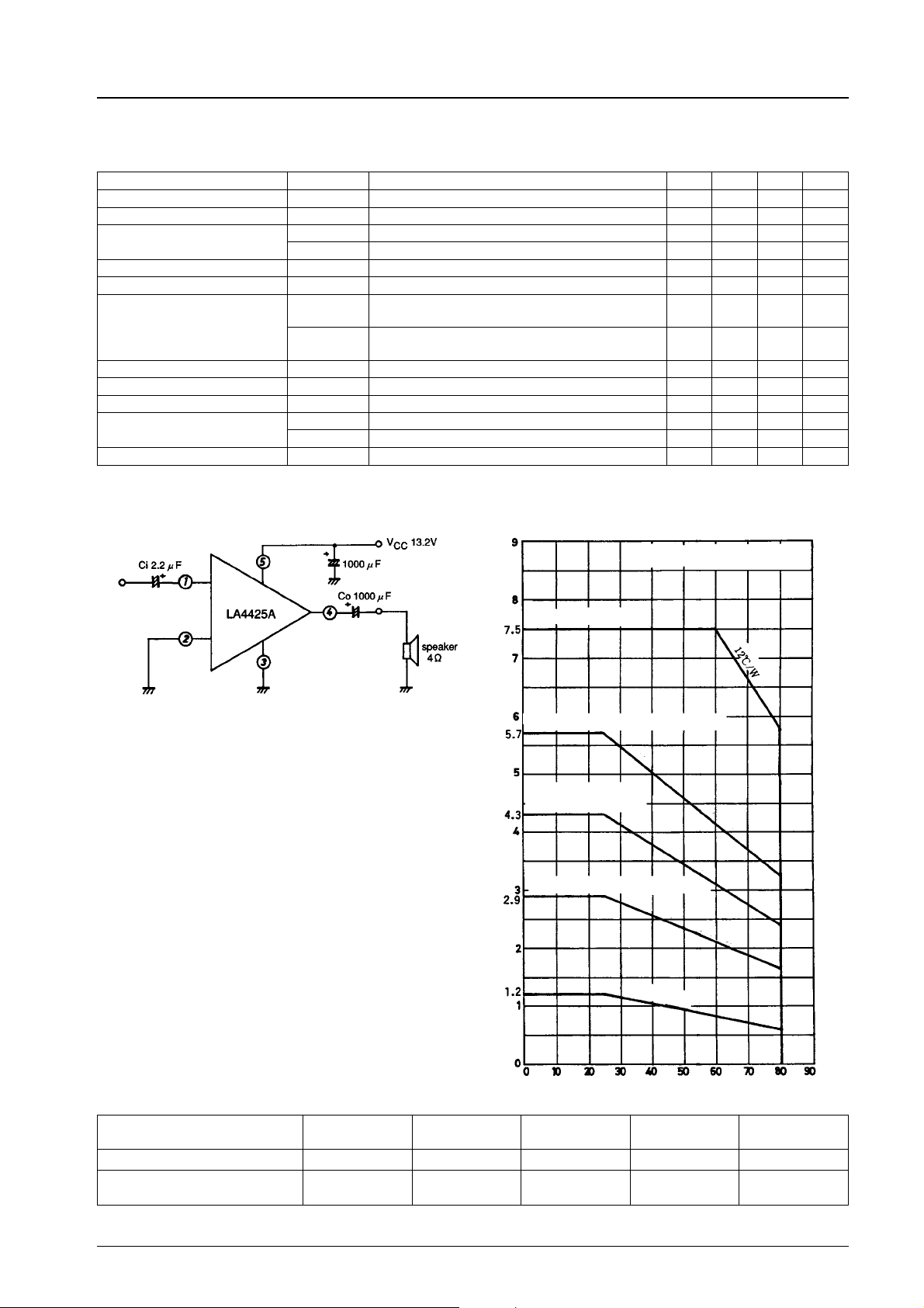
Sample Application Circuit
Pd max – Ta
With silicone grease applied.
Heat sink mounting torque 39 N·cm
.
On-chip overvoltage protection
.
On-chip thermal protection
.
On-chip pop noise reducing circuit
.
On-chip output D.C. short protection
With infinite heat sink
With 100 × 100 × 1.5 mm
With 50 × 50 × 1.5 mm
Al heat sink
With 30 × 30 × 1.5 mm
Allowable Power Dissipation, Pd max – W
3
Al heat sink
3
3
Al heat sink
No heat sink
Pin Voltage at VCC= 13.2 V
Characteristics Input
PinNo. 12345
Pin voltage
(reference value)
(6 2V
1.4 V
BE
Ambient temperature, Ta – °C
Small signal
GND
)
0V 0V
Large signal
GND
Output V
(6 1/2 VCC)
6.5 V
CC
(VCC)
13.2 V
No.3309-2/8

LA4425A
IC Usage Notes
Maximum ratings
If the IC is used in the vicinity of the maximum ratings, even a slight variation in conditions may cause the maximum ratings to
be exceeded, thereby leading to a breakdown.
Printed circuit board
When drawing the printed circuit pattern, refer to the sample printed circuit pattern. Be careful not to form a feedback loop
between input and output.
Comparison of External Components
External Parts Our ICs now in use LA4425A
Output coupling capacitor jj
Input coupling capacitor jj
Bootstrap capacitor j —
Feedback capacitor j —
Filter capacitor j —
Phase compensation capacitor j —
Oscillation correction polyester
film capacitor
Oscillation correction resistor j —
Total 8 pcs. 2 pcs.
j —
Note: The power supply capacitor is not counted as a power IC part.
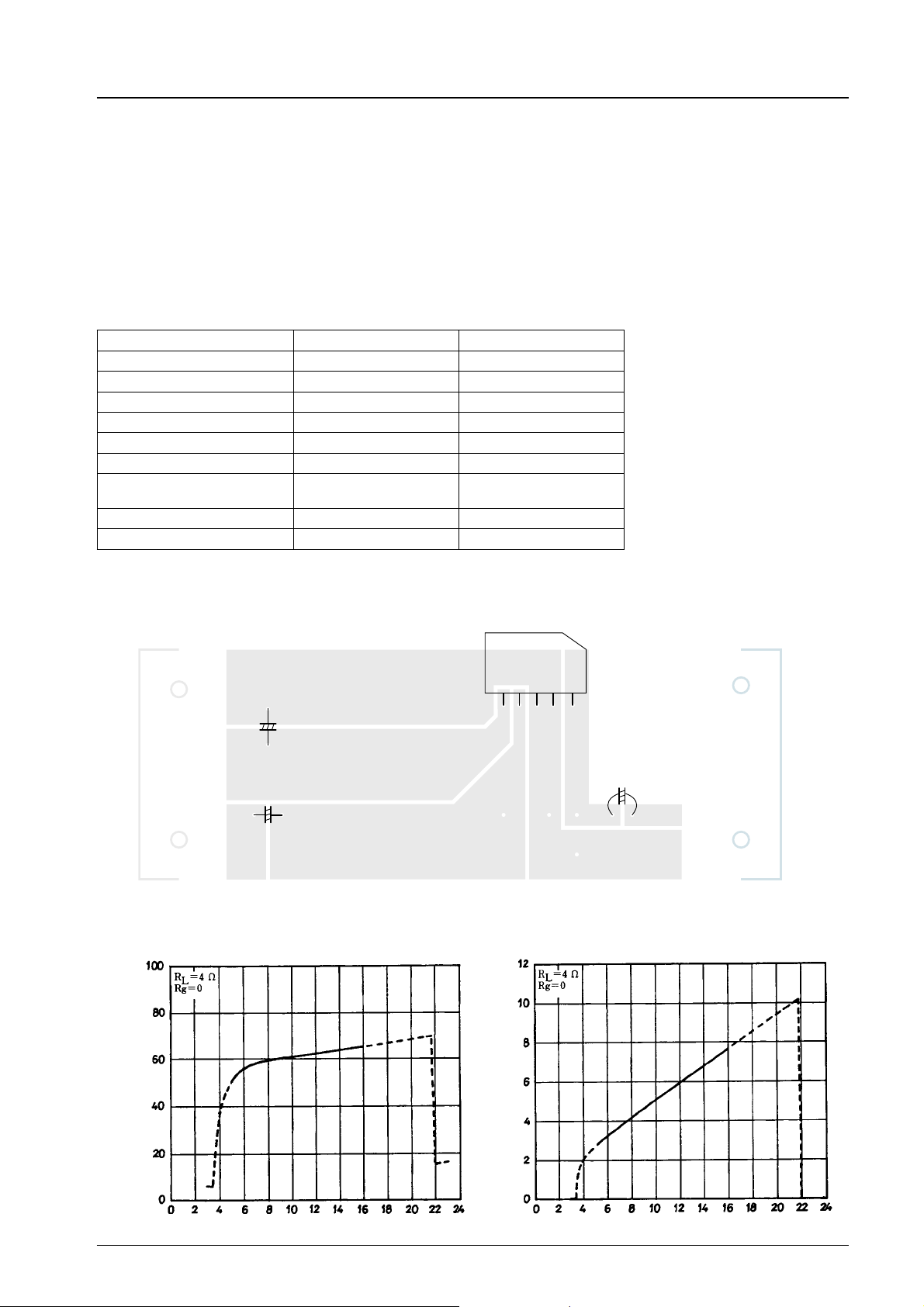
Sample Printed Circuit Pattern
–mA
CCO
GND
V
CC
OUT Co = 1000 µF
= 1000 µF
CV
CC
–
+
+–
I
CCO–VCC
LA4425A
+
–
Ci = 2.2 µF GND
Cu-foiled side 78.0 × 29.0 mm
VN–V
–V
N
IN
2
CC
Quiescent current, I
Supply voltage, VCC–V
Output pin voltage, V
Supply voltage, VCC–V
No.3309-3/8
 Loading...