

SANYO LA2000M Datasheet

Ordering number: EN4158
Monolithic Linear IC
LA2000M
Audio Level Sensor
Overview
LA2000M is an IC for detecting interprogram spaces to pick
out the starting point of a program immediately preceding or
following a musical program recorded on tape, and to detect
end of tape.
Used in
.
Radio-cassette recorders
.
Cassette decks
.
Car stereos
Applications
.
Detection of spaces between programs recorded on tape
.
Detection of end of tape
.
Other
Features
.
Has transistors capable of driving plungers with maximum
50 mA, and a protective diode to prevent induced reverse
voltages.
.
Can provide designated time delays by externally connected
capacitors and resistors.
.
Has a comparator with stable hysteresis to handle variations
in power supply voltage.
.
Detects unrecorded portions of tape.
Package Dimensions
unit : mm
3032B-MFP8
[LA2000M]
SANYO : MFP8
Specifications
Maximum Ratings at Ta = 25°C
Parameter Symbol Conditions Ratings Unit
Maximum supply voltage V
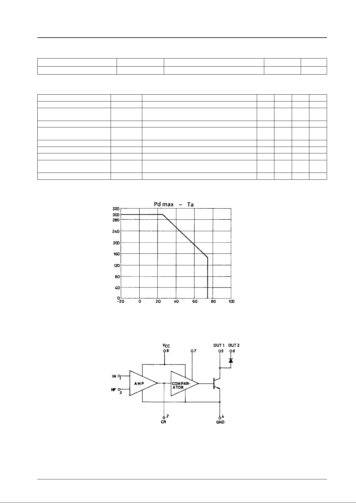
Allowable power dissipation Pd max 300 mW
Flow-in current I
Operating temperature Topr −20 to +75 °C
Storage temperature Tstg −40 to +125 °C
Note:1. The voltage at pin 7 must not exceed the supply voltage at pin 8.
2. The maximum current flowing into pin 7 should be no greater than 0.5 mA.
max 15 V
CC
max 50 mA
6
SANYO Electric Co.,Ltd. Semiconductor Bussiness Headquarters
TOKYO OFFICE Tokyo Bldg., 1-10, 1 Chome, Ueno, Taito-ku, TOKYO, 110 JAPAN
42896HA(II) No. 4158-1/7
LA2000M
Operating Conditions at Ta = 25°C
Parameter Symbol Conditions Ratings Unit
Operating supply voltage V
Operating Characteristics at Ta = 25°C, VCC=9.0V,f=1kHz
Parameter Symbol Conditions min typ max Unit
Circuit current I
Output transistor saturating
voltage
Output diode forward voltage V
Output-off level in input
equivalent
Comparator-on level V
Comparator-off level V
Pin 7 high level V
Output transistor leakage
current
Output diode leakage current I
CC
V
CE (sat)I6
V
TH-H
TH-L
7
I
L-TR
L-Di
op 3.5 to 14 V
CC
f = 1 kHz, VIN= −45 dBm 6 12 mA
= 50 mA 0.5 1.8 V
IF= 50 mA 0.7 1.5 V
F
IN
f = 1 kHz −43 −50 −54 dBm
pin 0.45 0.55 V
3.0 3.5 4.0 V
1.8 2.2 2.6 V
100 µA
100 µA
Allowable power dissipation, Pd max − mW
Equivalent Circuit Block Diagram
Ambient temperature, Ta − °C
No.4158-2/7
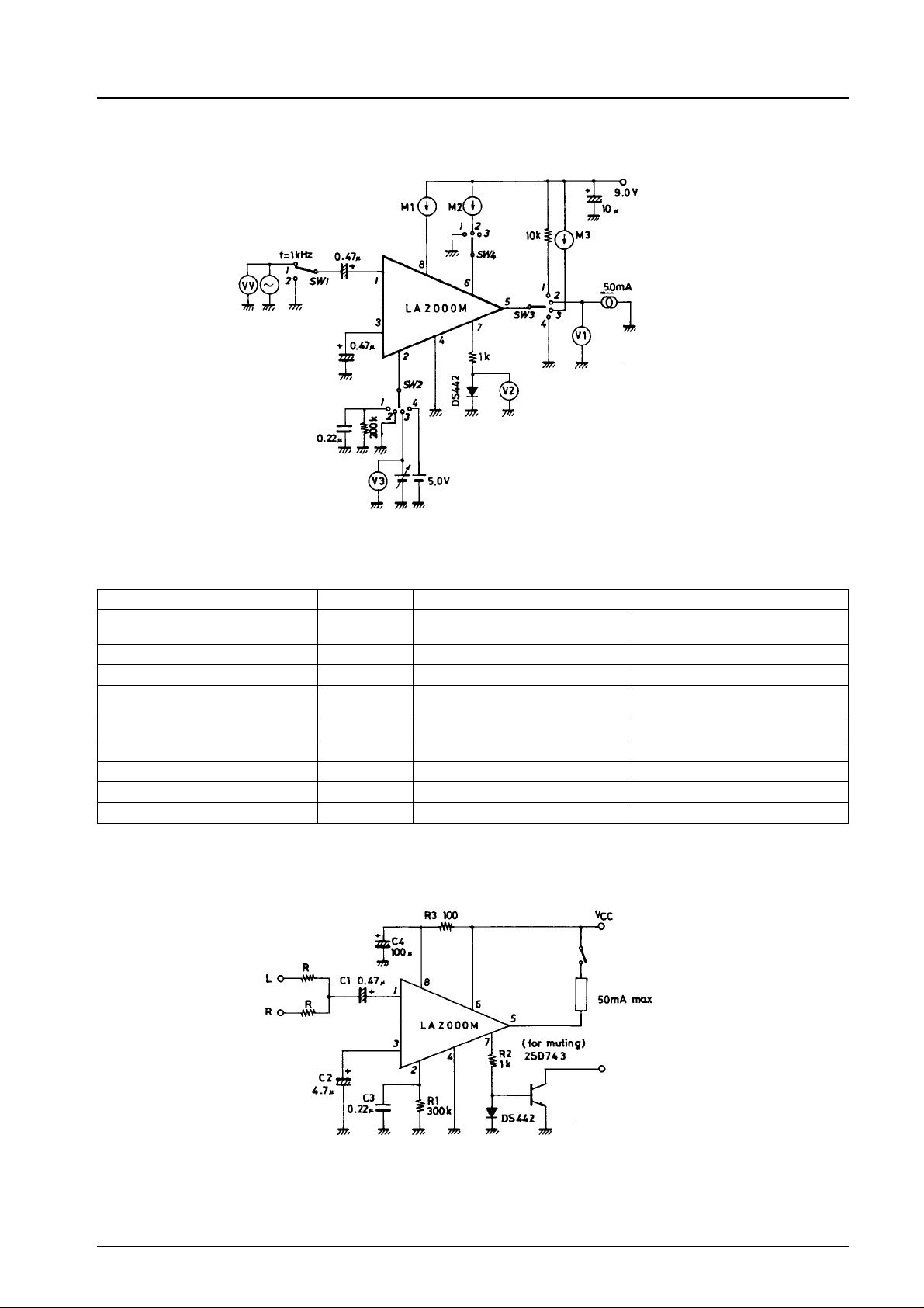
Test Circuit
LA2000M
Unit (resistance: Ω, capacitance: F)
Test Conditions
Test items Symbol SW-1 SW-2 SW-3 SW-4 Conditions
Circuit current I
Output transistor saturation voltage V
Output diode forward voltage V
Output-off level in input equivalent V
Comparator-on level V
Comparator-off level V
Pin 7 high level Vp-7 2413Measure V
Output transistor leakage current I
Output diode leakage current I
CC
CE (sat)
F
IN
H
L
TL
DL
1113Measure current flowing into pin 8 at
2223Measure VINat pin 5
2421Measure VINat pin 5
1113Input level (v.v) when pin 5 turns
2313Measure V3when pin 5 turns over
2313Measure V3when pin 5 turns over
2433Measure M3
2442Measure M2
V
IN
over
= −45 dB
Sample Application Circuit 1
Mechanism-coupled switch
(OFF at play mode)
Plunger
at pin 7
2
Unit (resistance: Ω, capacitance: F)
No.4158-3/7
 Loading...