

Page 1

Any and all SANYO products described or contained herein do not have specifications that can handle
applications that require extremely high levels of reliability, such as life-support systems, aircraft’s
control systems, or other applications whose failure can be reasonably expected to result in serious
physical and/or material damage. Consult with your SANYO representative nearest you before using
any SANYO products described or contained herein in such applications.
SANYO assumes no responsibility for equipment failures that result from using products at values that
exceed, even momentarily, rated values (such as maximum ratings, operating condition ranges,or other
parameters) listed in products specifications of any and all SANYO products described or contained
herein.
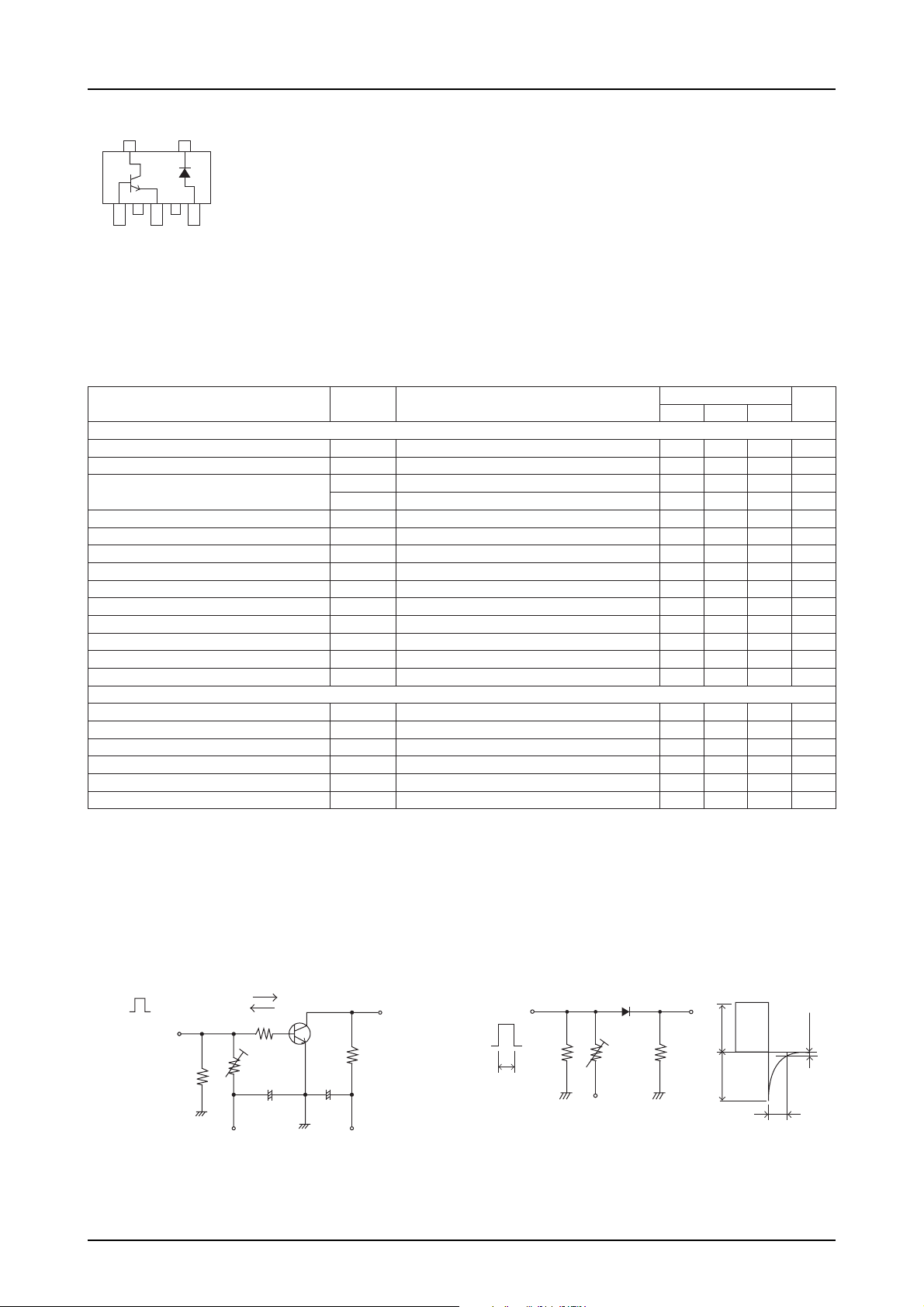
TR:NPN Epitaxial Planar Silicon Transistor
SBD:Schottky Barrier Diode
DC-DC Converter Applications
Ordering number:ENN4657
FP303
SANYO Electric Co.,Ltd. Semiconductor Company
TOKYO OFFICE Tokyo Bldg., 1-10, 1 Chome, Ueno, Taito-ku, TOKYO, 110-8534 JAPAN
4.5
4.25max
Features
· Composite type with NPN transistor and Schottoky
barrier diode facilitates high-density mounting.
· The FP303 is composed of chips equivalent to the
2SD1623 and SB05-05CP, which are placed in one
package.
Specifications
Absolute Maximum Ratings at Ta = 25˚C
retemaraPlobmySsnoitidnoCsgnitaRtinU
]RT[
egatloVesaB-ot-rotcelloCV
egatloVrettimE-ot-rotcelloCV
egatloVesaB-ot-rettimEV
tnerruCrotcelloCI
)esluP(tnerruCrotcelloCI
tnerruCesaBI
noitapissiDrotcelloCP
erutarepmeTnoitcnuJjT 051
erutarepmeTegarotSgtsT 051+ot55–
]DBS[
egatloVesreveRkaePevititepeRV
egatloVegruSesreveRkaePevititeper-noNV
tnerruCdeifitceRegarevAI
tnerruCdrawroFegruSI
erutarepmeTnoitcnuJjT 521+ot55–
erutarepmeTegarotSgtsT 521+ot55–
OBC
OEC
OBE
C
PC
B
C
MRR
MSR
O
MSF
Package Dimensions
unit:mm
2099A
3.4
2.8
0.5
1.8
0.5
6
1.0
2.5
1.0
4
5
3
1.75
3.5
Mounted on ceramic board (250mm
elcyc1,evaweniszH05 5A
0.5
7
2
1
1.75
1.2
2
×0.8mm)
[FP303]
1.5
0.4
1.57
0.5
0.2min
0.3
0 to 0.1
0.2
1:Base
2:Collector
3:Emitter
4:Cathode
5:Anode
6:Cathode
7:Collector
0.7
SANYO:PCP5
(Bottom view)
06V
05V
6V
2A
4A
004Am
8.0W
˚C
˚C
05V
55V
005Am
˚C
˚C
72701TN(KT)/52098HA (KT)/N2394TS (KOTO) B8-0025 No.4657-1/5
Page 2
FP303
Electrical Connection
7
24
13
6
5
Electrical Characteristics at Ta=25˚C
]RT[
tnerruCffotuCrettimEI
niaGtnerruCCD
ecnaticapaCtuptuOboCV
emiTNO-nruTt
emiTegarotSt
emiTllaFt
]DBS[
egatloVesreveRV
egatloVdrawroFV
tnerruCesreveRI
ecnatsiseRlamrehTa-jhtR 071
1:Base
2:Collector
3:Emitter Common
4:Cathode
5:Anode
6:Cathode
7:Collector
(Top View)
retemaraPlobmySsnotidnoC
tnerruCffotuCrotcelloCI
hEF1VECI,V2=
hEF2VECI,V2=
tcudorPhtdiwdnaB-niaGf
egatloVnoitarutaSE-CV
egatloVnoitarutaSE-BV
egatloVnwodkaerBB-CV
egatloVnwodkaerBE-CV
egatloVnwodkaerBB-EV
ecnaticapaClanimretretnICV
emiTyrevoceResreveRt
V
OBC
V
OBE
V
T
I
)tas(EC
C
I
)tas(EB
C
I
OBC)RB(
C
I
OEC)RB(
C
I
OBE)RB(
E
no
gts
f
I
R
R
I
F
F
VRV52= 05Aµ
R
R
IFI=
rr
Mounted on ceramic board (250mm2×0.8mm)
I,V05=
BC
BE
EC
EC
R
0=1.0Aµ
E
I,V4=
0=1.0Aµ
C
Am001=041065
C
A5.1=04
C
I,V01=
Am05=
C
zHM1=f,V01=
I,A0.1=
Am05=
B
I,A0.1=
Am05=9.02.1V
B
I,Aµ01=
0=06V
E
R,Am1=
=∞ 05V
EB
I,Aµ01=
0=6V
C
Aµ002=05V
Am005= 55.0V
tiucriCtseTdeificepseeS06sn
tiucriCtseTdeificepseeS055sn
tiucriCtseTdeificepseeS03sn
zHM1=f,V01=22Fp
sgnitaR
nimpytxam
051zHM
21Fp
51.04.0V
.tiucriCtseTdeificpeseeS,Am001= 01sn
˚C/W
tinU
Marking:303
Switching Time Test Circuit
[TR]
I
V
R
B1
I
B2
R
B
+
100µF 470µF
PW=20µs
D.C.≤1%
INPUT
50Ω
10IB1= --10IB2=IC=500mA
[SBD]
OUTPUT
R
L
50Ω
+
VCC=25VVBE= --5V
Duty≤10%
10µs
50Ω 100Ω 10Ω
--5V
100mA100mA
10mA
t
rr
No.4657-2/5
Page 3

2.4
2.0
–A
1.6
C
50mA
10mA
20mA
I
C
-- V
CE
[TR]
FP303
–A
C
1.2
1.0
0.8
7mA
I
C
6mA
-- V
5mA
CE
4mA
[TR]
1.2
8mA
6mA
0.8
Collector Current, I
0.4
0
0 0.4 0.8 1.2 1.6 2.0 2.4
4mA
2mA
IB=0
Collector-to-Emitter Voltage, VCE–V
I
-- V
2.4
2.0
–A
1.6
C
1.2
0.8
C
Collector Current, I
0.4
0
0 0.2 0.4 0.6 0.8 1.21.0
BE
°C
Ta=75
25°C
--25°C
Base-to-Emitter Voltage, VBE–V
f
-- I
T
1000
– MHz
T
100
7
5
3
2
7
5
C
ITR11096
[TR]
VCE=2V
ITR11098
[TR]
VCB=10V
0.6
3mA
2mA
0.4
Collector Current, I
0.2
0
024681012
Collector-to-Emitter Voltage, VCE–V
h
-- I
25°C
--25
FE
°C
1000
7
5
3
FE
2
100
7
DC Current Gain,h
5
3
2
57 723 5723 5 23
Ta=75°C
0.01 1.00.1
C
Collector Current, IC–A
100
Cob -- V
7
5
3
2
CB
1mA
IB=0
ITR11097
VCE=2V
ITR11099
f=1MHz
[TR]
[TR]
3
2
Gain-Bandwidth Product, f
10
1000
23 57
10 100
7
5
–mV
3
2
CE(sat)
100
7
5
3
2
Collector-to-Emitter
Saturation Voltage, V
10
775532753232
0.01 0.1 1.0
Collector Current, IC–mA
23 57 23
VCE(sat) -- I
°C
25
Ta=75°C
°C
--25
Collector Current, IC–A
C
1000
ITR11100
IC / IB=20
ITR11102
[TR]
10
Output Capacitance, Cob – pF
7
5
1.0
10
7
5
(sat) – V
3
BE
2
1.0
7
Base-to-Emitter
Saturation Voltage, V
5
3
27
35
27
10
35
Collector-to-Base Voltage, VCB–V
VBE(sat) -- I
°C
Ta= --25
25°C
C
75°C
23
57 2 3 57 2 357
0.1 1.00.01
Collector Current, IC–A
100
ITR11101
[TR]
IC / IB=20
ITR11103
No.4657-3/5
Page 4

5
3
I
C
2
1.0
7
–A
5
C
3
2
0.1
7
5
3
Collector Current, I
0.01
°C
Ta=25
2
Single pulse
Mounted on a ceramic board
(250mm
2
×0.8mm)
7
5
Collector-to-Emitter Voltage, VCE–V
2
1.0
7
5
3
–A
2
F
0.1
7
5
3
2
Forward Current, I
0.01
7
5
3
0 0.1 0.4 0.5 0.6 0.70.30.2
2
100
7
5
3
2
A S O
I
CP
DC operation
5723 5 723 5
I
-- V
F
25°C
75°C
--25°C
Ta=125°C
Forward Voltage, VF–V
C -- V
10ms
723
F
R
1ms
101.0
300
µs
[TR]
ITR11104
[SBD]
ITR11106
[SBD]
f=1MHz
FP303
1.0
0.8
–W
PC -- Ta
Mounted on a ceramic board (250mm
C
0.6
0.4
2
0.2
Collector Dissipation, P
0
020 604080 100 120 140 160
Ambient Temperature, Ta – °C
I
-- V
R
3
2
1000
5
3
2
100
– µA
5
R
3
2
10
5
3
2
1.0
5
Reverse Current,I
3
2
0.1
5
3
0 102030405060
Ta=125°C
R
100°C
75°C
50°C
25°C
Reverse Voltage, VR–V
I
-- t
7
S
×0.8mm)
ITR11105
ITR11107
Current waveform 50Hz sine wave
6
5
I
S
20ms
t
4
3
[TR]
[SBD]
[SBD]
Interterminal Capacitance,C –pF
10
7
5
3
7
1.0
3275
10
Reverse Voltage, VR–V
3275
100
ITR11108
2
1
Surge Forward Current,Is(Peak) – A
0
23 57723
0.01
23 57
0.1 1.0
Time,t – s
ITR11109
No.4657-4/5
Page 5

FP303
Specifications of any and all SANYO products described or contained herein stipulate the performance,
characteristics, and functions of the described products in the independent state, and are not guarantees
of the performance, characteristics, and functions of the described products as mounted in the customer's
products or equipment. To verify symptoms and states that cannot be evaluated in an independent device,
the customer should always evaluate and test devices mounted in the customer's products or equipment.
SANYO Electric Co., Ltd. strives to supply high-quality high-reliability products. However, any and all
semiconductor products fail with some probability. It is possible that these probabilistic failures could
give rise to accidents or events that could endanger human lives, that could give rise to smoke or fire,
or that could cause damage to other property. When designing equipment, adopt safety measures so
that these kinds of accidents or events cannot occur. Such measures include but are not limited to protective
circuits and error prevention circuits for safe design, redundant design, and structural design.
In the event that any or all SANYO products(including technical data,services) described or
contained herein are controlled under any of applicable local export control laws and regulations,
such products must not be exported without obtaining the export license from the authorities
concerned in accordance with the above law.
No part of this publication may be reproduced or transmitted in any form or by any means, electronic or
mechanical, including photocopying and recording, or any information storage or retrieval system,
or otherwise, without the prior written permission of SANYO Electric Co. , Ltd.
Any and all information described or contained herein are subject to change without notice due to
product/technology improvement, etc. When designing equipment, refer to the "Delivery Specification"
for the SANYO product that you intend to use.
Information (including circuit diagrams and circuit parameters) herein is for example only ; it is not
guaranteed for volume production. SANYO believes information herein is accurate and reliable, but
no guarantees are made or implied regarding its use or any infringements of intellectual property rights
or other rights of third parties.
This catalog provides information as of July, 2001. Specifications and information herein are subject to
change without notice.
PS No.4657-5/5
 Loading...