

Page 1
Any and all SANYO products described or contained herein do not have specifications that can handle
applications that require extremely high levels of reliability, such as life-support systems, aircraft’s
control systems, or other applications whose failure can be reasonably expected to result in serious
physical and/or material damage. Consult with your SANYO representative nearest you before using
any SANYO products described or contained herein in such applications.
SANYO assumes no responsibility for equipment failures that result from using products at values that
exceed, even momentarily, rated values (such as maximum ratings, operating condition ranges,or other
parameters) listed in products specifications of any and all SANYO products described or contained
herein.
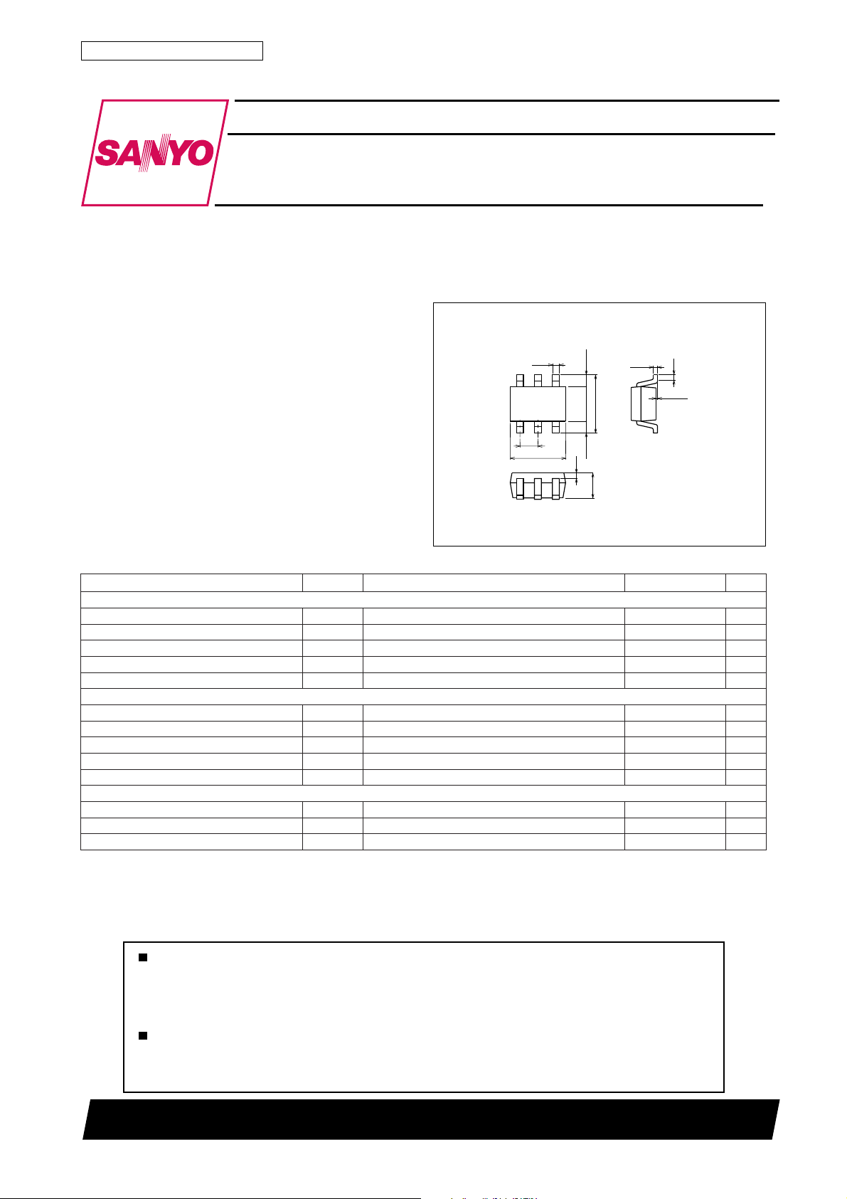
NPN Epitaxial Planar Silicon Composite Transistor
VCO OSC Circuit Applications
Ordering number:ENN6220
FH202
SANYO Electric Co.,Ltd. Semiconductor Company
TOKYO OFFICE Tokyo Bldg., 1-10, 1 Chome, Ueno, Taito-ku, TOKYO, 110-8534 JAPAN
Features
· Composite type with a buffer transistor (2SC5226)
and a oscillator transistors (TS4162) contained in the
currently provided MCP package as a VCO oscillator, improving the mounting efficiency greatly.
· The FH202 is formed with two chips, being equivalent to the 2SC5245 and TS4162, placed in one
package.
· Optimal for use in oscillator circuit for VHF to UHF
band.
Specifications
Absolute Maximum Ratings at Ta = 25˚C
retemaraPlobmySsnoitidnoCsgnitaRtinU
]6225CS2[1rT
egatloVesaB-ot-rotcelloCV
egatloVrettimE-ot-rotcelloCV
egatloVesaB-ot-rettimEV
tnerruCrotcelloCI
noitapissiDrotcelloCP
]2614ST[2rT
egatloVesaB-ot-rotcelloCV
egatloVrettimE-ot-rotcelloCV
egatloVesaB-ot-rettimEV
tnerruCrotcelloCI
noitapissiDrotcelloCP
]snoitacificepsnommoC[
noitapissiDlatoTP
erutarepmeTnoitcnuJjT 051
erutarepmeTegarotSgtsT 051+ot55–
OBC
OEC
OBE
C
C
OBC
OEC
OBE
C
C
T
Package Dimensions
unit:mm
2160
[FH202]
0.25
6
12
0.65
2.0
54
3
0.2
0.4250.425
1.25
0.9
2.1
0.15
0 to 0.1
0.2
1 : Collector1
2 : Emitter1
3 : Collector2
4 : Base2
5 : Emitter2
6 : Base1
SANYO : MCP6
02V
01V
2V
07Am
051Wm
02V
21V
2V
05Am
051Wm
002Wm
˚C
˚C
N0199TS (KOTO) TA-1708 No.6220–1/9
Page 2
Electrical Characteristics at Ta = 25˚C
retemaraPlobmySsnoitidnoC
]6225CS2[1rT
tnerruCffotuCrotcelloCI
tnerruCffotuCrettimEI
niaGtnerruCCD
tcudorPhtdiwdnaB-niaGf
ecnaticapaCtuptuO
niaGrefsnarTdrawroF
erugiFesioN
]2614ST[2rT
tnerruCffotuCrotcelloCI
tnerruCffotuCrettimEI
niaGtnerruCCD
tcudorPhtdiwdnaB-niaGf
ecnaticapaCtuptuO
niaGrefsnarTdrawroF
erugiFesioN
Marking : 202
Electrical Connection
E2
B2B1
V
OBC
OBE
h
EF
T
boC
BC
V
BE
V
EC
V
EC
V
BC
2
V
|e12S|
EC
FNVECI,V5=
V
OBC
OBE
BC
V
BE
hEF1VECI,V2=
hEF2VECI,V2=
V
T
boC
EC
V
BC
2
V
|e12S|
EC
FNVECI,V2=
FH202
nimpytxam
I,V01=
0=0.1Aµ
E
I,V1=
0=01Aµ
C
I,V5=
Am02=
C
I,V5=
Am02=
C
zHM1=f,V01=
I,V5=
C
C
I,V01=
0=0.1Aµ
E
I,V1=
0=01Aµ
C
Am3=
C
C
I,V2=
Am3=
C
zHG1=f,Am02=
zHG1=f,Am7=0.18.1Bd
Am05=
zHM1=f,V01=
I,V2=
C
C
zHM051=f,Am3=
zHM051=f,Am3=8.10.3Bd
09002
921Bd
08002
07
0.17.1zHG
3161Bd
sgnitaR
7zHG
57.02.1Fp
1.18.1Fp
tinU
TR1
C1 E1 C2
3
2
100
FE
7
5
3
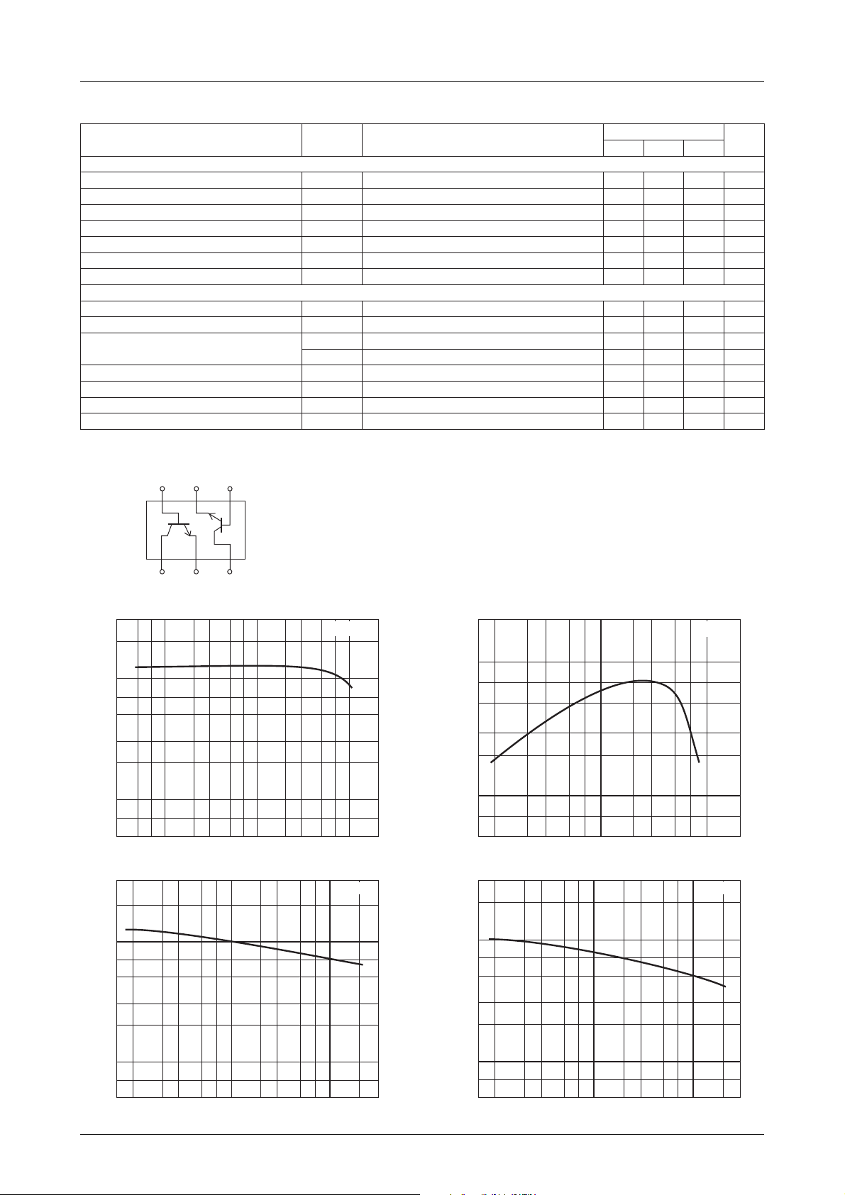
2
DC Current Gain, h
10
7
5
3
2
1.0
h
23 577
Cob -- V
TR2
FE
-- I
10
CB
C
23 57
[Tr1]
VCE=5V
100
IT00357
[Tr1]
f=1MHz
f
-- I
T
2
10
– GHz
7
T
5
3
2
1.0
Gain-Bandwidth Product, f
7
235
5
3
2
1.0
23 5 5772237
Collector Current, IC–mACollector Current, IC–mA
Cre -- V
C
10 100
CB
[Tr1]
VCE=5V
IT00358
[Tr1]
f=1MHz
1.0
7
5
3
2
Output Capacitance, Cob – pF
0.1
7
5
7
0.1
23 57
1.0
23 2 357
Collector-to-Base Voltage, VCB-- V
10
IT00359
1.0
7
5
3
2
0.1
7
Reverse Transfer Capacitance, Cre – pF
5
7
23 57
0.1
1.0
Collector-to-Base Voltage, VCB-- V
23 2357
10
IT00360
No.6220–2/9
Page 3
12
10
8
6
4
Noise Figure, NF – dB
2
0
57 57
1.0
Collector Current, IC–mA
220
200
180
– mW
160
150
C
140
120
100
80
60
40
Collector Dissipation, P
20
0
0 16014012010080604020
Ambient Temperature, Ta – °C
NF -- I
23357223
P
C
10 100
-- Ta
C
Total dissipation
1 unit
[Tr1]
VCE=5V
f=1GHz
IT00361
[Tr1]
IT00363
FH202
–dB
2
Forward Transfer Gain, S21e
14
12
10
8
6
4
2
0
357
2
S21e
-- I
=5V
CE
V
2V
23 57 7
1.0
Collector Current, IC–mA
10 100
C
2235
[Tr1]
f=1GHz
IT00362
No.6220–3/9
Page 4

FH202
S parameter [Tr1]
f=100MHz, 200MHz to 2000MHz(200MHz Step)
j50
j25
j100
j150
j10
0
--j10
2.0GHz
10 25
V
=2V
CE
I
=3mA
C
--j25
2.0GHz
2.0GHz
V
CE
I
C
50
=5V
=20mA
0.1GHz
--j50
100
V
CE
I
=7mA
C
0.1GHz
150
=5V
0.1GHz
j200
j250
250
--j250
--j200
--j150
--j100
IT00364 IT00365
f=100MHz, 200MHz to 2000MHz(200MHz Step) f=100MHz, 200MHz to 2000MHz(200MHz Step)
f=100MHz, 200MHz to 2000MHz(200MHz Step)
0.1GHz
°
90
°
±180
150
°
--150
°
0.1GHz
0.1GHz
°
120
V
--120
CE
I
C
V
I
C
°
=5V
=7mA
=2V
CE
=3mA
V
I
C
2.0GHz
=5V
CE
=20mA
2.0GHz
°
--90
2.0GHz
60
--60
°
°
30
20161284
0
°
--30
°
±180
150
°
--150
°
90
°
120
V
°
I
C
0.1GHz
0.1GHz
0.1GHz
2.0GHz
=5V
CE
=20mA
V
=5V
CE
I
=7mA
C
0.04 0.08 0.12 0.16 0.2
°
60
2.0GHz
2.0GHz
V
CE
I
=3mA
C
=2V
30
j25
°
j10
0
10 25
V
CE
I
=7mA
C
=5V
0
--j10
°
--120
°
°
--90
--60
°
--30
IT00366
°
--j25
j50
50
2.0GHz
2.0GHz
2.0GHz
--j50
V
I
C
100
V
I
C
CE
=3mA
=5V
CE
=20mA
=2V
150
j100
--j100
j150
250
--j150
IT00367
j200
j250
--j250
--j200
No.6220–4/9
Page 5

FH202
S Parameters (Common emitter) [Tr1]
VCE=5V, IC=7mA, ZO=50Ω
)zHM(qerFS|11|
001027.00.64–379.715.841030.05.86088.06.32–
002216.09.08–729.313.721740.01.75796.06.73–
004794.03.121–656.80.501660.03.15974.06.74–
006654.05.341–080.68.29970.09.25283.05.05–
008044.06.751–527.43.48490.04.55933.08.15–
0001634.05.761–468.30.77011.08.65323.04.35–
0021434.01.671–852.33.07621.09.75213.08.55–
0041334.06.671–748.25.46341.04.85403.03.85–
0061334.09.071–923.24.75061.09.85692.00.26–
0081434.00.561–252.22.45871.06.85392.00.56–
0002934.06.951–750.22.94791.01.85492.01.86–
∠ S
11
S|12|
VCE=5V, IC=20mA, ZO=50Ω
∠ S
12
S|21|
∠ S
21
S|22|
∠ S
22
)zHM(qerFS|11|
001184.08.87–597.929.231220.09.36707.02.83–
002024.02.911–800.912.211330.08.06074.01.15–
004193.06.151–614.014.59250.07.46692.03.55–
006683.04.661–480.76.68170.02.76632.01.65–
008183.09.571–704.51.08290.04.86312.06.65–
0001283.02.871104.41.47411.08.76802.09.75–
0021583.01.271107.35.86431.08.66402.07.06–
0041883.07.661712.36.36651.06.56202.05.36–
0061093.01.261938.28.85671.00.46991.09.76–
0081193.07.651435.23.45791.04.2679102.17–
0002493.01.251913.21.05912.06.06791.02.47–
∠ S
11
S|12|
∠ S
12
S|21|
∠ S
21
VCE=2V, IC=3mA, ZO=50Ω
)zHM(qerFS|11|
001858.04.23–314.92.751040.06.27549.05.61–
002287.07.06–781.85.831070.02.95338.03.92–
004356.01.101–558.58.311101.05.44736.02.34–
006885.05.621–733.44.89411.01.93515.00.05–
008755.07.341–444.37.78221.00.83454.08.35–
0001345.03.651–178.25.87031.06.83624.01.75–
0021635.08.661–644.25.07731.03.04704.03.06–
0041335.05.571–541.25.36641.05.24393.08.36–
0061725.00.771409.11.75551.00.54283.00.86–
0081525.03.071417.17.15861.03.7497300.27–
0002825.08.361465.19.54381.02.94873.08.57–
∠ S
11
S|12|
∠ S
12
S|21|
∠ S
21
S|22|
S|22|
∠ S
∠ S
22
22
No.6220–5/9
Page 6

FH202
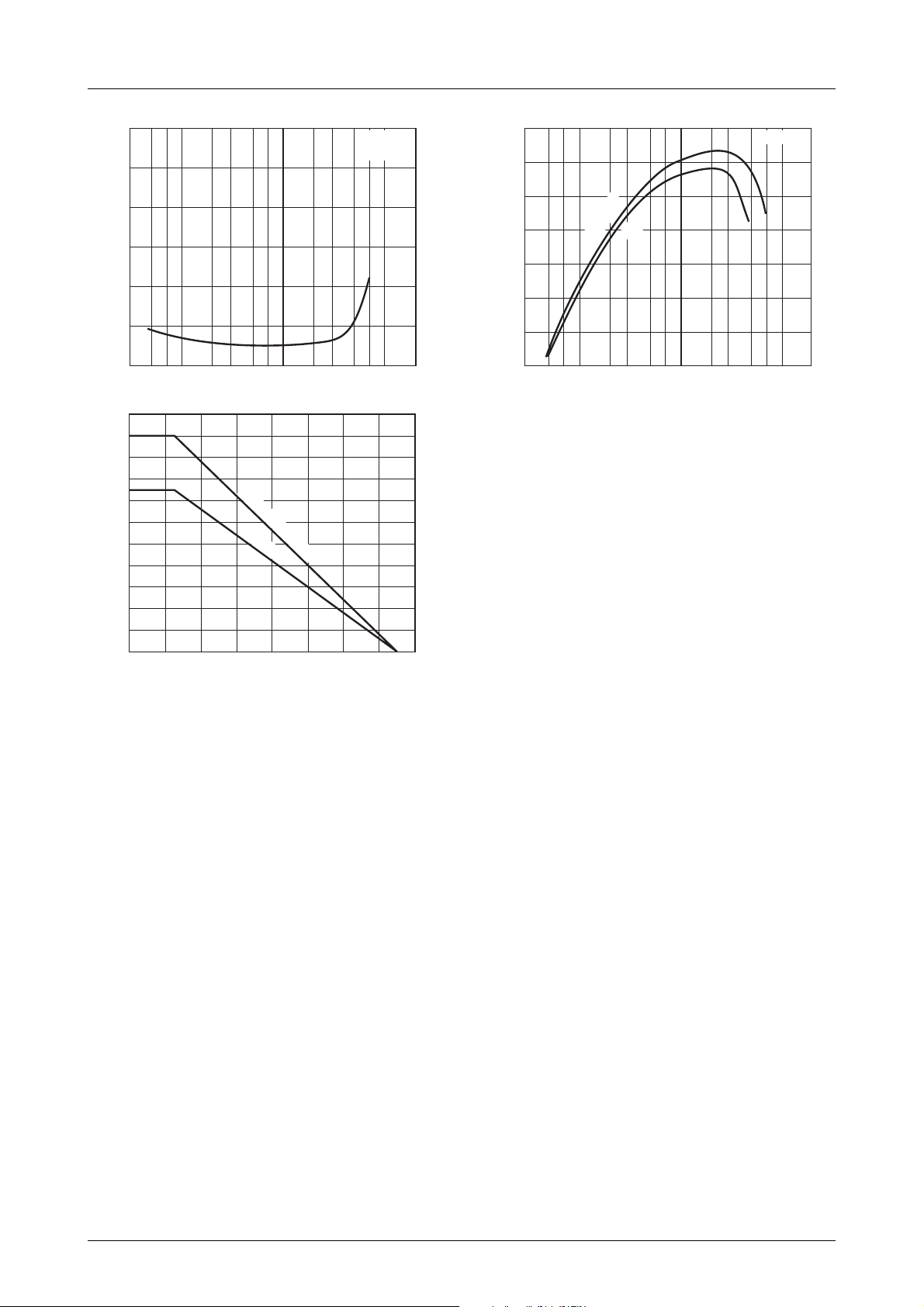
f
h
-- I
3
FE
C
[Tr2]
2
T
-- I
C
[Tr2]
2
FE
100
7
5
3
DC Current Gain, h
2
10
357
5
3
2
1.0
7
5
3
2
Output Capacitance, Cob – pF
0.1
7
12
10
8
6
23 57 7
1.0
Cob -- V
23 57
0.1
Collector-to-Base Voltage, VCB-- V
1.0
NF -- I
VCE=2V
23 5
10
CB
23 2357
C
10
– GHz
1V
IT00368 IT00369
[Tr2]
f=1MHz
7
T
5
3
2
1.0
7
Gain-Bandwidth Product, f
5
1.0
3
1.0
5
3
2
7
5
3
2
23 5 577237
Collector Current, IC–mACollector Current, IC–mA
Cre -- V
V
10
CB
CE
=2V
1V
Reverse Transfer Capacitance, Cre – pF
0.1
10
IT00370
[Tr2]
f=150MHz
7
32
28
–dB
24
2
20
16
23 57
0.1
Collector-to-Base Voltage, VCB-- V
1.0
S21e
CE
V
=2V
2
1V
23 2357
-- I
C
[Tr2]
f=1MHz
10
IT00371
[Tr2]
f=150MHz
4
Noise Figure, NF – dB
2
0
220
200
180
– mW
160
150
C
140
120
100
80
60
40
Collector Dissipation, P
20
0
0 16014012010080604020
V
CE
=2V
1V
23 5 577723
1.0 10 100
Collector Current, IC–mA
P
-- Ta
C
Total dissipation
1 unit
Ambient Temperature, Ta – °C
IT00372
[Tr2]
IT00374
12
8
4
Forward Transfer Gain, S21e
0
357
23 57 7
1.0
Collector Current, IC–mA
10 100
23 5
IT00373
No.6220–6/9
Page 7

S parameter [Tr2]
S11e
f=50MHz to 500MHz(50MHz Step)
j25
j10
j50
j100
j150
j200
j250
FH202
S21e
f=50MHz to 500MHz(50MHz Step)
°
120
V
CE
I
150
°
50MHz
C
=2V
=3mA
90
°
500MHz
60
°
°
30
10 25
0
--j10
500MHz
V
I
CE
=3mA
C
--j25
S12e
f=50MHz to 500MHz(50MHz Step)
°
120
°
150
°
±180
°
--150
°
--120
50
=2V
--j50
°
90
V
=2V
CE
I
=3mA
C
50MHz
0.04 0.08 0.12 0.16 0.2
°
--90
250150100
50MHz
--j100
°
60
°
--60
500
--j250
--j200
--j150
IT00375 IT00376
±180
°
--150
°
°
--120
--90
°
12 16 2084
--60
°
S22e
f=50MHz to 500MHz(50MHz Step)
j50
30
j25
°
j100
j10
500MHz
0
0
10 25
50
500MHz
250150100
50MHz
500
--j10
V
°
--30
--j25
IT00377 IT00378
--j50
I
C
CE
=3mA
=2V
--j100
--30
j150
j200
--j250
--j200
--j150
0
°
j250
S Parameters (Common emitter) [Tr2]
VCE=2V, IC=1mA, ZO=50Ω
)zHM(qerFS|11|
05569.06.52–84.37.361040.03.57589.01.7–
001849.03.94–03.32.941570.08.26159.03.31–
051229.05.96–69.26.631101.08.15709.00.81–
002309.00.68–56.23.621911.09.24958.07.12–
052588.04.99–33.23.711131.09.53918.06.42–
003378.04.011–70.21.011931.01.03197.09.62–
053668.04.911–98.18.301541.04.52877.07.82–
004458.04.721–37.18.79741.02.12357.08.03–
054648.09.331–85.19.29841.07.71247.07.23–
005748.09.831–44.15.88841.00.51637.04.43–
∠ S
11
S|12|
∠ S
12
S|21|
∠ S
21
S|22|
∠ S
22
No.6220–7/9
Page 8

FH202
VCE=2V, IC=3mA, ZO=50Ω
)zHM(qerFS|11|
05909.09.53–34.94.851830.00.17949.08.41–
001378.02.66–03.80.141760.00.65948.01.62–
051638.08.98–30.76.721480.09.44447.04.33–
002518.03.601–49.59.711590.05.73856.00.83–
052497.01.911–50.54.011001.04.23095.04.14–
003487.07.821–63.43.401401.07.82055.02.34–
053977.03.631–09.34.99701.00.62815.07.44–
004967.01.341–64.38.49801.09.32394.08.54–
054767.01.841–31.33.19801.04.22474.02.74–
005667.01.251–38.28.78801.07.12364.05.84–
∠ S
11
S|12|
VCE=2V, IC=10mA, ZO=50Ω
)zHM(qerFS|11|
05577.09.16–45.323.541330.04.16638.04.43–
001137.02.101–13.718.421840.05.64426.02.55–
051907.03.421–60.317.211650.06.93184.00.76–
002407.07.631–22.015.501060.01.73783.08.57–
052596.03.641–34.82.001460.05.63533.04.08–
003596.06.251–90.72.69660.08.63692.03.58–
053596.06.751–12.67.29070.02.73072.04.78–
004496.00.261–54.58.98270.05.83542.04.19–
054696.09.461–48.45.78570.09.93132.03.59–
005496.07.761–93.40.58870.05.14222.09.79–
∠ S
11
S|12|
∠ S
∠ S
12
12
S|21|
S|21|
∠ S
∠ S
21
21
S|22|
S|22|
∠ S
∠ S
22
22
VCE=2V, IC=30mA, ZO=50Ω
)zHM(qerFS|11|
05746.06.89–05.739.921420.04.25566.06.16–
001756.01.431–69.225.111230.08.44844.07.09–
051366.05.941–90.610.301730.08.44353.08.701–
002566.06.751–33.218.79140.03.74803.08.911–
052466.02.361–59.93.49640.05.94682.01.821–
003766.03.761–53.83.19150.02.25172.09.331–
053966.02.071–32.70.98550.00.45852.09.831–
004276.00.371–33.69.68060.09.55352.04.341–
054076.09.471–46.51.58660.02.75152.05.641–
005176.06.671–80.53.38170.03.85052.04.841–
∠ S
11
S|12|
∠ S
12
S|21|
∠ S
21
S|22|
∠ S
22
No.6220–8/9
Page 9

FH202
Specifications of any and all SANYO products described or contained herein stipulate the performance,
characteristics, and functions of the described products in the independent state, and are not guarantees
of the performance, characteristics, and functions of the described products as mounted in the customer's
products or equipment. To verify symptoms and states that cannot be evaluated in an independent device,
the customer should always evaluate and test devices mounted in the customer's products or equipment.
SANYO Electric Co., Ltd. strives to supply high-quality high-reliability products. However, any and all
semiconductor products fail with some probability. It is possible that these probabilistic failures could
give rise to accidents or events that could endanger human lives, that could give rise to smoke or fire,
or that could cause damage to other property. When designing equipment, adopt safety measures so
that these kinds of accidents or events cannot occur. Such measures include but are not limited to protective
circuits and error prevention circuits for safe design, redundant design, and structural design.
In the event that any or all SANYO products(including technical data,services) described or
contained herein are controlled under any of applicable local export control laws and regulations,
such products must not be exported without obtaining the export license from the authorities
concerned in accordance with the above law.
No part of this publication may be reproduced or transmitted in any form or by any means, electronic or
mechanical, including photocopying and recording, or any information storage or retrieval system,
or otherwise, without the prior written permission of SANYO Electric Co. , Ltd.
Any and all information described or contained herein are subject to change without notice due to
product/technology improvement, etc. When designing equipment, refer to the "Delivery Specification"
for the SANYO product that you intend to use.
Information (including circuit diagrams and circuit parameters) herein is for example only ; it is not
guaranteed for volume production. SANYO believes information herein is accurate and reliable, but
no guarantees are made or implied regarding its use or any infringements of intellectual property rights
or other rights of third parties.
This catalog provides information as of November, 1999. Specifications and information herein are subject
to change without notice.
PS No.6220–9/9
 Loading...