

Page 1
TOKYO OFFICE
Tokyo Bldg., 1-10, 1 Chome, Ueno, Taito-ku, TOKYO, 110-8534 JAPAN
Telephone: 81-(0)3-3837-6339, 6340, 6342, Facsimile: 81-(0)3-3837-6377
•
SANYO Electric Co.,Ltd. Semiconductor Company Homepage
URL; http://www.semic.sanyo.co.jp/index_e.htm
This catalog provides information as of February, 2004. Specifications and information herein are subject to change without notice.
Printed in Japan / February 2004 2k PC Plan
Ordering number : EP58B
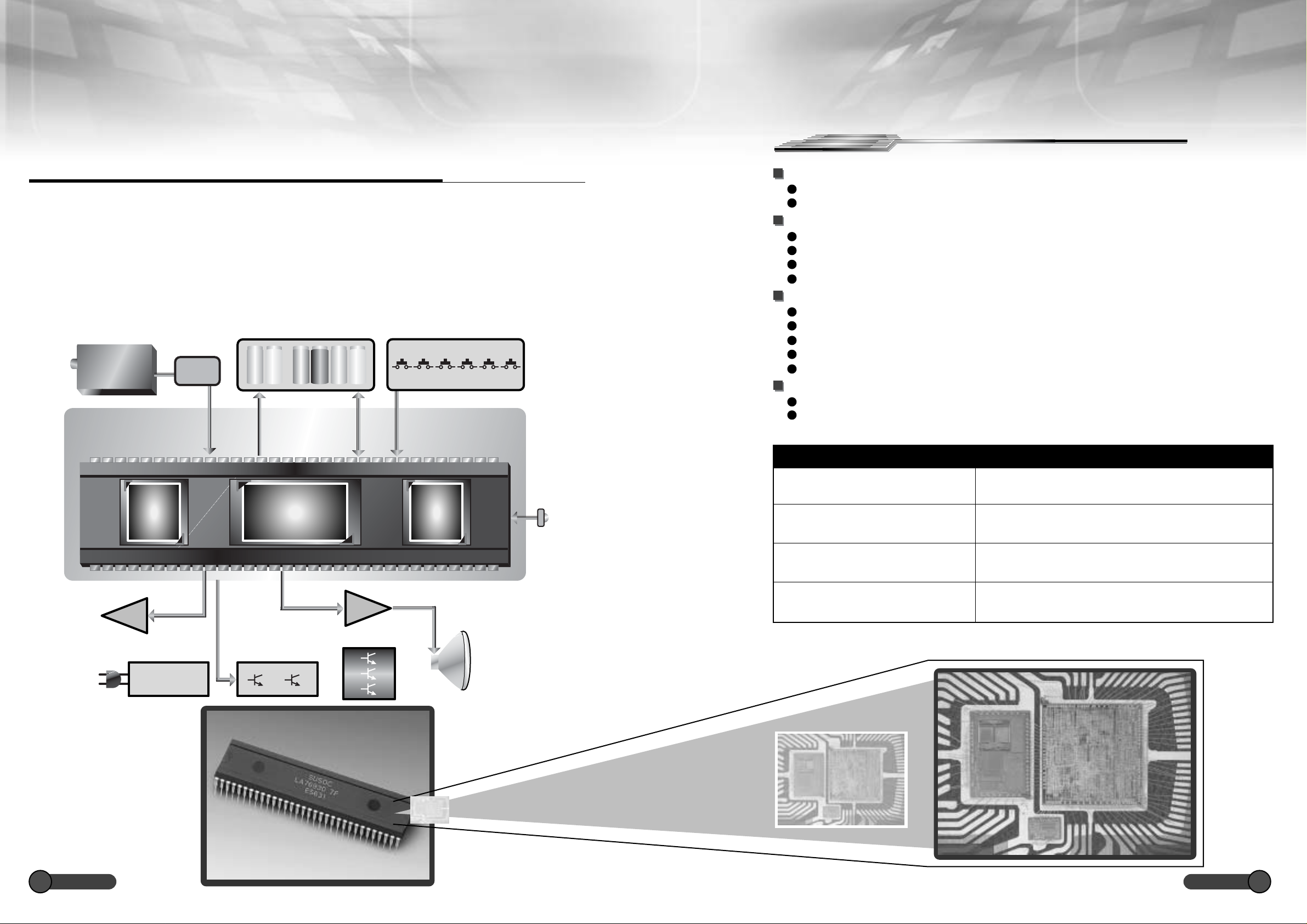
Digital TV, Analog TV,
Flat Panel Display, and VCR ICs
'04-2
Page 2
TV IC Lineup that Has Earned the
Top Market Share
CONTENTS
Digital TV Decoder System Chipset
Digital TV TS + Audio + Video Decoder IC with Built-in OSD Function
Digital TV 32-Bit RISC Microcontroller
Flat Panel Display Video Signal-Processing ICs
Scan Converter IC for Flat Panel Displays
Video Signal Processor
8-Bit Flash Microcontroll
2
Color TV I
Built-in CTV Microcontroller Signal-Processing System ICs
SUSOCTMLA76930 Series
Signal-Processing IC with Integrated Microcontroller
2
I
C Bus Control Lineup LA76810 Series
Vertical Output IC
LC863 Series
TV Control Microcontrollers (LC863 Series)
VHS Format VCR System Chip Set
Tuner IC
VIF/SIF Signal-Processing Circuit
PAL Hi-Fi Audio Signal Record and Playback Processing
Hi-Fi Signal Processing HiFi Processing with Built-in Audio Multiplex
Decoder for US Market Products
Hi-Fi Signal Processing HiFi Processing with Built-in Audio Multiplex
Decoder for Japanese Market Products
Video and Audio Signal-Processing IC
VCR SECAM Chrominance Signal-Processing IC
On-Screen Display Controller IC
VPS/PDC Slicer IC
VHF Band RF Module
PWM Capstan + Sensorless Drum + Loading Motor Drivers
Package Dimensions
: SUSOC
✽
These flash memory products are manufactured and sold by SANYO Electric Co., Ltd.
under license from Silicon Storage Technologies, Inc. (SST).
C Bus System Chip Set
.......................................................................................................................41.42
TM
is a trademark of SANYO Electric Co., Ltd.
.......................................................................................................10
er
..............................................................................................11.12
...................................................................................................24 to 34
s
.....................................................................................................35 to 36
.............................................................................................................60
.. ....................................................................................................61.62
............................................................................................64 to 66
....................................................................................6
....................................................................................15.16
.......................................................................19 to 23
...............................................................................43 to 49
..........................................................................................51
................................................................................52
........................................................................53 to 55
.................................................................................57 to 59
..................................................................3.4
........................................5
............................................7.8
...............................................................................9
.................................................................13.14
.........................................................17.18
.................................................................37 to 38
.................................................................39.40
.......................................................50
..................................................................56
....................................................63
New proposals from SANYO, the industry leader in
New proposals from SANYO, the industry leader in
TV IC sales worldwide.
TV IC sales worldwide.
SANYO has now developed the SUSOC(TM) series of
SANYO has now developed the SUSOC(TM) series of
on-chip microcontroller TV signal-processing ICs
on-chip microcontroller TV signal-processing ICs
that support all TV signal standards worldwide.
that support all TV signal standards worldwide.
SANYO was also one of the first companies to
SANYO was also one of the first companies to
respond to digital TV system needs with devices
respond to digital TV system needs with devices
based on SANYO's industry-leading bipolar technology.
based on SANYO's industry-leading bipolar technology.
SANYO provides powerful support as the curtain rises
SANYO provides powerful support as the curtain rises
on full-scale adoption of digital TV.
on full-scale adoption of digital TV.
For worldwide TV, for next generation TV,
For worldwide TV, for next generation TV,
SANYO ICs can help you open new markets worldwide.
SANYO ICs can help you open new markets worldwide.
Digital TV Decoder System Chip Set
SANYO 480i / 480p down decoder chipsets support both digital
satellite broadcast and digital terrestrial broadcast reception,
and are optimal for compact and popularly-priced TV sets.
Color TV I
SANYO's extensive lineup of color TV I
2
C Bus System Chip Set
2
C bus control system ICs
support design and manufacture of products appropriate for any
and all markets.
TM
SUSOC
Built-in CTV microcontroller TV signal-processing system ICs
Full lineup that covers all worldwide markets
Global pin-compatible series (Multiformat, PAL/NTSC, NTSC)
Any and all SANYO products described or contained herein do not have specifications that can handle
applications that require extremely high levels of reliability, such as life-support systems, aircraft's
control systems, or other applications whose failure can be reasonably expected to result in serious
physical and/or material damage. Consult with your SANYO representative nearest you before using
any SANYO products described or contained herein in such applications.
SANYO assumes no responsibility for equipment failures that result from using products at values that
exceed, even momentarily, rated values (such as maximum ratings, operating condition ranges, or other
parameters) listed in products specifications of any and all SANYO products described or contained
herein.
Specifications of any and all SANYO products described or contained herein stipulate the performance,
characteristics, and functions of the described products in the independent state, and are not guarantees
of the performance, characteristics, and functions of the described products as mounted in the customer's
products or equipment. To verify symptoms and states that cannot be evaluated in an independent device,
the customer should always evaluate and test devices mounted in the customer's products or equipment.
SANYO Electric Co., Ltd. strives to supply high-quality high-reliability products. However, any and all
semiconductor products fail with some probability. It is possible that these probabilistic failures could
give rise to accidents or events that could endanger human lives, that could give rise to smoke or fire,
or that could cause damage to other property. When designing equipment, adopt safety measures so
that these kinds of accidents or events cannot occur. Such measures include but are not limited to protective
circuits and error prevention circuits for safe design, redundant design, and structural design.
In the event that any or all SANYO products(including technical data,services) described or
contained herein are controlled under any of applicable local export control laws and regulations,
such products must not be exported without obtaining the export license from the authorities
concerned in accordance with the above law.
No part of this publication may be reproduced or transmitted in any form or by any means, electronic or
mechanical, including photocopying and recording, or any information storage or retrieval system,
or otherwise, without the prior written permission of SANYO Electric Co. , Ltd.
Any and all information described or contained herein are subject to change without notice due to
product/technology improvement, etc. When designing equipment, refer to the "Delivery Specification"
for the SANYO product that you intend to use.
Information (including circuit diagrams and circuit parameters) herein is for example only ; it is not
guaranteed for volume production. SANYO believes information herein is accurate and reliable, but
no guarantees are made or implied regarding its use or any infringements of intellectual property rights
or other rights of third parties.
LC863 Series
The LC863 Series devices are multifunction high-speed 8-bit
CMOS system microcontrollers that include OSD functionality.
This series provides simple and easy support for frequent
specification changes during production ramp up and
specification changes by target application by providing flash
ROM versions instead of the earlier erasable EPROM and
one-time programmable PROM versions.
In addition to the well-received large-capacity display RAM, the
LC864 Series provides a high-performance OSD function that
features increased CGROM capacity and provides a simple
graphics function.
VHS Format VCR System Chip Set
These products support high quality and high reliability in end
products by adopting adjustment-free technologies and
furthermore integrate even more peripheral components on the
same chip. This increased integration density promotes even
further reductions in the required circuit board mounting area.
Page 3
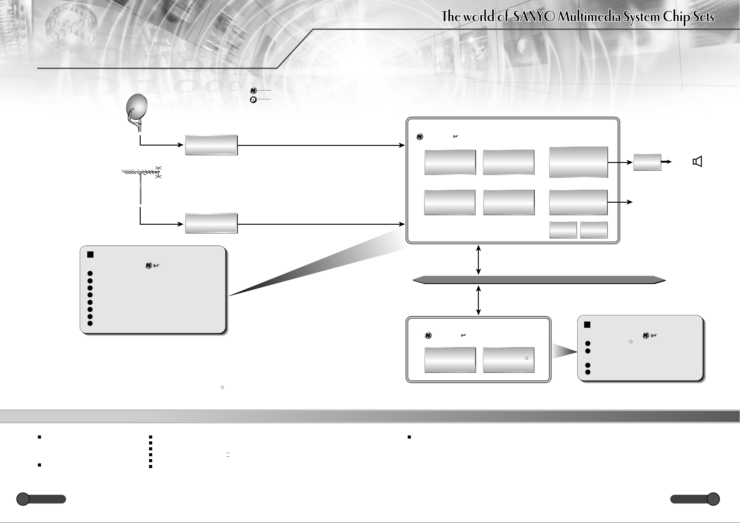
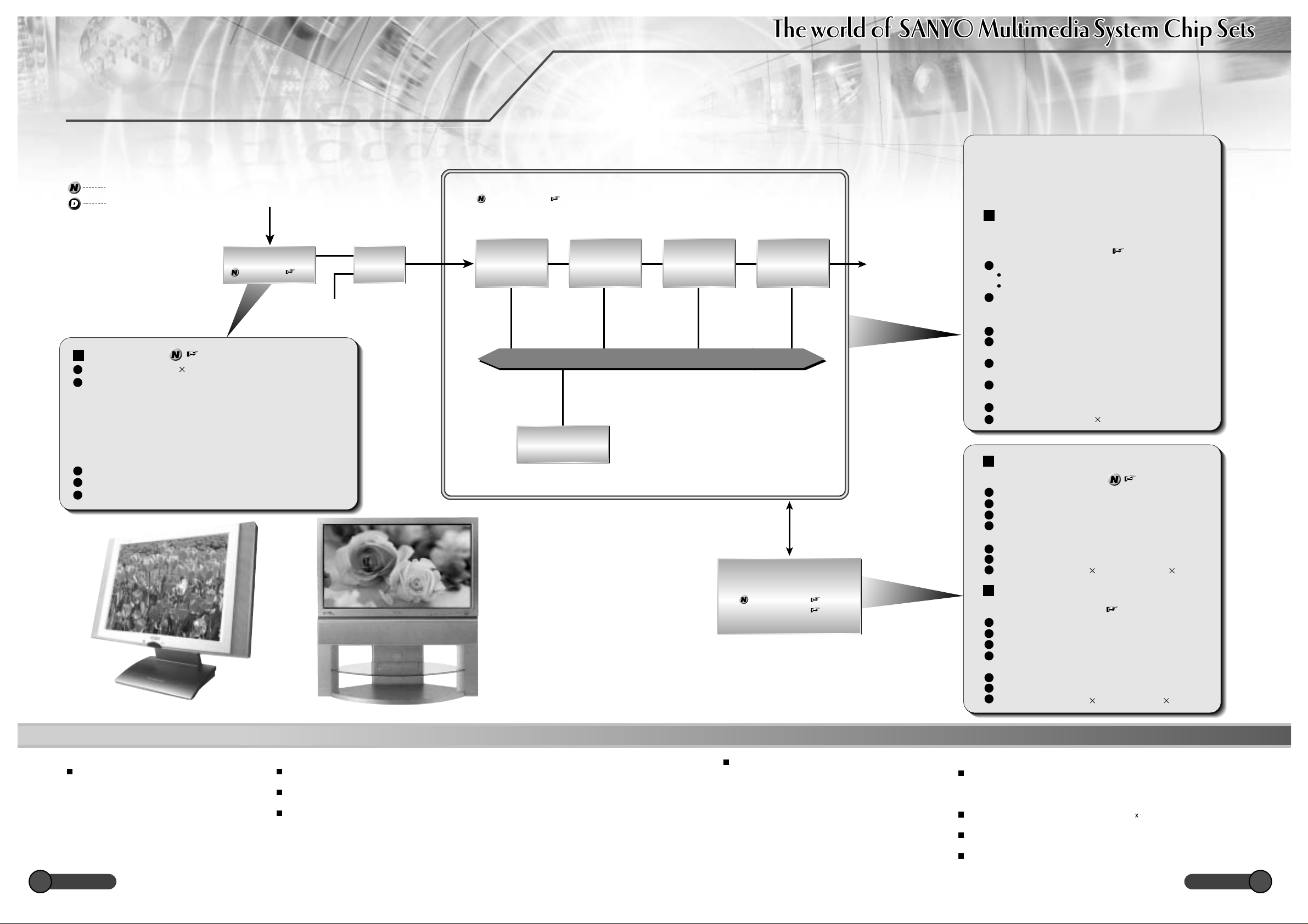
Digital TV Decoder
Digital TV Decoder
SANYO 480i / 480p down decoder chipsets support both digital satellite
SANYO 480i / 480p down decoder chipsets support both digital satellite
broadcast and digital terrestrial broadcast reception and
broadcast and digital terrestrial broadcast reception and
System Chip Set
System Chip Set
New product
Development
are optimal for compact and popularly-priced TV sets.
are optimal for compact and popularly-priced TV sets.
Satellite broadcast
antenna
BS
Terrestrial broadcast
antenna
Terrestrial
broadcast
signals
System-on-chip A/V decoder
LC74152B
MP@HL stream support (down decoding)
480i/480p video output
MPEG2 AAC/BC audio support
Built-in OSD function
NTSC encoder
Uses two external 64 Mbit SDRAMs
Supply voltage: 1.8 V/3.3 V
Package: PGBA352
P 5
Tuner
Tuner
Single-chip AV decoder
LC74152B
TS demultiplex
Descrambler
Microcontroller for digital TV
LC74186E
Peripheral
P 5
P 6
MPEG2
video decoder
OSD
controller
IBM PowerPC
Host bus
R
Audio decoder
Video scaler
D/AEncoder
D/A
Video
output
Audio
output
Digital TV microcontroller
LC74186E
IBM PowerPC
Includes UART, I
and PIO interfaces
Supply voltage: 3.3 V
Package: PQFP208
R
2
C, Smart Card, SIO,
P 6
: The following are trademarks of International Business Machines Corporation in the
✽
Unaited States,or other countries,or both. IBM,PowerPC
R
Extensive Lineup Provides Full System Support
RF amplifier transistors
Ultrahigh frequency transistors
2SC4869, 2SC5225, 2SC5501,
2SC5503, SBFP420M
TV tuner and VCR transistors
PicoGET Series
15GN01M, 55GN01M
SANYO TV . VCR SANYO TV . VCR
3 4
Power supply system peripheral transistors
High breakdown voltage MOSFET series
Ultralow on-resistance MOSFET series
Ultraminiature lightweight PicoMOSTM series
Ultralow saturation voltage MBIT-II transistor series
Low VF Schottky barrier diode series
PicoTR series
Muting circuit block
Muting transistor series
Page 4
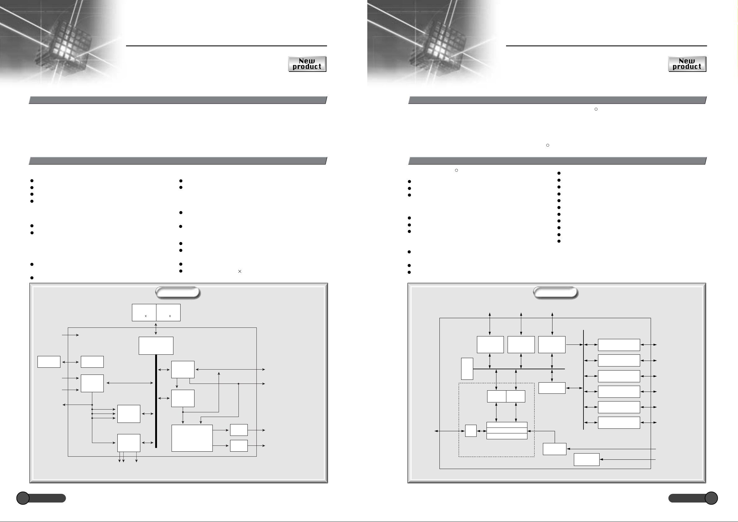
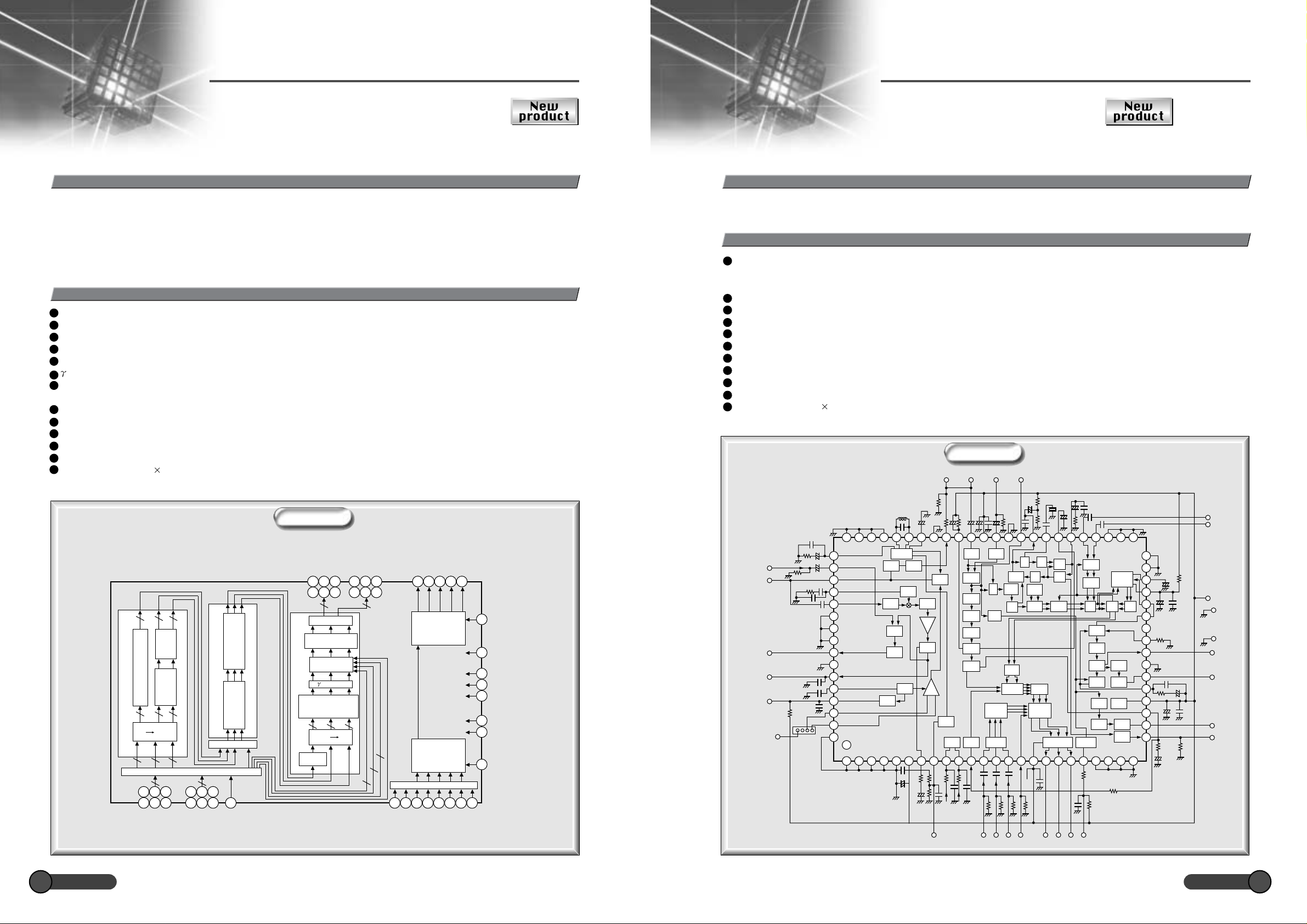
Digital TV TS + Audio + Video Decoder IC
with Built-in OSD Function
LC74152B
Overview
The LC74152B is a digital TV decoder IC that integrates MPEG2 video decoder, AAC audio decoder, transport stream decoder, data
broadcast OSD, video scaler, and NTSC encoder functions on the same chip.
The video decoder down decodes the HDTV stream to 480i/480p. The digital TV backend block can be implemented by combining
this IC with a system controller (CPU).
Functions
[TS Decoder Block]
Supports two TS channel inputs
8-bit parallel TS inputs
Either internal or external synchronization can be selected
Supports up to 55 indexes. The PID and channel number can
be set for each index.
[Video Decoder Block]
Down decodes the HD stream to 480i/480p
Supports two-channel HD down decoded playback,
two-channel HD down decoded plus 480p normal playback,
and three-channel 480p normal playback
[Audio Decoder Block]
MPEG AAC 5.1 channel decoding (with the output mixed
down to two channels)
MPEG BC decoding
[OSD Block]
Supports both 480i and 480p display
Supports both the 16 bits per pixel YUV 422 format and the
8 bits per pixel CLUT8 format
[Scaler Block]
Two scalers are provided, supporting two-screen structures or
video recording output
Supports satellite broadcast multi-view 3-screen display
[Encoder Block]
NTSC interlaced encoding
Can generate two video output systems
Supply voltage: 1.8 V (internal), 3.3 V (I/O)
Package: PBGA352 (35 35)
Digital TV 32-Bit RISC Microcontroller
LC74186E
Overview
The LC74186E is 32-bit microcontroller for digital TV that uses the IBM PowerPC as its CPU core and integrates on a single chip a
wide range of peripheral functions, including UART, I
2
C bus control, timer, synchronous serial port, parallel port, external SDRAM
control, and external bus control functions.
: The following are trademarks of International Business Machines Corporation in the
✽
Unaited States,or other countries,or both. IBM,PowerPC
R
Functions
[IBM PowerPC (PPC405D4)]
Operation at clock frequencies up to 216 MHz
16 KB instruction cache
16 KB data cache
[External SDRAM Control]
32-bit data bus
Support for two logical banks (two chip select signals)
Support for 4 MB to 256 MB per logical port
[External Bus Control]
Up to 8 ROM, EPROM, SRAM, flash, and slave peripheral
I/O banks (8 CS signals)
Support for both burst and non-burst transfer devices
26-bit address bus, 16-bit data bus
R
SCP (synchronous serial port): 1 channel
UART: 3 channels
2
I
C bus controller: 1 channel (I2C)
Smart Card interface: 1 channel
General-purpose timer (GPT)
General-purpose parallel port (GPIO)
Interrupt controller (UIC)
DMA controller (DMAC)
System clock generator PLL circuit
Supply voltage: 3.3 V
Package: PQFP208 (0.5 mm lead pitch, 28 mm square)
R
27MHz
Host CPU
TSIN1
TSIN2
TSOUT
(32bit 2M)
CPUIF
TS
VIDEO
AUDIO
(Main output: video recording output)
DAC I/F
Block Diagram Block Diagram
SDRAM
DIT(PCM&encoded stream)
SDRAM
(32bit 2M)
Arbiter
SCALER
OSD with
ISDB support
NTSC encoder
VDAC
VDAC
16-bit digital video interface
(SD input, main output)
8-bit digital video interface
(Recording output)
Three analog video channels
(Main outputs: Y.Pb.Pr/Y.C)
Three analog video channels
(Subsidiary output
: Y/C composite video)
Debugging
interface
ROM/SRAM control SDRAM control
ROM/SRAM
external
bus controller
Arbiter
Instruction
cache
JTAG
port
PPC405core
Memory management unit
Execution unit
Time
SDRAM
controller
Data
cache
16KB16KB
PLB
DMA control
DMA
controller
PLB/OPB
bridge
Interrupt
controller
OPB
Clock generator
PLL
Parallel port Parallel port
General-purpose timer
Smart Card interface
Asynchronous serial port Asynchronous serial port
Synchronous serial port
2
C bus controller I2C bus control
I
Timer I/O
Smart Card control
Synchronous 3-wire
serial port
Interrupt input
Clock inpu
SANYO TV . VCR SANYO TV . VCR
5 6
Page 5
Flat Panel Display Video
Flat Panel Display Video
Home AV Equipment Related DevicesHome AV Equipment Related Devices
Signal-Processing ICs
Signal-Processing ICs
Flat Panel Display System Chipsets
Optimal for Flat Panel Displays
New product
Development
LA7605M
Package: QIP80E (14 20) plastic package (flat package)
Functions: I
audio bandpass filter and trap, Y, C, and deflection
signal processing, CbCr internal (for DVD),
dynamic contrast support, one crystal oscillator
system (with built-in DDS circuit), external OSD
input, HS, VS, and BGP outputs, RGB analog
output
Applications: PAL/NTSC color TV
Supply voltage: 5 V single-voltage power supply
Power consumption: About 1 W
2
C bus controller, adjustment-free VIF/SIF,
P 10
LCD TV PDP TV
TV signal
(NTSC or PAL)
Decoder
LA7605M
Personal computer
(up to XGA resolution)
P 10
video signal
ADC
RGB
FPD video signal-processing IC
LC74986NWF
Input
processing
Timing control
P 9
Data bus
Scaling IP
Resolution
conversion
Picture quality
adjustments
These flash memory products are manufactured and
sold by SANYO Electric Co., Ltd. under license from
Silicon Storage Technologies, Inc. (SST).
SANYO has created video signal processing ICs that adopt high image quality scan
SANYO has created video signal processing ICs that adopt high image quality scan
converter technology and are optimal for flat panel displays.
converter technology and are optimal for flat panel displays.
Conversion of TV signals and
PC video signals to WXGA
resolution using resolution
conversion technology.
Video signal processing IC for
flat panel displays
Output
processing
LCD panel
(up to WXGA
resolution)
LC74986NWF
Support for multiple signal sources
NTSC/PAL and DTV (480i/480p) inputs
Up to XGA progressive scan input
Independent enlargement in the horizontal and
vertical directions. Reduction in the horizontal
direction is also provided.
Interlaced to progressive scan conversion
Built-in OSD function (On-chip 510-character,
8-color, font RAM 8 characters)
2
I
C bus interface (The OSD function can also be
controlled from a 3-wire bus)
Supply voltage: Dual-voltage supply - I/O: 3.3 V,
core: 2.5 V
Maximum operating frequency: 85 MHz
Package: SQFP144
(20 20)
P 9
8-bit flash microcontroller
P 11
P 12
Microcontroller
LC87F57C8A
LC87F5564A
P 11
P 12
LC87F57C8A
Flash ROM: 128 KB
RAM: 3,072 bytes
Minimum bus cycle time: 100 ns (10 MHz)
UART and synchronous serial port
( bus compatible)
12-channel 8-bit A/D converter
PWM: Two variable period 12-bit PWM circuits
Package: QIP64E
(14 14), SQFP64 (10 10)
8-bit flash microcontroller
LC87F5564A
Flash ROM: 64 KB
RAM: 1,024 bytes
Minimum bus cycle time: 100 ns (10 MHz)
UART and synchronous serial port
( bus compatible)
12-channel 8-bit A/D converter
PWM: Two variable period 12-bit PWM circuits
Package: QIP48E
(14 14), SQFP48 (7 7)
Extensive Lineup Provides Full System Support
AC/DC Converter Transistors
High breakdown voltage MOSFET series
2SK2624LS, 2SK2625LS, 2SK2628LS
SANYO TV . VCR SANYO TV . VCR
7 8
DC/DC Converter Transistors
Low saturation voltage transistors
CPH3115, CPH3109
Ultralow on-resistance MOSFETs
FSS140, FS132, FS134, CPH3314, CPH3414
Ultraminiature light weight PicoMOSTM series
2.5V drive: VDSS=30V system, N-channel and P-channel devices
2.5V drive: VDSS=50V system, N-channel and P-channel devices
4.0V drive: VDSS=50V system, N-channel and P-channel devices
Diodes
SBS004, SBS005, SBS006, SBE001, SBE002
Backlight Inverter Transistors
Low saturation voltage transistors
2SC5566, 2SC5706, 2SC5707,
CPH3216, CPH3205, CPH3212, CPH3223,
CPH3115, CPH3109, CPH3116, 2SA2039
Dual device single package products (PNP 2)
CPH5503, CPH5504 ,CPH5506, CPH5508
Dual device single package products (PNP + NPN)
CPH5506
MOSFETs
FW332, FW351, FW238, FW256
Page 6
Scan Converter IC for Flat Panel Displays
LC74986NWF
Overview Overview
The LC75986NWF is a video signal processing IC that performs resolution conversion, IP conversion, and image quality corrections
without requiring external memory. It can convert and display a wide variety of video signal formats for display on a flat panel
display. In particular, its image quality correction function adjusts the image quality to be optimal for display on a flat panel.
Its OSD function can display characters with a size optimal for the panel used. A video signal processing system for flat panel
displays can be implemented easily by combining this IC with video converter, A/D converter, and microcontroller ICs and an
LCD panel.
Functions
NTSC/PAL and DTV (480i/480p) inputs: YCbCr digital 8-bit signal inputs
Up to WXGA progressive scan input: RGB digital 8-bit signal input
Independent enlargement in the horizontal and vertical directions. Reduction in the horizontal direction is also provided.
Interlaced to progressive scan conversion
Image quality adjustment function (sharpness, color, tint, black stretch, brightness, contrast, white balance, black balance)
correction circuit (Look-up table system. Common characteristics for each 8-bit RGB color can be programmed.)
Single RGB 24-bit or 18-bit signal output or dual RGB 48-bit or 36-bit signal output (with built-in bit depth simulation and
conversion functions)
No external frame memory required (Input and output have the same frame period)
Built-in OSD function (On-chip 510-character 8-color, font RAM 8 characters)
2
I
C bus interface (The OSD function can also be controlled from a 3-wire bus)
Supply voltage: Dual-voltage supply - I/O: 3.3 V, core: 2.5 V
Maximum operating frequency: 85 MHz
Package: SQFP144 (20 20)
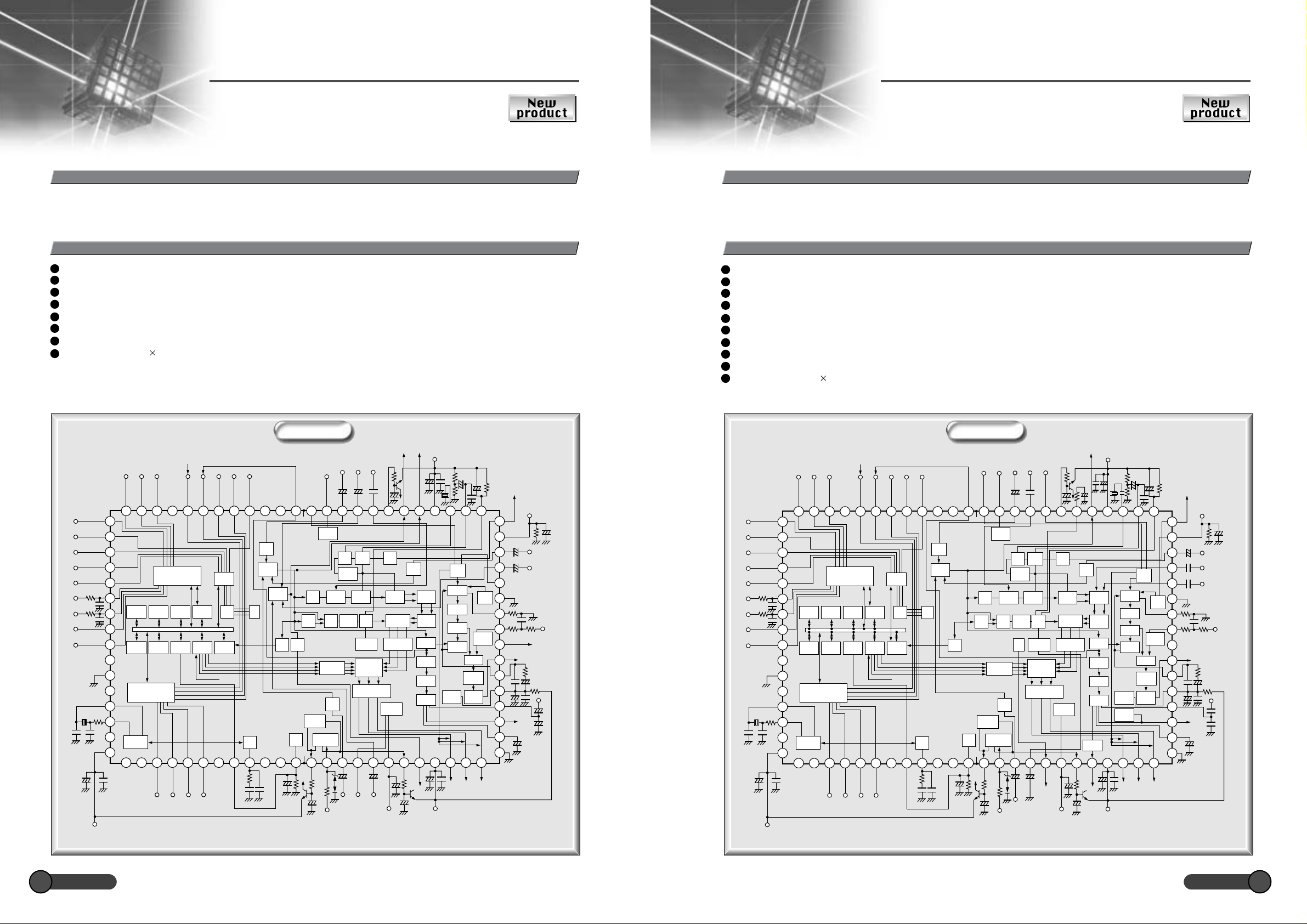
The LA7605M is a flat panel display color TV signal-processing I2C bus controller IC that supports all the broadcast standards used
worldwide.
Functions and Features
VIF/SIF bloc
· Adjustment-free VCO, 4-mode audio trap/audio bandpass filter, buzz canceller
· RF AGC/video level
Single crystal color system: PAL and NTSC
Black stretch, sharpness control with coring on/off control, built-in variable Y system filters (Y-DL and chrominance trap)
Chrominance bandpass filter, demodulation ratio/angle control, support for CbCr input
VS, HS, and BGP outputs, C-sync output, FSC output
Dynamic contrast control
VIF, SIF, video, and sync separator circuits with superlative weak field and nonstandard signal characteristics
Adjustment-free VIF/SIF, audio trap, and audio bandpass filters
Horizontal resonator-less adjustment-free system
Supply voltage: VCC: 5 V
Package: QIP80E (14 20)
Video Signal Processor
LA7605M
Block Diagram
INT-V IN
(S-C:IN)
EXT-V
SVO
IN
VIDEO
OUT
Y
SHARPNESS
Input Processing
Y
RGB Y Cb Cr
88
Data
24 24
VPA1[7:0]
Cb
COLOR TINT
Cb
8
135125117
128118110
VPA3[7:0]
VPA2[7:0]
Cr
Cr
Select
107
9989
100
9282
1
1
VPB2[7:0]*
VPB1[7:0]*
Horizontal and vertical
direction enlargement
Scaling Processing
Horizontal direction
reduction
Select
81
1
VPBEN
VPB3[7:0]*
Block Diagram
External
voltage
signals
BOUT[7:0]
GOUT[7:0]
ROUT[7:0]
716151
645444
OSD
Bit depth conversion
processing
MIX
correction
White balance
Output Processing
Contrast, Black balance
Brightness
RGB
Y Cb Cr RGB
Black
stretch
1
1
1
BOUT_2[7:0]*
GOUT_2[7:0]*
ROUT_2[7:0]*
107
9989
100
9282
2424
B
8
G
8
R
8
VSI
VS0
Output Timing
Input Timing
142 143141140
HSI
DEVI
HS0
Select
DEHI
DEV0
CLKI
DEH0
3438394041
2
VPBH
DCLK0
3117355
VPBCK
VPBV*
DCLKI
26
XTAL
25
AIC
19
AIDA
18
2
17
AICS*
SCL
14
SDA
13
CLKIEN
4
*1, *2: Register selectable
EXT AUDIO INT
S CARRIER OUT
AUDIO OUTPUT
PM OUT
RF AGC
IF IN
Ω
1k
F
µ
VCO
F
µ
TRAP
BPF
0.47
A2C
PLL
VIDEO
AMP
SPLL
SW
64
1000P
330
Ω
+
0.47µF
+
10
µ
F
600
Ω
µ
0.01
1k
Ω
1000P
10P
63 62 61 60 59 58 57 56 55 54 53 52 51 50 49 48 47 46 45 44 43 42 41
65
66
67
F
68
69
70
71
72
RF
AGC
VOL
CD
IF
AGC
73
74
(M)
75
µ
F
0.01
76
0.022µF
77
µ
F
0.01
30k
Ω
1
78
79
80
2.2
+
Ω
1k
+
VIDEO
DIT
BPF
LIM
AMP
FM
DET
VIF
AFT
BUS DCS CL AMP IRIVE/OUT-OFF C_SYNC
F
µ
Ω
1
680k
+
VIDEO
SW
TRAP
DELAY
LINE
PEAKING
CORING
BLACK
STRETCH
DC
REST
F
µ
100
+
F
µ
0.01
+
CLMPCLMP
SW
SYNC
SEP
OSD
FIX GAIN
ERIGHT
Ω
V/C
F
75
µ
1
GND
BPF
(ON/OFF)
AOC
COLOR
CLAMP
CONTRAST
ERIGHT
123456789101112131415161718192021222324
F(M)
0.01µF
100
Ω
Ω
100k
27k
Ω
+
µ
F
+
100k
F
µ
1
Ω
Ω
100
100
F
µ
0.1
100P
100P
AFT R IN
µ
0.01
G IN
F(M)
µ
0.01
Ω
Ω
75
75
B IN
Ω
µ
F
0.47
24k
+
VXD
APC1
F(M)
µ
0.01
Ω
75
FB IN R OUT G OUT B OUT
P(M)
µ
0.047
TINT
PAL
SW
DEMO
MATRIX
F
µ
10
Ω
10k
RGB
OSD
SW
DOD
+
Ω
24k
16P
APC2
VCO
CLAMP
+
F
µ
0.47
F
µ
1
1000P
Ω
0.1µF
1k
0.1µF
CLAMP
DC ADS
SW
HOR
VCO
1/256
HOR
C/D
AFC1
VER
SEP
VER
C/D
Ω
1k
Ω
30k
C_SYNC OUT
DELAY
+
PHASE
SHIFTER
HOR
OUT
HOR
VCC
VER
OUT
PSC
1k
Ω
CR_IN
CB_IN
40
39
IH
38
37
LPF
36
ALC
35
34
(METUL FILM)
33
32
Ω
F
100
+
µ
10
VCC 5V
F
+
F
µ
µ
10
REF
4.7k
Ω
0.01
GND
GND
BGP
31
F
µ
0.01
Ω
10k
HS
VS
FSC OUT
30
(M)
15000P
29
1µF
3.3k
Ω
28
+
F
µ
27
10
26
25
Ω
1k
+
F
µ
1
SANYO TV . VCR SANYO TV . VCR
9 10
Page 7
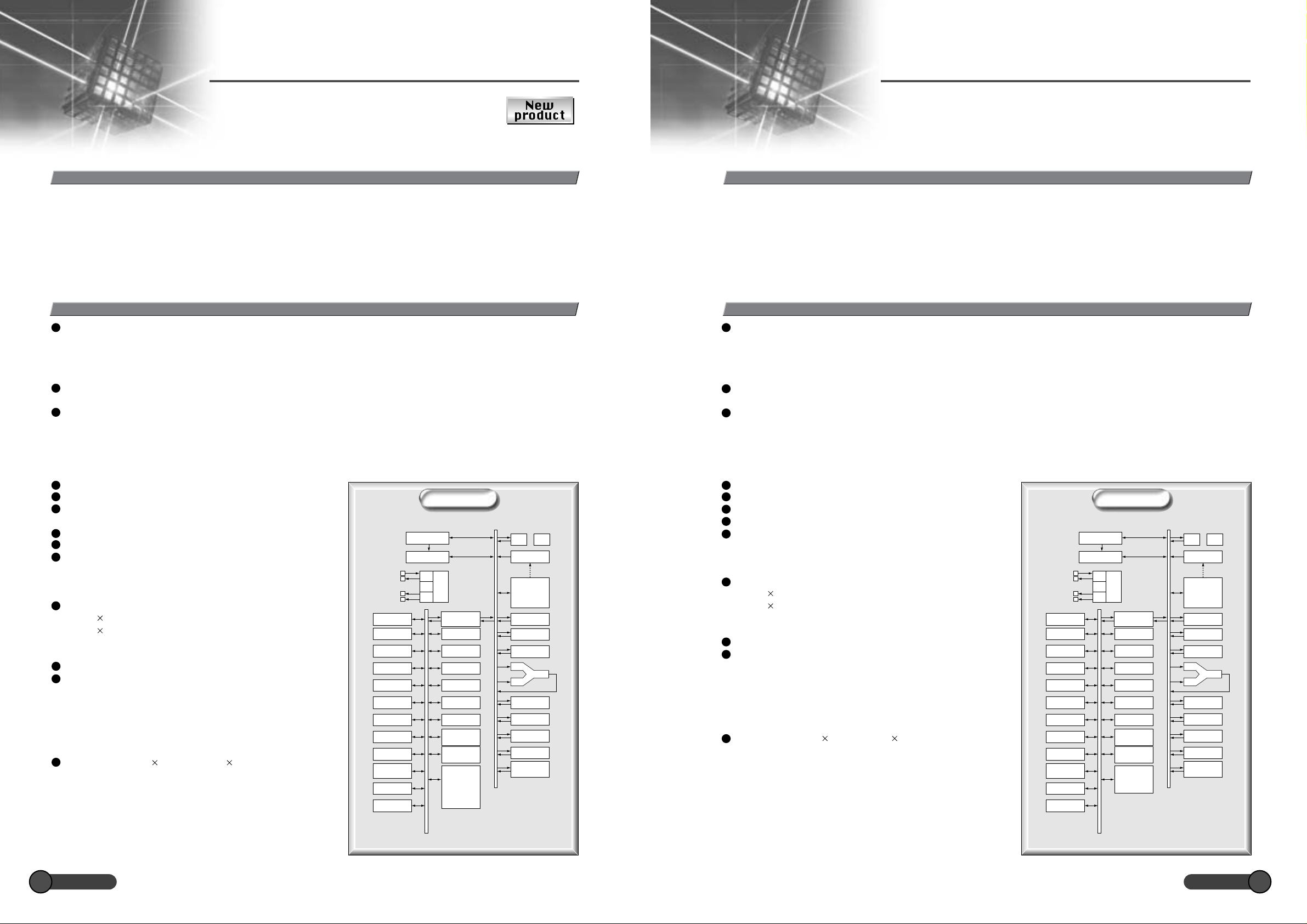
8-Bit Flash Microcontroller 8-Bit Flash Microcontroller
LC87F57C8A
Overview
The LC87F57C8A is an 8-bit microcontroller built around a CPU block that operates with a minimum bus cycle time of 100 ns and
that integrates 128 KB of flash ROM (that supports onboard programming), 4 KB of RAM, and an extensive set of peripheral
functions on a single chip. The peripheral functions include two multifunction 16-bit timer/counters (that can be used as separate
8-bit counters), four 8-bit timers with prescalers, a clock time base timer, two synchronous SIO channels that provide an automatic
transfer function, one asynchronous/synchronous SIO channel, two 12-bit PWM circuits, a 12-channel 8-bit A/D converter, a highspeed 8-bit parallel interface, a high-speed clock counter, a system clock divider function, and an interrupt function that supports 20
interrupts and 10 vector locations.
Functions
Timers
· One 16-bit timer/counter with capture register (can also be used as two 8-bit timers)
· One 16-bit timer/counter with PWM/toggle output function (can also be used as two 8-bit timers)
· Four 8-bit timers with 6-bit prescaler function
· Clock time base timer
High-speed clock counter
(Can count a clock signal up to 20 MHz when a 10 MHz main clock frequency is used.)
SIO
· Two 8-bit SIO channels with automatic transfer function
- Two 8-bit baud rate generators included
- Maximum clock: 4/3 tCYC
· One 8-bit asynchronous/synchronous SIO channel
- Asynchronous: 8 to 2048 tCYC, Synchronous: 2 to 512 tCYC
A/D converter: 12-channel 8-bit converter
PWM: two variable-period 12-bit PWM circuits
Parallel interface (switchable polarity, can perform read and write
operations in 1·tCYC)
Remote control receiver
(using the P73/INT3/T0IN shared function pin)
Watchdog timer (Uses an external RC circuit)
Interrupts
· 20 interrupt sources with 10 vector locations (Multiple interrupts
supported using three interrupt levels: low level (L), high level (H),
and maximum level (X))
High-speed multiply and divide instructions
· 16 bits 8 bits (Execution time: 5 tCYC)
· 24 bits 16 bits (Execution time: 12 tCYC)
· 16 bits ÷ 8 bits (Execution time: 8 tCYC)
· 24 bits ÷ 16 bits (Execution time: 12 tCYC)
System clock divider function
Standby functions
· Halt mode: instruction execution stopped, peripheral circuit
operation continues
· Hold mode: instruction execution stopped, peripheral circuit
operation stopped
· Crystal hold mode: instruction execution stopped, peripheral
circuit operation stopped except for the clock time base timer
Package: QIP64E (14 14), SQFP64 (10 10)
SIO 0
SIO 1
SIO 2
Timer 0
Timer 1
Timer 4
Timer 5
PWM0
PWM1
Clock time base
timer
Timer 6
Timer 7
Block Diagram
Interrupt control
Standby control
CF
RC
Clock
X'tal
INT0 to INT3
noise rejection
generator
Bus
interface
Port 0
Port 1
Port 3
Port 7
Port 8
ADC
Port 2
INT4,5
Parallel
interface
Port A
Port B
Port C
IR
PLA
Flash ROM
PC
ACC
Register B
Register C
ALU
PSW
RAR
RAM
Stack pointer
Watchdog
timer
LC87F5564A
Overview
The LC87F5564A is an 8-bit microcontroller built around a CPU block that operates with a minimum bus cycle time of 100 ns and
that integrates 64 KB of flash ROM (that supports onboard programming), 1 KB of RAM, and an extensive set of peripheral functions
on a single chip. multifunction 16-bit timer/counters (that can be used as separate 8-bit counters), four 8-bit timers with prescalers, a
clock time base timer, two synchronous SIO channels that provide an automatic transfer function, one asynchronous/synchronous SIO
channel, two 12-bit PWM circuits, a 12-channel 8-bit A/D converter, a high-speed 8-bit parallel interface, a high-speed clock counter,
a system clock divider function, and an interrupt function that supports 20 interrupts and 10 vector locations.
Functions
Timers
· One 16-bit timer/counter with capture register (can also be used as two 8-bit timers)
· One 16-bit timer/counter with PWM/toggle output function (can also be used as two 8-bit timers)
· Four 8-bit timers with 6-bit prescaler function
· Clock time base timer
High-speed clock counter
(Can count a clock signal up to 20 MHz when a 10 MHz main clock frequency is used.)
SIO
· Two 8-bit SIO channels with automatic transfer function
- Two 8-bit baud rate generators included
- Maximum clock: 4/3 tCYC
· One 8-bit asynchronous/synchronous SIO channel
- Asynchronous: 8 to 2048 tCYC, Synchronous: 2 to 512 tCYC
A/D converter: 12-channel 8-bit converter
PWM: two variable-period 12-bit PWM circuits
Remote control receiver (using the P73/INT3/T0IN shared function pin)
Watchdog timer (Uses an external RC circuit)
Interrupts
· 20 interrupt sources with 10 vector locations (Multiple interrupts
supported using three interrupt levels: low level (L), high level (H),
and maximum level (X))
High-speed multiply and divide instructions
· 16 bits 8 bits (Execution time: 5 tCYC)
· 24 bits 16 bits (Execution time: 12 tCYC)
· 16 bits ÷ 8 bits (Execution time: 8 tCYC)
· 24 bits ÷ 16 bits (Execution time: 12 tCYC)
System clock divider function
Standby functions
· Halt mode: instruction execution stopped, peripheral circuit operation
continues
· Hold mode: instruction execution stopped, peripheral circuit operation
stopped
· Crystal hold mode: instruction execution stopped, peripheral circuit
operation stopped except for the clock time base timer
Package: QIP48E (14 14), SQFP48 (7 7)
SIO 0
SIO 1
SIO 2
Timer 0
Timer 1
Timer 4
Timer 5
PWM0
PWM1
Clock time base
timer
Timer 6
Timer 7
Block Diagram
Interrupt control
Standby control
CF
RC
Clock
X'tal
noise rejection
generator
Bus
interface
Port 0
Port 1
Port 3
Port 7
Port 8
ADC
INT0 to INT3
Port 2
INT4,5
Port A
Port B
Port C
IR
PLA
Flash ROM
PC
ACC
Register B
Register C
ALU
PSW
RAR
RAM
Stack pointer
Watchdog
timer
This flash memory product is manufactured and sold by SANYO Electric Co., Ltd.
under license from Silicon Storage Technologies, Inc. (SST).
SANYO TV . VCR SANYO TV . VCR
11 12
This flash memory product is manufactured and sold by SANYO Electric Co., Ltd.
under license from Silicon Storage Technologies, Inc. (SST).
Page 8
Color TV Bus
Color TV Bus
System Chip Set
System Chip Set
Full lineup of system ICs that feature I2C
bus control
SANYO supports end product design and manufacture appropriate for all markets
SANYO supports end product design and manufacture appropriate for all markets
with a full product line of color TV I2C bus control system ICs.
with a full product line of color TV I2C bus control system ICs.
2
C Bus Control for TV
I
Signal-Processing ICs
P 35~38
TV Control Microcontrollers
LC8632 Series, LC8633 Series
LC8634 Series, LC8635 Series
LC838 Series
ROM: 12 to 64 KB
RAM: 512 to 640 bytes
Caption data slicer (LC8632/LC8634 Series)
Simple graphics function OSD
Multi-master I
ROM correction function
On-chip flash memory microcontrollers for evaluation
Packages:
Full Lineup of I
Output ICs
2
C bus system
DIP42S (600mil), QIP48E (14 14) (LC8632/33 Series)
DIP36S (400mil), MFP36SDJ (375mil) (LC8634/35 Series)
DIP42S (600mil), QIP48E (14 14) (LC838 Series)
2
C Bus Vertical
P 29~
LA7840/41/45N/46N/75/76
78040N/040/041/045
High reliability Low power consumption
Type
No.
LA7840
LA7841
LA7845N
LA7846N
LA7875N
LA7876N
LA78040N
LA78040
LA78041
LA78045
Package
SIP7H
SIP7H
SIP7H
SIP10H
SIP10HD
SIP10H
T0220-7H
T0220-7H
T0220-7H
T0220-7H
4.0°C/W
4.0°C/W
4.0°C/W
3.0°C/W
4.0°C/W
3.0°C/W
3.0°C/W 70V 1.8APP
3.0°C/W 70V 1.8APP
3.0°C/W 70V 2.2APP
3.0°C/W 92V 2.2APP
j-C
Output
voltage
(max)
70V
70V
85V
85V
110V
110V
Output
current
1.8APP
2.2APP
2.2APP
3.0APP
2.2APP
3.0APP
16 to 33V
16 to 38V
16 to 33V
16 to 33V
16 to 33V
16 to 33V
16 to 43V
On-Chip I2C Bus and E/W
Driver Circuits
LA7847, LA7848, LA7849
For large-screen and flat-screen CRT TVs
Type
No.
LA7847
LA7848
LA7849
Package
SIP10HD
SIP10HD
SIP10H
4.0°C/W 72V 2.2APP
4.0°C/W 92V 2.2APP
3.0°C/W 92V 2.2APP
j-C
Output
voltage
(max)
Output
current
V
CC
V
CC
16 to 34V
16 to 43V
16 to 43V
P
24
25
26
27
32
29
28
30
31
P
33
33
34
Full lineup that responds to
market needs
PAL multiformat I2C bus
control system ICs
LA76810 Series
LA76818A
(PAL/NTSC,YCbCr)
LA76828N
(PAL/NTSC,E/W,YCbCr)
LA76835A
(NTSC,E/W support)
LA76835NM
(NTSC,E/W,YCbCr)
LA76843N
(NTSC)
Adjustment-free VIF/SIF
Built-in trap and bandpass filter
Single crystal chrominance system
Built-in horizontal period (1H) delay line
Supply voltage: VCC = 5 V/9 V
Package: DIP54S
(600mil)
P 19
P 20
P 21
P 22
P 23
Signal-processing ICs with
built-in microcontroller
(CPU + VCD)
LA76919M
(NTSC)
LA76922M
(NTSC E/W YCbCr)
Built-in microcontroller TV signal-processing ICs
VCC = 5 V or 9 V
TV signal-processing functions
TV system control microcontroller
P 17
P 18
New product
Development
TV control
microcontrollers
P 35~38
LC8632 Series
LC8633 Series
LC8634 Series
LC8635 Series
LC8638 Series
LC863A Series
LC863B Series
Remote control
receiver block
Remote control
transmitter
microcontroller
LC587XXX Series
SUSOCTM ICs
(LA76930 Series)
P 15
(SANYO Ultimate Super One Chip LSI)
LA76930 (IF+VCD+CPU)
with YcbCr
LA76932 (IF+VCD+CPU)
with YcbCr & E/W
LA76936 (IF+VCD+Micon)
with YcbCr SECAM
LA76938 (IF+VCD+Micon)
with YcbCr & E/W
I2C bus control super single-chip system ICs
LA76810 Series
VIF
I2C bus
SIF
LA76950 (IF+VCD+Micon)
with YcbCr
LA76952 (IF+VCD+Micon)
with YcbCr & E/W
LA7695X (IF+VCD+Micon+3line Comb)
with YcbCr & E/W
P 19~
Video /Chroma
Hori. /Ver.
2
C Bus interface
I
RGB drive
RGB input
✽
These flash memory products are manufactured and
sold by SANYO Electric Co., Ltd. under license from
Silicon Storage Technologies, Inc. (SST).
: SUSOC
Tuner
U/V mixer/OSC.
LA79106V
U/V mixer/OSC.+PLL
LV4512V
Video
output
Horizontal
output
Vertical output
LA7840 Series
LA78040 Series
LA7847/48 Series
LA7849 Series
Audio
output
TM
is a trademark of SANYO Electric Co., Ltd.
P 41
P 42
P 24~34
CRT
Speaker
Extensive Lineup Provides Full System Support
Remote control transmitter microcontrollers
4-bit system-on-chip microcontrollers: LC587XXX series
Built-in LCD display circuit: 92 to 140 segments
ROM capacity: 2K 16 bits to 8K 16 bits
4-bit system-on-chip microcontrollers: LC573400 series
Built-in LCD display circuit: Up to 120 segments
ROM capacity: 4K or 6K 8 bits
SANYO TV . VCR SANYO TV . VCR
13 14
Flash microcontrollers
LC58F7416A lineup
4-bit system-on-chip microcontrollers: LC573100 series
Optimal for low-end remote controls that do not require LCD display
ROM capacity: 1K, 2K, or 4K 8 bits
VHF/UHF Tuner Transistors
High-frequency MOSFET series
High-frequency transistor series (fT=1 to 6 GHz)
PicoGET series
Video Transistors
Horizontal deflection output transistor series
Video output transistor series
Ultralow on-resistance MOSFETs
Power Supply System Transistors
High breakdown voltage MOSFET series
Ultralow on-resistance MOSFET series
Ultraminiature light weight PicoMOSTM series
Ultralow saturation voltage MBIT-II transistor series
Low VF Schottky barrier diode series
PicoTR series
Page 9
Built-in CTV Microcontroller
Built-in CTV Microcontroller
Signal-Processing System ICs
Signal-Processing System ICs
SUSOC
TM
TM
LA76930 SeriesSUSOC
LA76930 Series
FeaturesFeatures
Support for Worldwide Markets with All-in-One ICs
A newly-developed signal-processing IC, a microcontroller, and even a CCD.
There is no one other than SANYO who has included so much functionality in a single package.
Additionally, series deployment with pin-to-pin compatibility* means that users can handle TV
signal standards in different markets around the world by changing only certain specific
components.
These ICs, which SANYO has named SUSOC
powerful support for design and manufacturing for all markets.
: This allows different models to be used with essentially no changes to the pin layout.
✽
AV input
SAW filter
TUNER
TMTM
TM
(SANYO Ultimate Super One Chip), provide
Switch
SUSOCSUSOC
1 chip
1 chip
CCDCCD
++
(IF/V/C/D)
(IF/V/C/D)
CPUCPU
Remocon
RX
General features
Complete lineup that covers all markets worldwide
Global pin-to-pin series (multiformat, PAL/NTSC, NTSC)
VIF/SIF
Adjustment-free VIF/SIF
No VCO coil required
Built-in audio bandpass filter, four-system audio trap
Digital AFT system
V/C/D (Video/Chrominance/Deflection)
Blue stretching technology that creates high-quality images
DDS technology single crystal VCO system
DVD component signal inputs (YCbCr)
Built-in SECAM demodulator (LA76936, LA76938)
Special architecture and algorithms that create high-quality images
CPU
Up to 15 colors can be selected
Four colors per character
SUSOC ICs (LA76930Series)
LA76930 (IF+VCD+CPU)
with YcbCr
LA76932 (IF+VCD+CPU)
with YcbCr & E/W
LA76936 (IF+VCD+Micon)
with YcbCr SECAM
LA76950 (IF+VCD+Micon)
with YcbCr
LA76952 (IF+VCD+Micon)
with YcbCr & E/W
LA7695X (IF+VCD+Micon+3line Comb)
with YcbCr & E/W
Audio power
RGB drive
AC
Power
supply
SANYO TV . VCR SANYO TV . VCR
15 16
Pre drive
H out
V-out
CRT
LA76938 (IF+VCD+Micon)
with YcbCr & E/W
TM
: SUSOC
✽
is a trademark of SANYO Electric Co., Ltd.
CPUCPU
CCD
CCD
1 chip
1 chip
1 chip
1 chip
(IF/V/C/D)
(IF/V/C/D)
(IF/V/C/D)
(IF/V/C/D)
CCD
CCD
Page 10
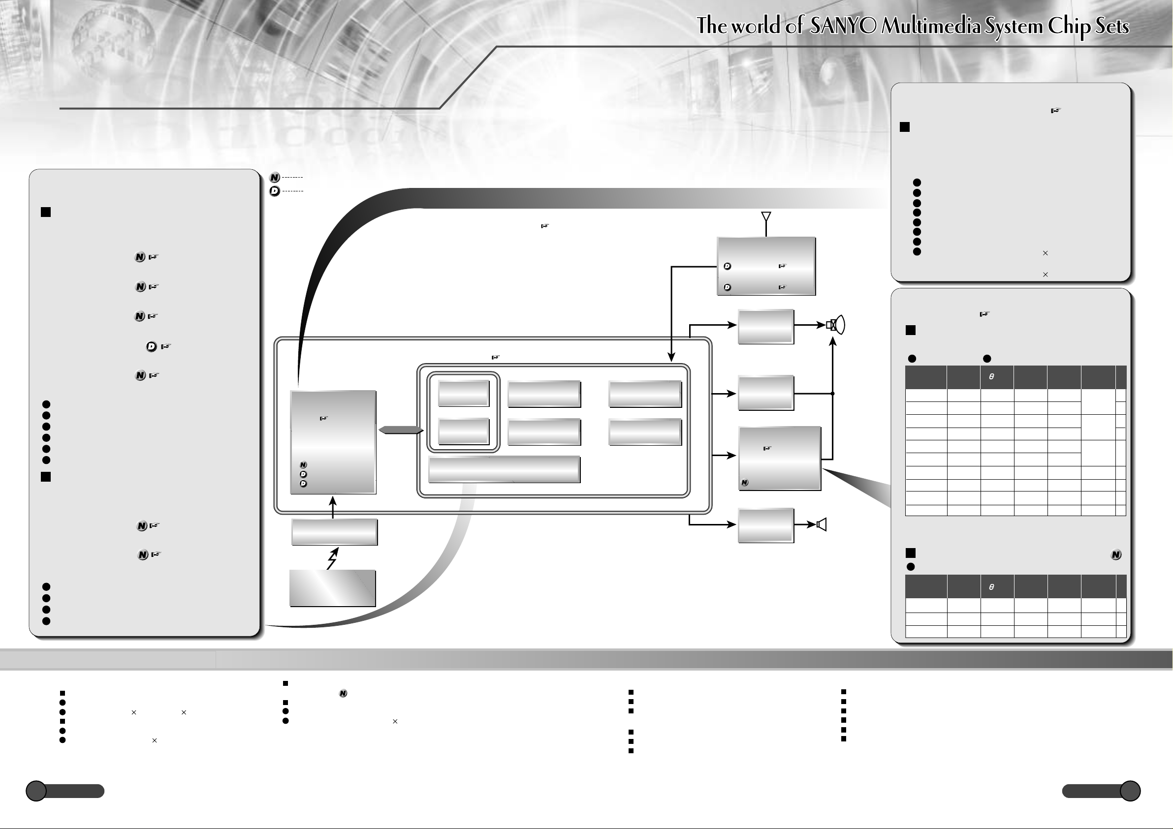
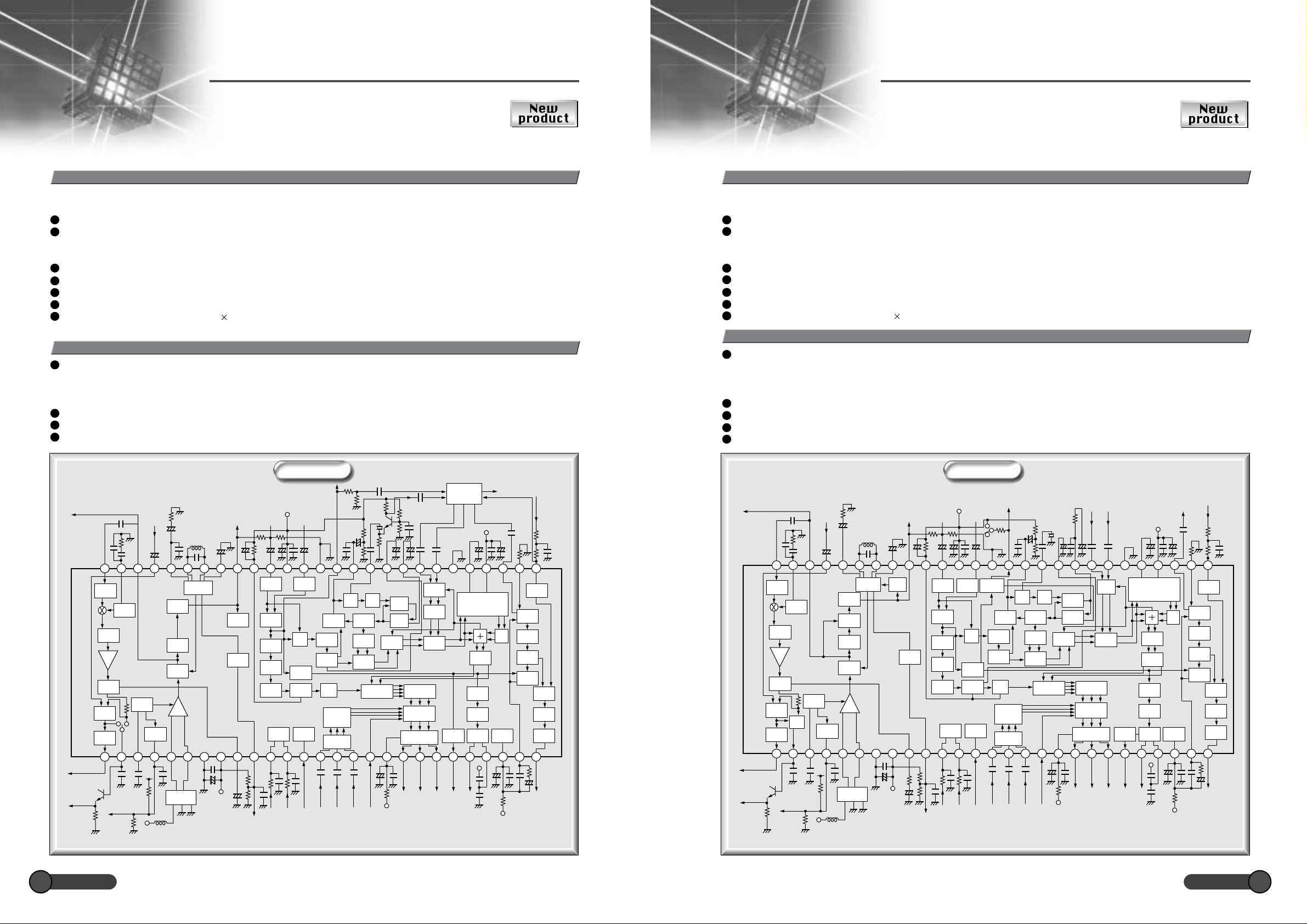
Signal-Processing IC with Integrated
Microcontroller
LA76919M
Overview Overview
The LA76919M and LA76922M series are I
TV set design, improved manufacturability, and lower total costs.
Functions and Features
Black stretch, sharpness control with coring on/off control, built-in variable Y system filters (Y-DL and chrominance trap)
Chrominance bandpass filter, demodulation angle control
Audio and video switching: three systems
Built-in microcontroller video, chrominance, and deflection signal processing
Adjustment- free horizontal resonator system
Simplified SG
Supply voltage: VCC = 11 V (built-in reference voltage for 5.7 V and 8.5 V regulators)
Package: QIP80E (14 20)
2
C bus controller ICs that support the NTSC format and aim for rationalization of color
The LA76919M and LA76922M series are I
TV set design, improved manufacturability, and lower total costs.
Functions and Features
Black stretch, sharpness control with coring on/off control, built-in variable Y system filters (Y-DL and chrominance trap)
Chrominance bandpass filter, demodulation angle control, CbCr input
E/W support
VM output
Audio and video switching: three systems
Built-in microcontroller video, chrominance, and deflection signal processing
Adjustment- free horizontal resonator system
Simplified SG
Supply voltage: VCC = 11 V (built-in reference voltage for 5.7 V and 8.5 V regulators)
Package: QIP80E (14 20)
Signal-Processing IC with Integrated
Microcontroller
LA76922M
2
C bus controller ICs that support the NTSC format and aim for rationalization of color
P17
P34
P35
P36
P37
P10/SDA0
P11/SCK0
P12/SDA1
P13/SCK1
+
Block Diagram Block Diagram
SAO
SVO
IR-IN
P03/INT3
P15/PWM2
P16/PWM3
P14/PWM1
P02/INT2
64 63 62 61 60 59 58 57 56 55 54 53 52 51 50 49 48 47 46 45 44 43 42 41
65
66
67
68
69
I/O
PORT 1
70
ADC
71
ROM RAM
I IC-BUS BUS BUS
72
BASE
73
TIMER
0
TIMER
CPU
CORE
OSD
74
75
76
I/O
PORT 0
77
78
79
CLOCK
CONTROL
80
23456789101112 13 14 15 16 17 18 19 20 21 22 23 24
1
P04/AN4
P05/AN5
P06/AN6
KEY-IN AFT
V
DD
P07/AN7
P01/INT1
I/O
PORT 3
DATA
SLICER
HS/VS
CSYNC
P00/INT0
PLL
P33
CLMP
VIDEO
SW
AUDIO
SW
LPF ATT
C INEXT-A
EXT-V
P-SW
+
+
+
REG
SW
VXO
APC 1 FSC
TINT
EPF
TRAP
CONTROL
REG-SW
5V/8V-REG
RST
+
11V
+
YC SW
V/Y
SW
OSD
CLMP
11V
ACC DEMO
DL
SHARP
DC REST
DRIVE/OUT-OFF
+
INT-V
SG
BS
OSD
SW
+
ABLREF
11V
RGB
MATRIX
CONTRAST
ERIGHT
ABL-ACL
INT-A
ABL
CLMP
+
+
AF
SW
COLOR
CLAMP
SYNC
SEP
VER
SEP
VER
C/D
VER
RAMP
ATT
OUT
VCC:5V
VCD
+
+
RGB
7.8V
+
+
X-RAY
HOR
VCO
X-RAY
1/256
HOR
C/D
FEP
AFC1
AFC2
PHASE
SHIFTER
HOR
HOR
VOC
OUT
R
OUTGOUTBOUT
40
39
38
37
36
35
34
33
32
31
30
29
28
27
26
25
FSC
+
+
HOR
GND
+
VER
OUT
VRAMP
+
X-RAY
V3
A3
H OUT
F
µ
8.47
+
+
FEP
KILLER OUT
HOR V
CC
+
+
P17
P34
P35
P36
P37
P10/SDA0
P11/SCK0
P12/SDA1
P13/SCK1
+
V
SVO
P15/PWM2
P16/PWM3
P14/PWM1
IR-IN
P03/INT3
P02/INT2
P00/INT0
P01/INT1
CSYNC
P33
X-RAY
IN
P-SW
64 63 62 61 60 59 58 57 56 55 54 53 52 51 50 49 48 47 46 45 44 43 42 41
EXT V
X-RAY
C IN
REF
+
+
+
11V
65
REG
RST
TRAP
REG-SW
11V
EPF
CONTROL
5V/8V-REG
+
SW
OSD
CLMP
11V
YC SW
V/Y
SW
+++
VXO
APC 1 FSC
TINT
ACC DEMO
DL
BS
SHARP
SG
DC RESTVM
OSD
SW
DRIVE/OUT-OFF
INT-V
YNR FIL
VM
OUT
RGB
MATRIX
CONTRAST
ERIGHT
ABL-ACL
+
ABL
CLMP
COLOR
CLAMP
E/W
AMP
E/W
OUT
66
67
68
69
I/O
PORT 1
I/O
PORT 3
CLMP
VIDEO
SW
70
ADC
71
ROM RAM
I IC-BUS BUS BUS
72
73
TIMER
0
BASE
TIMER
CPU
CORE
OSD
DATA
SLICER
LPF
74
75
76
I/O
PORT 0
HS/VS
77
78
79
CLOCK
CONTROL
80
DD
23456789101112 13 14 15 16 17 18 19 20 21 22 23 24
1
P04/AN4
P05/AN5
P06/AN6
KEY-IN AFT
P07/AN7
PLL
+
VCC:5V
+
AF/D1
SW
SYNC
SEP
VER
SEP
VER
C/D
VER
RAMP
+
VCD
HOR
VOC
VER
D/A
R
OUTGOUTBOUT
RGB
7.8V
HOR
VCO
1/256
HOR
C/D
AFC1
+
+
X-RAY
X-RAY
FEP
AFC2
PHASE
SHIFTER
HOR
OUT
40
39
38
37
36
35
34
33
32
31
30
29
28
27
26
25
FSC
+
HOR
GND
(METUL FILM)
H OUT
+
VER
OUT
VRAMP
+
X-RAY
V3
CR
CB
F
µ
8.47
+
FEP
+
HOR V
CC
SANYO TV . VCR SANYO TV . VCR
17 18
Page 11
I2 C Bus Control Lineup
LA76810 Series
LA76818A
Overview
The LA76810 series are I2C bus controller ICs that support the different TV broadcast formats used worldwide and aim for
rationalization of color TV set design, improved manufacturability, and lower total costs
Single crystal multiformat system that supports the different TV broadcast formats used worldwide
ICs optimal for each individual broadcast standard deployed as a pin-to-pin compatible lineup
· Multiformat system: LA76818A (YCbCr support), LA76828N (YCbCr and E/W support)
· NTSC system: LA76843N/LA76835A (YCbCr and E/W support), LA76835NM (YCbCr and E/W support)
Adjustment-free VIF/SIF, audio trap/audio bandpass filters
Adjustment- free horizontal resonator system
Simplified SG
Supply voltage: VCC = 5 V/9 V
Package: DIP54S (600mil), QIP80E (14 20) (LA76835NM only)
Functions and Features
VIF/SIF
· Adjustment-free VCO, 4-mode audio trap/audio bandpass filter, buzz canceller
· RF AGC/video level
· SIF system automatic discrimination (The LA7973 is used as the automatic discrimination IC.)
Single crystal color system: PAL, NTSC, SECAM (The LA7642N is used as the SECAM decoder.)
Black stretch, sharpness control with coring on/off control, built-in variable Y system filters (Y-DL and chrominance trap)
Chrominance bandpass filter, demodulation ratio and angle control
I2 C Bus Control Lineup
LA76810 Series
LA76828N
Overview
The LA76810 series are I
rationalization of color TV set design, improved manufacturability, and lower total costs
Single crystal multiformat system that supports the different TV broadcast formats used worldwide
ICs optimal for each individual broadcast standard deployed as a pin-to-pin compatible lineup
· Multiformat system: LA76818A (YCbCr support), LA76828N (YCbCr and E/W support)
· NTSC system: LA76843N/LA76835A (YCbCr and E/W support), LA76835NM (YCbCr and E/W support)
Adjustment-free VIF/SIF, audio trap/audio bandpass filters
Adjustment- free horizontal resonator system
Simplified SG
Supply voltage: VCC = 5 V/9 V
Package: DIP54S (600mil), QIP80E (14 20) (LA76835NM only)
Functions and Features
VIF/SIF
· Adjustment-free VCO, 4-mode audio trap/audio bandpass filter, buzz canceller
· RF AGC/video level
· SIF system automatic discrimination (The LA7973 is used as the automatic discrimination IC.)
Single crystal color system: PAL, NTSC, SECAM (The LA7642N is used as the SECAM decoder.)
Black stretch, sharpness control with coring on/off control, built-in variable Y system filters (Y-DL and chrominance trap)
Chrominance bandpass filter, demodulation ratio and angle control
E/W support
2
C bus controller ICs that support the different TV broadcast formats used worldwide and aim for
S CARRIER OUT
AUDIO OUTPUT
SAO
Block Diagram Block Diagram
SVO
V/C
EXT
AUDIO
IN
+
VCO
IF AGC
IF IN
RF AGC
V
CC
+
A2C
PLL
VIDEO
AMP
TRAP
VIDEO
DET
VIF
SAW
FILTER
54 53 52 51 50 49 48 47 46 45 44 43 42 41 40 39 38 37 36 35 34 33 32 31 30 29 28
BPF
SPLL
BPF
LIM
AMP
FM
DET
SW
DC
VOL
1 2 3 4 5 6 7 8 9 10 11 12 13 14 15 16 17 18 19 20 21 22 23 24 25 26 27
RF AGC
+
IF
VCC5V
+
VIDEO
OUT
IF
IDENT
IFT
+
+
VCC 5V
I IN-V IN
[S-C IN]
EXT-V IN
[Y-IN]
+
++
SW
LINE
BUS ABL
CLMP
SW
SYNC
SEP
BLACK
STRETOHDCREST
ABL
AFT
CLMP
VIDEO
TRAP
DELAY
PEAKING
CORING
V/C
GND
APC1 TINT
EPF
(ON/OFF)
ACC
OSD
CONTRAST
CLAMP
GINB
R
IN
+
VXO DDS
PAL
SW
DEMO
CONTRAST
ERIGHT
FB
IN
IN
CLAMP
+
RGB
VCC 9V
+
+
APC2
VCO
MATRIX
DRIVE/OUT-OFF
R
OUT
RGB
OSD
SW
G
OUTBOUT
ON
CLAMP
DC ADS.
SW
SECAM
DECODER
CCD/
HOR
GND
SYNC
SYNC
OUT
1H DELAY
COLOR
CLAMP
VER
SEP
VER
C/D
VER
RAMP
VER
OUT
SEOAM-KIL
SCP
CCD
VCC5V
REF
+
+
HOR
VCO
LPF
1/256
ALC
HOR
C/D
AFC1
HOR
VCC
+
HOR
VCC 9V
FBP
IN
FBP
AFC2
PHASE
SHIFTER
HOR
OUT
HOR
OUT
S CARRIER OUT
AUDIO OUTPUT
SAO
EXT-V IN
[Y-IN]
SW
SYNC
SEP
BLACK
ABL
FSC/SYNC
V/C
GND
FSC/
SYNC SW
BPF
(ON/OFF)
ACC
CONTRAST
R
IN
OUT
+
VXO DDS
APC1 TINT
PAL
SW
DEMO
OSD
BRIGHT
CLAMP
GINB
IN
CLAMP
CONTRAST
ERIGHT
+
FB
RGB
IN
VCC 9V
+
APC2
VCO
DRIVE/OUT-OFF
R
OUT
+
MATRIX
RGB
OSD
CB
CR
IN
IN
CLAMP
SW
SW
G
OUTBOUT
EW
E/W
OUT
CCD/
HOR
GND
1H DELAY
DC ADS.
COLOR
CLAMP
VER
SEP
VER
C/D
VER
RAMP
VER
OUT
VCC5V
+
CCD
+
LPF
ALC
HOR
VCC
+
HOR
VCC 9V
4M
OUT
REF
1/256
AFC1
HOR
VCO
HOR
C/D
+
V/C
EXT
AUDIO
IN
+
VCO
IF AGC
V
IF IN
+
RF AGC
CC
VIDEO
AMP
S.TRAP
SW
TRAP
VIDEO
DET
VIF
SAW
FILTER
A2C
PLL
54 53 52 51 50 49 48 47 46 45 44 43 42 41 40 39 38 37 36 35 34 33 32 31 30 29 28
BPF
SPLL
BPF
LIM
AMP
FM
DET
SW
SW
DC
VOL
1 2 3 4 5 6 7 8 9 10 11 12 13 14 15 16 17 18 19 20 21 22 23 24 25 26 27
RF AGC
OVER
MOD.
+
IF
VCC5V
+
VIDEO
OUT
AFT
+
+
VCC 5V
I IN-V IN
[S-C IN]
+
++
CLMP
CLMP
VIDEO
SW
TRAP
DELAY
LINE
PEAKING
STRETOHDCREST
CORING
BUS ABL
AFT
FBP
IN
FBP
AFC2
PHASE
SHIFTER
HOR
OUT
HOR
OUT
SANYO TV . VCR SANYO TV . VCR
19 20
Page 12

I2 C Bus Control Lineup
LA76810 Series
LA76835A
Overview
The LA76810 series are I2C bus controller ICs that support the different TV broadcast formats used worldwide and aim for
rationalization of color TV set design, improved manufacturability, and lower total costs.
Single crystal multiformat system that supports the different TV broadcast formats used worldwide.
ICs optimal for each individual broadcast standard deployed as a pin-to-pin compatible lineup.
· Multiformat system: LA76818A (YCbCr support), LA76828N (YCbCr and E/W support)
· NTSC system: LA76843N/LA76835A (YCbCr and E/W support), LA76835NM (YCbCr and E/W support)
Adjustment-free VIF/SIF, audio trap/audio bandpass filters
Adjustment-free horizontal resonator system
Simplified SG
Supply voltage: VCC = 5 V/9 V
Package: DIP54S (600mil), QIP80E (14 20) (LA76835NM only)
Functions and Features
VIF/SIF
· Adjustment-free VCO, buzz canceller
· RF AGC/video level/FM level control
Black stretch, sharpness control with coring on/off control, built-in variable Y system filters (Y-DL and chrominance trap)
Chrominance bandpass filter, demodulation angle control
E/W support
I2 C Bus Control Lineup
LA76810 Series
LA76835NM
Overview
The LA76810 series are I
rationalization of color TV set design, improved manufacturability, and lower total costs.
Single crystal multiformat system that supports the different TV broadcast formats used worldwide.
ICs optimal for each individual broadcast standard deployed as a pin-to-pin compatible lineup.
· Multiformat system: LA76918A (YCbCr support), LA76828N (YCbCr and E/W support)
· NTSC system: LA76843N/LA76835A (YCbCr and E/W support), LA76835NM (YCbCr and E/W support)
Adjustment-free VIF/SIF, audio trap/audio bandpass filters
Adjustment-free horizontal resonator system
Simplified SG
Supply voltage: VCC = 5 V/9 V
Package: DIP54S (600mil), QIP80E (14 20) (LA76835NM only)
Functions and Features
VIF/SIF
· Adjustment-free VCO, buzz canceller
· RF AGC/video level/FM level control
Black stretch, sharpness control with coring on/off control, built-in variable Y system filters (Y-DL and chrominance trap)
Chrominance bandpass filter, demodulation ratio and angle control, blue stretch
E/W support
2
C bus controller ICs that support the different TV broadcast formats used worldwide and aim for
AUDIO OUTPUT
FM OUT
RF AGC
IF IN
Block Diagram Block Diagram
F
µ
1
+
680K
CLMP
VIDEO
SW
TRAP
DELAY
LINE
PEAKING
CORING
BUS ABL
100
F
µ
0.1
EXT-V
IN
Y-IN
F
µ
F
µ
47
0.01
F
µ
1
+
+
CLMP
BPF
C SW
(BYPASS)
SYNC
SEP
BLACK
STRETOH
FIX GAIN
ERIGHT
F
IN
100P
µ
0.01
F
µ
0.01
100
100P
DC
REST
OSD
CLAMP
(M)
75
APC1
F
µ
0.01
(M)
+
ACC
F
µ
0.0
75
BINGINRINIB
16P
F
µ
1
VXO
KIL
CONTRAST
BRIGHT
F
µ
10
(M)
75
IN
V
CC
+
10k
X-RAYCWOUTSVO
1
µ
F
+
24K
0.47µF
F
+
µ
(M)
0.047
CW
DEMO CLAMP
COLOR TINT
DRIVE/OUT-OFF
F
µ
0.01
R
OUT
24K
H-OUT
CONTROL
RGB
MATRIX
OSD
SW
G
OUT
X-RAY
AUTO
FLESH
B
OUT
10k
1H-DL/
HOR
GND
E / W
OUT
EW
OUT
VER
OUT
VER
SEP
VER
C/D
VER
RAMP
(M)
CRC_ IN
F
µ
0.01
CLMP
CB.CR
SW
(M)
CB
F
F
µ
µ
REF
1
1
++
HOR
VCO
1/256
HOR
C/D
AFC1
HOR
VCC
H
V
CC
F
F
+
µ
µ
10
0.01
(M)
F
F
µ
µ
0.33
0.015
F
µ
0.33
+
EXT
S
AUDIO
OARRIER
IN
OUT
IF AGC
+
RF AGC
F
µ
(M)
0.022
F
µ
10
600
VIDEO
VIDEO
F
µ
0.01
1
+
AMP
TRAP
SW
SND
TRAP
DET
VIF
SAW
FILTER
VCO
330
F
µ
0.47
1000P
3K
F
µ
10P
0.01
54 53 52 51 50 49 48 47 46 45 44 43 42 41 40 39 38 37 36 35 34 33 32 31 30 29 28
BPF
SPLL
BPF
LIM
AMP
FM
DET
SW
DC
VOL
1 2 3 4 5 6 7 8 9 10 11 12 13 14 15 16 17 18 19 20 21 22 23 24 25 26 27
F
µ
0.01
30K
A2C
PLL
0.01µF
100µF
VIDEO
OUT
510
510
+
F
µ
F
µ
0.47
+
2.2
AFT
+
12K
+
µ
F
1
100K 100K
AFT FB
FBP IN
(METUL FILM )
4.7K
FBP
H OUT
AFC2
PHASE
SHIFTER
HOR
OUT
150
Ω
3.0K
F
µ
1
VCC 5V
GND
VCC 9V
GND
EXT AUDIO INT
S OARRIER OUT
AUDIO OUTPUT
FM OUT
RF AGC
IF IN
10P
30k
1
330
660
1000P
100
µ
0.022µF(M)
SVO
EXT-V IN
INT-V IN
DET
µ
H
15
F
µ
2.2
680k
510
AFT
100
100
100P
100P
[S-C : IN]
F
F
µ
µ
F
µ
0.01
0.01
+
1
DC
OSD
FIX GAIN
ERIGHT
F(M)
µ
0.01
757575
G IN
75
NC
CLMPCLMP
SW
IST AMP
BPF
2ND AMP
BPF
DEMO
COLOR
CLAMP
CONTRAST
BRIGHT
F(M)
F(M)
µ
µ
0.01
0.01
B IN FB IN
F
++
µ
1
VIDEO
SW
TRAP
DELAY
LINE
PEAKING
CORING
BLACK
STRETOH
REST
ACC
KILLER
CLMP
DELAY
CB.CR
SW
COLOR
HS/VS
10k
V/C/D
GND
MATRIX
20kHS20k
VS
RGB
OSD
SW
+
VIDEO OUT
510
39
+
V
CC
F
µ
0.47
EPF
SW
DC
VOL
A2C
PLL
VIDEO
AMP
SPLL
IF AGC
+
DET
EPF
LIM
ANP
FM
NC
VIDEO
VIF
64 63 62 61 60 59 58 57 56 55 54 53 52 51 50 49 48 47 46 45 44 43
GND
65
+
0.47µF
66
+
µ
F
10
67
µ
F
0.01
3k
68
69
70
NC
71
+
µ
F
10
72
NC
73
F
+
74
µ
F
0.01
75
0.01µF(M)
76
77
RF AGC
78
79
IF GND
80
GND GND
1
2 3 4 5 6 7 8 9 10 11 12 13 14 15 16 17 18 19 20 21 22 23 24
0.01µF
+
µ
F
100
BUS ABL OL AMP
100K
12K
F
+
µ
F
µ
0.1
1
100K
AFT ABL R IN
+
TINT
AUTO
FLESH
F
µ
10
VM IN
VCO
DRIVE/OUT-OFF
0.47
µ
16P
F
+
µ
F
µ
1
0.0471
CW
KIL
TINTAPC1
HOR
VCO
1/256
SYNC
HOR
SEP
C/D
AFC1
VER
SEP
VER
C/D
R OUT G OUT B OUT
F
FSC OUT
24k24k
FEP
AFC2
PHASE
SHIFTER
HOR
OUT
HOR
VCC
VER
RAMP
E/W
10k
42 41
GND
X-RAY
VM
AMP
CPU
RESET
RESET
VDD
40
+
µ
F
1
39
+
1µF
38
+
5.6k
37
36
HOR
GND
35
(METUL FILM)
REF
34
4.7k
33
10k
32
( )
31
(M)
330
15000P
30
3.3k 150
µ
F
1
29
F
+
µ
10
28
µ
0.47
27
26
25
CR
CB
X-RAY
µ
F
1
VM OUT
FEP IN
HOR OUT
µ
F
0.01
0.47µF
F
VER OUT
EW OUT
VSI ZE 0OMP
V
CC
GND
VCC 9V
GND
5V
SANYO TV . VCR SANYO TV . VCR
21 22
Page 13

I2 C Bus Control Lineup
LA76810 Series
LA76843N
Overview
The LA76810 series are I2C bus controller ICs that support the different TV broadcast formats used worldwide and aim for
rationalization of color TV set design, improved manufacturability, and lower total costs
Single crystal multiformat system that supports the different TV broadcast formats used worldwide
ICs optimal for each individual broadcast standard deployed as a pin-to-pin compatible lineup
· Multiformat system: LA76818A (YCbCr support), LA76828N (YCbCr and E/W support)
· NTSC system: LA76843N/LA76835A (YCbCr and E/W support), LA76835NM (YCbCr and E/W support)
Adjustment-free VIF/SIF, audio trap/audio bandpass filters
Adjustment-free horizontal resonator system
Simplified SG
Supply voltage: VCC = 5 V/9 V
Package: DIP54S (600mil), QIP80E (14 20) (LA76835NM only)
Functions and Features
VIF/SIF
· Adjustment-free VCO, buzz canceller
· RF AGC/video level/FM level control
Black stretch, sharpness control with coring on/off control, built-in variable Y system filters (Y-DL and chrominance trap)
Chrominance bandpass filter, demodulation angle control
Vertical Output IC
LA7840
Overview
The LA7840 is a vertical deflection output IC for high-definition TV and CRT displays in systems that use a bus control system
signal-processing IC. This IC can directly drive (including the DC component) the deflection yoke from the sawtooth wave output
from the bus control system signal-processing IC. The color TV vertical deflection system adjustment function can be controlled
from the bus system when this IC is used in conjunction with a SANYO LA768X or LA769XX series TV bus control system signalprocessing IC.
The LA7840 provides a maximum deflection current of 1.8 A p-p, and thus is optimal for small to medium diameter CRTs.
Functions
Low power operation achieved by using integrated charge pump circuit
Vertical output circuit
Thermal protection circuit
Excellent crossover characteristics
Supports DC coupling
Package: SIP7H
Block Diagram
V/C
S CARRIER OUT
54 53 52 51 50 49 48 47 46 45 44 43 42 41 40 39 38 37 36 35 34 33 32 31 30 29 28
BPF
BPF
LIM
AMP
FM
DET
SW
DC
VOL
1 2 3 4 5 6 7 8 9 10 11 12 13 14 15 16 17 18 19 20 21 22 23 24 25 26 27
AUDIO OUTPUT
RF AGC
SPLL
IF AGC
V
IF IN
EXT
AUDIO
IN
+
RF AGC
CC
+
VIDEO
AMP
SND
TRAP
VIDEO
DET
VIF
SAW
FILTER
VCO
A2C
PLL
+
IF
VCC5V
+
VIDEO
OUT
AFT
+
+
VCC 5V
I IN-V IN
[S-C IN]
EXT-V IN
[Y-IN]
+
++
SW
LINE
BUS ABL
CLMP
SW
SYNC
SEP
BLACK
STRETOH
ABL
AFT
CLMP
VIDEO
TRAP
DELAY
PEAKING
CORING
SVO
V/C
GND
+
APC1 TINT
BPF
(BYPASS)
AOC
KIL
DC
REST
WPL
OSD
FIX GAIN
CLAMP
GINB
R
IN
VXO CW
DEMO
CONTRAST
BRIGHT
+
FB
IN
IN
+
RGB
VCC 9V
FSC
+
FILTER
ADJ
RGB
MATRIX
OSD
SW
DRIVE/OUT-OFF
G
R
OUTBOUT
OUT
X-RAY
X-RAY
RESET
CCD/
HOR
GND
C_SYNC
OUT
SYNC
OUT
VER
OUT
COLOR
CLAMP
VER
SEP
VER
C/D
VER
RAMP
HS VS
+
HOR
VCC 9V
HOR
VCC
REF
HOR
VCO
1/256
HOR
C/D
AFC1
FBP
IN
FBP
AFC2
PHASE
SHIFTER
HOR
OUT
HOR
OUT
Block Diagram
Thermal
Protection
-
AMP
+
1234567
GND
CC
Ver.OUTPUT
NON INV.INPUT
OUTPUT STAGE V
Pump UP
CC
V
INVERTING INPUT
PUMP UP OUT
SANYO TV . VCR SANYO TV . VCR
23 24
Page 14

Vertical Output IC Vertical Output IC
LA7841
Overview
The LA7841 is a vertical deflection output IC for high-definition TV and CRT displays in systems that use a bus control system
signal-processing IC. This IC can directly drive (including the DC component) the deflection yoke from the sawtooth wave output
from the bus control system signal-processing IC. The color TV vertical deflection system adjustment function can be controlled
from the bus system when this IC is used in conjunction with a SANYO LA768X or LA769XX series TV bus control system
signal-processing IC.
The LA7841 provides a maximum deflection current of 2.2 A p-p, and thus is optimal for large diameter CRTs.
Functions
Low power operation achieved by using integrated charge pump circuit
Vertical output circuit
Thermal protection circuit
Excellent crossover characteristics
Supports DC coupling
Package: SIP7H
LA7845N
Overview
The LA7845N is a vertical deflection output IC for high-definition TV and CRT displays in systems that use a bus control system
signal-processing IC. This IC can directly drive (including the DC component) the deflection yoke from the sawtooth wave output
from the bus control system signal-processing IC. The color TV vertical deflection system adjustment function can be controlled
from the bus system when this IC is used in conjunction with a SANYO LA768X or LA769XX series TV bus control system
signal-processing IC.
The LA7845N provides a maximum deflection current of 2.2 A p-p, and thus is optimal for large diameter CRTs, and can drive the
CRTs used in TV sets in the 33 to 37 inch range.
Functions
Low power operation achieved by using integrated charge pump circuit
Vertical output circuit
Thermal protection circuit
Excellent crossover characteristics
Supports DC coupling
Package: SIP7H
Block Diagram Block Diagram
Thermal
Protection
-
AMP
+
1234567
GND
CC
Ver.OUTPUT
NON INV.INPUT
OUTPUT STAGE V
Pump UP
CC
V
INVERTING INPUT
PUMP UP OUT
Thermal
Protection
-
AMP
+
1234567
GND
CC
Ver.OUTPUT
NON INV.INPUT
OUTPUT STAGE V
Pump UP
CC
V
INVERTING INPUT
PUMP UP OUT
SANYO TV . VCR SANYO TV . VCR
25 26
Page 15

Vertical Output IC Vertical Output IC
LA7846N
Overview
The LA7846N is a vertical deflection output IC for high-definition TV and CRT displays in systems that use a bus control system
signal-processing IC. This IC can directly drive (including the DC component) the deflection yoke from the sawtooth wave output
from the bus control system signal-processing IC. The color TV vertical deflection system adjustment function can be controlled
from the bus system when this IC is used in conjunction with a Sanyo LA768X or LA769XX series TV bus control system signalprocessing IC.
The LA7846N provides a maximum deflection current of 3.0 A p-p, and thus is optimal for large diameter CRTs, and can drive the
CRTs used in TV sets in the 33 to 37 inch range.
Functions
Low power operation achieved by using integrated charge pump circuit
Vertical output circuit
Thermal protection circuit
Excellent crossover characteristics
Supports DC coupling
Package: SIP10H
LA78040
Overview
The LA78040 is a vertical deflection output IC for high-definition TV and CRT displays in systems that use a bus control system
signal-processing IC. This IC can directly drive (including the DC component) the deflection yoke from the sawtooth wave output
from the bus control system signal-processing IC. The color TV vertical deflection system adjustment function can be controlled
from the bus system when this IC is used in conjunction with a SANYO LA768X or LA769XX series TV bus control system signalprocessing IC.
The LA78040 provides a maximum deflection current of 1.8 A p-p, and thus is optimal for small to medium diameter CRTs.
Functions
Low power operation achieved by using integrated charge pump circuit
Vertical output circuit
Thermal protection circuit
Excellent crossover characteristics
Supports DC coupling
Package: TO220-7H
Block Diagram Block Diagram
Thermal
Protection
-
AMP
+
12345678 9 10
N.C
GND
Ver.OUTPUT
CC
NON INV.INPUT
OUTPUT STAGE V
Pump UP
CC
V
INVERTING INPUT
N.C
PUMP UP OUT
N.C
Thermal
Protection
-
AMP
+
1234567
GND
CC
Ver.OUTPUT
NON INV.INPUT
OUTPUT STAGE V
Pump UP
CC
V
INVERTING INPUT
PUMP UP OUT
SANYO TV . VCR SANYO TV . VCR
27 28
Page 16

Vertical Output IC Vertical Output IC
LA78040N
Overview
The LA78040N is a vertical deflection output IC for high-definition TV and CRT displays in systems that use a bus control system
signal-processing IC. This IC can directly drive (including the DC component) the deflection yoke from the sawtooth wave output
from the bus control system signal-processing IC. The color TV vertical deflection system adjustment function can be controlled
from the bus system when this IC is used in conjunction with a SANYO LA768X or LA769XX series TV bus control system
signal-processing IC.
The LA78040N provides a maximum deflection current of 1.7 A p-p, and thus is optimal for small to medium diameter CRTs.
Functions
Low power operation achieved by using integrated charge pump circuit
Vertical output circuit
Thermal protection circuit
Excellent crossover characteristics
Supports DC coupling
Package: TO220-7H
LA78041
Overview
The LA78041 is a vertical deflection output IC for high-definition TV and CRT displays in systems that use a bus control system
signal-processing IC. This IC can directly drive (including the DC component) the deflection yoke from the sawtooth wave output
from the bus control system signal-processing IC. The color TV vertical deflection system adjustment function can be controlled
from the bus system when this IC is used in conjunction with a SANYO LA768X or LA769XX series TV bus control system
signal-processing IC.
The LA78041 provides a maximum deflection current of 2.2 A p-p, and thus is optimal for large diameter CRTs.
Functions
Low power operation achieved by using integrated charge pump circuit
Vertical output circuit
Thermal protection circuit
Excellent crossover characteristics
Supports DC coupling
Package: TO220-7H
Block Diagram Block Diagram
Thermal
Protection
-
AMP
+
1234567
GND
Ver.OUTPUT
CC
NON INV.INPUT
OUTPUT STAGE V
Pump UP
CC
V
INVERTING INPUT
PUMP UP OUT
Thermal
Protection
-
AMP
+
1234567
GND
Ver.OUTPUT
CC
NON INV.INPUT
OUTPUT STAGE V
Pump UP
CC
V
INVERTING INPUT
PUMP UP OUT
SANYO TV . VCR SANYO TV . VCR
29 30
Page 17

Vertical Output IC Vertical Output ICs
LA78045
Overview
The LA78045 is a vertical deflection output IC for high-definition TV and CRT displays in systems that use a bus control system
signal-processing IC. This IC can directly drive (including the DC component) the deflection yoke from the sawtooth wave output
from the bus control system signal-processing IC. The color TV vertical deflection system adjustment function can be controlled
from the bus system when this IC is used in conjunction with a SANYO LA768X or LA769XX series TV bus control system
signal-processing IC.
The LA78045 provides a maximum deflection current of 2.2 A p-p, and thus is optimal for large diameter CRTs, and can drive the
CRTs used in TV sets in the 33 to 37 inch range.
Functions
Low power operation achieved by using integrated charge pump circuit
Vertical output circuit
Thermal protection circuit
Excellent crossover characteristics
Supports DC coupling
Package: TO220-7H
LA7875N/76N
Overview
The LA7875N and LA7876N were developed for Internet TVs and high-definition TVs that require a narrow vertical retrace period.
In these products, SANYO succeeded in achieving a narrow vertical retrace period by adopting a new 3_ step-up charge pump circuit.
Since this allows the supply voltage to be lowered relative to the earlier 2_ step-up ICs, it achieves significantly lower power in end
product designs.
Furthermore, since this IC can directly drive (including the DC component) the deflection yoke from the sawtooth wave output from
the bus control system signal-processing IC, the shift operation required by wide-screen TV sets can be controlled over the bus control
system.The LA7875N provides a maximum deflection current of 2.2 A p-p, and thus is optimal for medium diameter CRTs, and the
LA7876N provides a maximum deflection current of 3.0 A p-p, and thus is optimal for large diameter CRTs.
Functions
3 voltage step up charge pump circuit
Low power operation
Operational amplifier type vertical output circuit
Supports DC direct coupling deflection yoke drive
Excellent crossover characteristics
Packages: LA7875N: SIP10HD
LA7876N: SIP10H
Block Diagram Block Diagram
Thermal
Protection
-
AMP
+
1234567
GND
CC
Ver.OUTPUT
NON INV.INPUT
OUTPUT STAGE V
Pump UP
CC
V
INVERTING INPUT
PUMP UP OUT
Pump UP1
-
AMP
+
12345678 9 10
N.C
GND
CC
Ver.OUTPUT
NON INV.INPUT
INVERTING INPUT
OUTPUT STAGE V
CC
V
Pump UP2
2
CC
V
1st PUMP UP OUT
2nd PUMP UP OUT
SANYO TV . VCR SANYO TV . VCR
31 32
Page 18

Vertical Output ICs Vertical Output IC
LA7847/48
Overview
The LA7847 and LA7848 are EW drive and vertical deflection output ICs for high-definition TV and CRT displays in systems that
use a bus control system signal-processing IC. These ICs can directly drive (including DC component) the deflection yoke from the
sawtooth wave output from the bus control system signal-processing IC. Similarly, the diode modulator block can be driven from the
parabolic wave output.
The color TV vertical deflection system and EW adjustment functions can be controlled from the bus system when either of these ICs
is used in conjunction with a Sanyo LA768X or LA769XX series TV bus control system signal-processing IC. The LA7847 provides
a maximum output block voltage of 72 V, a maximum deflection current of 2.2 A p-p, and an EW drive current of 0.4 A, and thus is
optimal for large diameter CRTs. The LA7848 provides a maximum output block voltage of 92 V, a maximum deflection current of
2.2 A p-p, and an EW drive current of 0.4 A, and thus is optimal for large diameter CRTs.
Functions
Built-in charge pump circuit for low power operation
Vertical output circuit
Excellent crossover characteristics
Supports DC coupling
EW drive circuit
Package: SIP10HD
LA7849
Overview
The LA7849 is an EW drive and vertical deflection output IC for high-definition TV and CRT displays in systems that use a bus
control system signal-processing IC. This IC can directly drive (including the DC component) the deflection yoke from the sawtooth
wave output from the bus control system signal-processing IC. Similarly, the diode modulator block can be driven from the parabolic
wave output.The color TV vertical deflection system and EW adjustment functions can be controlled from the bus system when this
IC is used in conjunction with a Sanyo LA768X or LA769XX series TV bus control system signal-processing IC.
The LA7849 provides a maximum output block voltage of 92 V, a maximum deflection current of 2.2 A p-p, and an EW drive current
of 0.4 A, is provided in an SIP10H package, and thus is optimal for large diameter CRTs.
Functions
Built-in charge pump circuit for low power operation
Vertical output circuit
Excellent crossover characteristics
Supports DC coupling
EW drive circuit
Package: SIP10H
Block Diagram Block Diagram
Pump UP
-
AMP
+
12345678 9 10
GND
CC
Ver.OUTPUT
NON INV.INPUT
INVERTING INPUT
OUTPUT STAGE V
V
CC
+
-
PUMP UP OUT
NON INV.INPUT(EW)
INVERTING INPUT(EW)
EW OUT
Pump UP
-
AMP
+
12345678 9 10
GND
CC
Ver.OUTPUT
NON INV.INPUT
INVERTING INPUT
OUTPUT STAGE V
V
CC
+
-
PUMP UP OUT
NON INV.INPUT(EW)
INVERTING INPUT(EW)
EW OUT
SANYO TV . VCR SANYO TV . VCR
33 34
Page 19

LC863 Series
Flash E2PROM Microcontroller Series
Overview
The LC863 Series products are high functionality high-speed 8-bit CMOS single-chip microcontrollers that provide OSD functionality.
Since SANYO provides a full series of flash ROM versions instead of the earlier erasable EPROM and one-time programmable
PROM versions, this series can easily respond to needs for rapid specification changes during mass production ramp up and for
specification changes by target application. In addition to the large-capacity display RAM, the LC863 Series products provide a highperformance OSD function that features increased CGROM capacity and supports simple graphics functions.
Since the LC8638XX, LC8632XX (DIP42, QFP48), LC863AXX, and LC8634XX (DIP36, SOP36) provide a built-in caption data
slicer circuit, they can implement, in a single chip, end products that provide caption, XDS (Extended Data Service), and Vchip
functions. Although the LC8633XX, LC8635XX, and LC863BXX do not include the built-in caption data slicer circuit, they are
essentially pin and function compatible with the LC8632XX, LC8634XX, and LC863AXX. This allows creation of a unified chassis
for NTSC and PAL format products.
Since these series products are available in not only a DIP package, but in a flat package as well, they can contribute to end product
chassis miniaturization.
Functions
ROM: 16 to 64K bytes
(The 36-pin versions have a maximum of 48K bytes.)
CGROM: 16K bytes
RAM: 512 to 768 bytes
Display RAM: 352 9 bits
(The LC8635XX models have 176 9 bits.)
16-bit timer/counter circuit
PWM generator/16-bit timer circuit
Clock time base timer
Watchdog timer (Uses an external RC circuit)
8-bit synchronous serial interface (in 42-pin versions)
Multi-master I
Remote control receiver circuit
Three 7-bit PWM output circuits
Four-channel 8-bit A/D converter
(The 36-pin versions have a 6-bit converter.)
I/O ports: Up to 29 pins
Powerful interrupt function
· 16 interrupt sources with 10 vector locations (LC8632XX)
· Multiple interrupts supported using three interrupt levels
Standby function (halt and hold modes)
High-speed operation
· Minimum cycle time: 0.848 µs (bus cycle: 0.424 µs)
Powerful highly symmetric instruction set shared with the
LC86 Series.
· Number of instructions: 68
These flash memory products are manufactured and sold by SANYO Electric Co., Ltd. under license from
Silicon Storage Technologies, Inc. (SST).
2
C bus serial interface
OSD function
· 36 characters 8 lines (The LC8635XX models only support 4 lines.)
· Number of 16 32 dot characters: 252 characters
(The number of characters can be expanded by using some characters
as divided characters.)
· Display colors: 16 colors
· Simple graphics function
Cells consisting of 16 16 dots can be formed from 4 colors.
· Extensive set of control functions that operate on a line basis
1. Vertical and horizontal position
2. Character size: Ten character sizes, including 1.5 in the horizontal
direction, and 0.5 in the horizontal and vertical directions.
3. Character pitch
4. Display start or end line (shutter function)
Data slicer function (LC8632XX, LC8634XX, and LC863AXX)
· Extracts closed caption and XDS data
· NTSC or PAL selectable and line can be specified
· ROM correction function
New product
36-pin products
Display RAM
: 352 9 bits
RAM
36-pin products
Display RAM
: 176 9 bits
RAM
42-pin products
Display RAM
: 352 9 bits
RAM
ROM
16 20 24 28 32 40 48 56 64 KB
LC86F3448A TV Flash Microcontroller
High functionality OSD
Characters in font: 252 (maximum)
36 character 8 lines (maximum)
Simple graphics functions
Shutter function
Scrolling function
And other functions
Four-channel
LC86 Series (TV Microcontrollers) Product Lineup
Multi-master support
I2C bus
serial interface
6-bit A/D
converter
ROM correction
function
LC863AXX (NTSC)
LC863BXX (PAL)
640 × 8 bits
LC8634XX (NTSC)
LC8635XX (PAL)
512 × 8 bitsRAM
LC8638XX (NTSC/PAL)
468 × 8 bits
LC8632XX (NTSC)
LC8633XX (PAL)
512 × 8 bits 640 × 8 bits
LC86F3A48A
LC86F3B48A
LC86F3448A
LC86F3548A
640 × 8 bits
Data slicer
(Variable Line)
XDS
(Extended Data Service)
Display RAM: 352 9 bits
Vchip functions
DIP36S (400mil)
MFP36SD (375mil)
Three 7-bit PWM channels
64 KB flash memory
48 KB (program area)
16 KB (character font area)
16-bit timer/counter
LC86F3864A
LC86F3264A
LC86F3364A
RAM: 640 bytes
+
Onboard
programming
SANYO TV . VCR SANYO TV . VCR
35 36
Page 20

TV Control Microcontrollers TV Control Microcontrollers
LC8632/34/38/3A Series (NTSC)
Overview
The LC8632/LC8634/LC8638/LC863A Series are closed caption TV control 8-bit microcontrollers that integrate an extensive set of
peripheral functions around a CPU core that operates with a minimum cycle time of 0.424 µs. The peripheral functions include 16 to
64 KB of program ROM, 16 KB of CGROM, 384 to 640 bytes of RAM, 352 9 bits of CRT display RAM, as well as 16-bit timer/
counter, PWM, A/D converter, I
These microcontrollers can implement TV control and closed caption display in a single chip.
Functions
OSD function
· Screen display: 36 characters 16 lines (supported in software)
· Number of characters: 252 characters in a 16 32 dot font (Of these, 4 characters including one test character are fixed.)
· Simple graphics function (A font in which a single character is 16 16 dots and can be painted with 4 colors)
2
I
C bus multi-master serial interface: One built-in circuit with two sets of pins
Flash memory versions are available for each series and allow onboard programming
2
C bus compatible serial interface, closed caption data slicer, and closed caption OSD circuits.
Block Diagram Block Diagram
LC8633/35/3BXX Series (PAL)
Overview
The LC8633/LC8635/LC863BXX Series are TV control 8-bit microcontrollers that integrate an extensive set of peripheral functions
around a CPU core that operates with a minimum cycle time of 0.424 µs. The peripheral functions include 16 to 64 KB of program
ROM, 16 KB of CGROM, 384 or 512 bytes of RAM, 176 or 352 9 bits of CRT display RAM, and two 16-bit timer/counter circuits,
as well as PWM, A/D converter, I
These microcontrollers can implement TV control in a single chip.
Functions
OSD function
· Screen display: 36 characters 8 lines (supported in software)
· Number of characters: 252 characters in a 16 32 dot font (Of these, 4 characters including one test character are fixed.)
· Simple graphics function (A font in which a single character is 16 16 dots and can be painted with 4 colors)
2
I
C bus multi-master serial interface: One built-in circuit with two sets of pins
Flash memory versions are available for each series and allow onboard programming
2
C bus compatible serial interface, and OSD circuits.
2
C
I
SIO 0
Timer 0
Timer 1
Clock time
base timer
ADC
INT0 to INT3
noise rejection filters
PWM
Data slicer
Interrupt control
Standby control
X'tal
RC
Clock
VCO
PLL
generator
ROM correction
control
XRAM
Bus
interface
Port 1
Port 6
Port 7
Port 8
CGROM
OSD
control
control
circuit
VRAM
IR
PLA
ROM
PC
ACC
Register B
Register C
ALU
PSW
RAR
RAM
Stack pointer
Port 0
Watchdog timer
I2C
SIO 0
Timer 0
Timer 1
Clock time
base timer
ADC
INT0 to INT3
noise rejection filters
PWM
Interrupt control
Standby control
X'tal
RC
Clock
VCO
PLL
generator
ROM correction
control
XRAM
Bus
interface
Port 1
Port 6
Port 7
Port 8
CGROM
control
OSD
control
circuit
VRAM
IR
PLA
ROM
PC
ACC
Register B
Register C
ALU
PSW
RAR
RAM
Stack pointer
Port 0
Watchdog timer
LC8632 Series
SANYO TV . VCR SANYO TV . VCR
37 38
LC8633 Series
Page 21

VHS Format VCR
VHS Format VCR
At the same time as providing high quality and high reliability with adjustment-free ICs,
At the same time as providing high quality and high reliability with adjustment-free ICs,
SANYO is striving for even further reductions in mounting area by incorporating even
System Chip Set
System Chip Set
SANYO is striving for even further reductions in mounting area by incorporating even
more peripheral components in the IC itself and by increasing integration densities.
more peripheral components in the IC itself and by increasing integration densities.
High quality and high reliability assured by adjustment-free technology
Partially adjustment-free,
high functionality
LA7567BM/BVA
LA75676VA
LA75665NM/NV
P 48
P 47
P 49
Fully adjustment-free
operation achieved
LA75503V
LA75505M
LA75520VA
LA75525VA
PAL multiformat: LA75503V, LA75520VA
NTSC: LA75505M, LA75525VA
P 43
P 44
P 45
P 46
Built-in sync separator and
EDS circuits
Built-in sync separator circuit
OSD function with EDS function
LC74785/M
Built-in EDS
P 57
Built-in sync separator
circuit OSD
LC74789/M/JM
Support for the NTSC, PAL, PAL-N, PAL-M,
NTSC 4.43, and PAL60 formats
Sync separator circuit
12 18 dot font
P 58
Built-in sync separator
circuit OSD function with
VPS/PDC functions
LC74776/M
Built-in VPS and PDC
P 59
VPS/PDC IC
LC74793/JM
2
I
C bus support
P 60
Tuner
Mixer+OSC.
LA79106V
Mixer+OSC.+PLL
LV4512V
VIF/SIF
LA75503V
LA75505M
LA75520VA
LA75525VA
LA7567BM/BVA
LA75676VA
LA75665NM/NV
On-screen
LC74785/M
LC74789/M/JM
LC74776/M
LC74793/JM
Video output
P 41
P 42
P 43
P 44
P 45
P 46
P 48
P 49
display
P 57
P 59
P 60
VHF band RF modulator
LA7161NM/NV
LA77000V
PLL control
P 62
External
audio
P 47
input
External
video input
P 58
P 61
RF modulator
LA7161NM/NV
LA77000V
P 62
P 61
High fidelity
signal processing
LA72648M(PAL)
LA72670M(US)
LA72680M(JPN)
Audio
Video and audio
signal processing
LA71206M/7M
LA71750EM
LA71730EM
SECAM color
signal processing
LA70100M
RF output
SECAM color signal
processing
LA70100M
Built-in bell filters
Number of peripheral components reduced
New product
Development
P 51
P 53
P 54
P 55
P 56
P 50
P 52
P 56
Audio output
LB11885 (High voltage)
LB11884 (Low voltage)
Low-Power Design
High fidelity signal
processing with built-in
canal switch.
P 50
Cylinder
motor
Capstan
motor
LA72648M
Built-in high-fidelity head amplifier
Number of peripheral components reduced
Input capacitors eliminated
Built-in canal switch
High fidelity signal
processing with built-in SIF
and audio demultiplexer
LA72670M(US)
LA72680M(JPN)
Built-in high-fidelity head amplifier
3 in1 IC
PWM capstan
sensorless drum
loading motor drive
+
+
P 63
P 63
Audio demultiplexer
Built-in CCD delay line and Head Amplifier
System-on-chip H.A, YCA, Canal switch
+ CCD AV signal-processing IC
LA71206M/7M(NTSC)
LA71750EM(PAL)
LA71730EM(Multi)
Built-in CCD delay line
Record and playback head amplifiers
Fully adjustment free
All filters built in
PAL/SECAM discrimination circuit
: LA71750EM/71730EM
Canal switch
: LA71750EM/71730EM
P 53
P 54
P 55
P 51
P 52
Extensive Lineup Provides Full System Support
Power Supply Systems
Low saturation voltage power supplies: L88MSOOT series
On/off function
Multifunction power supplies: LA56XX series
Satellite broadcast tuner power supplies: LA5606N/LA5607N
SANYO TV . VCR SANYO TV . VCR
39 40
Power Supply System Peripreral Transistors
High breakdown voltage MOSFET series
Ultralow on-resistance MOSFET series
Ultraminiature light weight PicoMOSTM series
Ultralow saturation voltage MBIT-II transistor series
Low VF Schottky barrier diode series
PicoTR series
VHF/UHF Tuner Transistors
High-frequency MOSFET series
High-frequency transistor series (fT = 1 to 6 GHz)
PicoGET series
15GNO1M, 55GNO1M
VCR Microcontrollers: LC870200 Series
Software and servo functions
Built-in control amplifier
VPS, PDC, and XDS data slicer
OSD
Flash version: LC87F02C8A
Page 22

Tuner IC Tuner IC
LA79106V
Overview
The LA79106V is a voltage synthesized tuner IC that integrates mixers for three bands (VHF (low), VHF (high), and UHF) and an
oscillator circuit on a single chip.
Functions
Double balanced mixer (base input): VHF (low)
Double balanced mixers (emitter input): VHF (high) and UHF
Lo output pin
Built-in mixer and oscillator regulator
Supply voltage: VCC = 5 V
Package: SSOP24 (275 mil)
LV4512V
Overview
The LV4512V integrates local oscillator circuits for the VHF and UHF bands, mixers, an IF amplifier, and a PLL circuit for tuning
on a single chip. It is controlled using an I
Functions
PLL circuit for tuning
2
I
C bus control
Frequency steps (31.25, 50, and 62.5 kHz when a reference frequency of 4 MHz is used)
Four on-chip Banol switches
Can be controlled at any one of four I
Supply voltage: VCC = 5 V
Package: SSOP30 (275mil)
2
C bus.
2
C bus addresses
Block Diagram Block Diagram
UOSC1
VLOSC1
UOSC2
VLOSC2
UOSC3
VHOSC1
UOSC4
VHOSC2
VHOSC3
GND
IFOUT1
24 23 2122 20 19 18 17 16 15 14 13
VHFL UHF VHFH
REG
12 43567891011 12
IFT1
IFT2
GND
UIN1
UIN2
VLIN
VHIN1
VHIN2
CC
V
OSCOUT1
OSCOUT2
IFOUT2
BANDSW
3
CC
4MOSC
V
30 29 28 27 26 25 24 23 22 21 20 19 18 17 16
Ref OSC
1/512,640,1024
S/R
C
2
I/F
I
BUS
1234567891011 12 13 14 15
SCL
SDA
CPO
Lock
Phase
ADR
Det
CPE
Charge
SW
FMT
Pump
IFOUT
REG3
Programable DIV
BVL
BVH
3V MOS
GND2(PLL)
16/17
BU
2(PLL)
CC
V
REG
1/8
REG
1
CC
V
UOSCE2
UOSCB2
Mixout1
Mixout2
UHF
UOSCE1
OSC
GND1A
VOSCC2
UOSCB1
VHFin1
VHFin2
GND1B
VHF
OSC
UHFin1
UHFin2 VOSCC1
SANYO TV . VCR SANYO TV . VCR
41 42
Page 23

VIF/SIF Signal-Processing Circuit VIF/SIF Signal-Processing Circuit
LA75503V
Overview
The LA75503V is a completely adjustment-free PAL VIF/SIF signal-processing IC for TV sets and VCRs.
It supports IF frequencies of 38, 38.9, and 39.5 MHz. It also provides on-chip audio carrier trap, and audio carrier bandpass filters to
support PAL multisystem audio (M/N, B/G, I, and D/K). A reference frequency of 4 MHz is used for the adjustment-free circuits,
and the VCO, AFT, and audio filters are controlled either by a crystal oscillator circuit or an external clock input.
Functions and Features
VIF amplifier
VCO adjustment-free PLL detection circuit
Digital AFT circuit
RF AGC
Buzz canceller
Equalizer amplifier
Audio carrier bandpass filter
Audio carrier trap
PLL FM detector
Reference signal generator
The built-in VCO has been made adjustment free so that VCO coil adjustment
is not required.
The integration on the same chip of the audio bandpass filter and trap make
implementation of end products that support PAL multisystem audio easy
and low cost.
Achieves a significant reduction in the number of required peripheral
components
Obviates the problem of AFT tolerances by adopting a digital AFT system
Package: SSOP30 (275 mil)
LA75505M
Overview
The LA75505M is a completely adjustment-free NTSC VIF/SIF signal-processing IC for TV sets and VCRs.
It supports IF frequencies of 45.75 and 58.75 MHz.
It integrates both audio carrier trap and audio carrier bandpass filters on chip and thus is optimal for compact light weight tuners.
A reference frequency of 4 MHz is used for the adjustment-free circuits, and the VCO, AFT, and audio filters are controlled either by
a crystal oscillator circuit or an external clock input.
Functions and Features
VIF amplifier
VCO adjustment-free PLL detection circuit
Digital AFT circuit
RF AGC
Buzz canceller
Equalizer amplifier
Audio carrier bandpass filter
Audio carrier trap
PLL FM detector
Reference signal generator
The built-in VCO has been made adjustment free so that VCO coil adjustment
is not required.
The integration on the same chip of the audio bandpass filter and trap
significantly reduces the number of required peripheral components for lower
total costs.
Obviates the problem of AFT tolerances by adopting a digital AFT system
Package: MFP24S (300mil)
Block Diagram Block Diagram
OPEN : PAL
GND : NT
10k
Ω
2SC3134
100k
Ω
0.01µF
µ
F
1
+
0.01
µ
F
AUDIO OUT
10K-B
30 29 28 27 26 25 24 23 22 21 20 19 18 17 16
DEEMPHA
FM
DET
LIM
AMP
BPF
BPF
1 2 3 4 5 6 7 8 9 10 11 12 13 14 15
+
1µF
3k
Ω
NE
1000pF
39pF39pF
µ
H
10
3k
Ω
S
PLL
300k
Ω
NC
2k
AMP
SW
Ω
VIDEO OUT
+
FIL
CONT
EQ
AMP
1µF
SAW(P)0.01µF
VIF
AMP
VIDEO
DET
TRAP
0.01
2.2k
Ω
0.01
µ
F
6.8k
Ω
2.2k
Ω
+
100
IF
AGC
APC
DET
+
1µF
µ
F
300k
Ω
SAW(S)
µ
F
1 st
AMP
1 stSIF
DET
LPF
VCO
+
1µF
VCO COIL
0.022
NENE
µ
F
AGC
A
SYSTEMBSW
IF INPUT
FM
DET
FLL
0.01
µ
0.1
µ
F
AFT
AMP
4MHz X tal
0.01
µ
F
IF INPUT
SAW(S)
VCC(5V)
30k
Ω
Ω
PAL SW
VCC : 39.5MHz
OPEN : 38.9MHz
GND : 38.0MHz
VCC(9V)
RF AGC OUT
AFT OUT
F
47k
47k
Ω
220k
Ω
µ
F
0.01
AUDIO OUT
7.5k
Ω
10K-B
1000pF
0.01µF
+
µ
F
1µF
3k
Ω
+
SAW(P)
0.01
100
µ
F
24 23 22 21 20 19 18 17 16 15 14 13
DET
AMP
BPF
BPF
FM
LIM
S
PLL
CONT
AMP
SW
VIF
AMP
FIL
TRAP
EQ
AMP
VIDEO
DET
AGC
LPF
IF
APC
DET
VCO
AMP
1 st
1 stSIF
DET
123456789101112
+
3k
Ω
2k
Ω
+
1µF
VIDEO OUT
39pF
CARRIER OUT
0.01
+
1µF
1µF
µ
F
330k
VCO COIL
Ω
0.022
AGC
0.01
IF INPUT
VCC(5V)
30k
Ω
µ
F
0.01
µ
F
0.1
47k
Ω
47k
AFT
AMP
220k
Ω
Ω
µ
F
FM
DET
FLL
µ
F
4MHz X tal
VCC(9V)
RF AGC OUT
AFT OUT
IF SW
OPEN : 45.75MHz
GND : 58.75MHz
SANYO TV . VCR SANYO TV . VCR
43 44
Page 24

VIF/SIF Signal-Processing Circuit VIF/SIF Signal-Processing Circuit
LA75520VA
Overview Overview
The LA75520VA is a completely adjustment-free PAL VIF/SIF IC for TV sets and VCRs. It supports IF frequencies of 38, 38.9,
and 39.5 MHz. It integrates an automatic adjustment circuit for the VCO, an AFT circuit, and an audio carrier trap circuit on the
same chip and requires the input of either a 4 MHz or 4.43 MHz reference signal.
Functions Functions
Automatic adjustment VCO (no external VCO coil is required)
Built-in audio carrier trap supports the B/G, I, D/K, and M/N audio systems
Digital AFT adopted
Package: SSOP24 (275mil)
Block Diagram Block Diagram
The LA75525VA is a completely adjustment-free NTSC VIF/SIF IC for TV sets and VCRs. It supports IF frequencies of 45.75 and
58.75 MHz. It integrates an automatic adjustment circuit for the VCO, an AFT circuit, and an audio carrier trap circuit on the same
chip and requires the input of either a 4 MHz or 3.58 MHz reference signal.
Automatic adjustment VCO (no external VCO coil is required)
Built-in audio carrier trap; an external circuit may be used if desired
Digital AFT adopted
FM radio receiver function
Package: SSOP24 (225mil)
LA75525VA
AUDIO
OUTPUT
DET
VIF/SIF
INPUT
0.022
TRAP
APC
RF AGC
OUTPUT
SAWF
µ
F
1 stSIF
AMP
AGC
VCO
AFT
SW
MODE
CTRL
SOUND CARRIER
*(Number)for VQFN
1
µ
F1µF
24 23 22 21 20 19 18 17 16 15 14 13
(24) (23) (22) (21) (20) (17) (16) (15) (14) (13) (12)(19,18)
DE-
EMP
AMP
FM
DET
SIF
AMP
AGC
(25)
(26) (27) (1,2) (3) (4) (5) (6) (8) (9) (10) (11)
OUTPUT
AMP
EQ
AMP
RF
AGC
IF
AGC
SPLI
INT
TRAP
SAWF(P)
VIF
AMP
VIDEO
1 23456789101112
1000P
0.47µF
150k
Ω
B
SW10
VIF FREQ
V3
V2
V1
1000P
4.43/4MHz
F
µ
0.01
F
µ
0.01
330P
F
µ
0.033
Ω
3.3k
VIDEO
OUTPUT
SYSTEM SWASYSTEM SW
VIDEO
DET
TV
FM
15µF
330
VIF/SIF
INPUT
0.022
TV
APC
FM
APC
Ω
µ
F
Ω
560
TV/FM
SW15
1 stSIF
AMP
VCO
SW10
RF AGC
OUTPUT
SW
MODE
CTRL
V4
V3
V2
V1
SAWF
(S)
AGC
AFT
1000P
3.58/4MHz
SW11
270k
Ω
SW13
AFT OUTPUT
V
CC
SOUND CARRIER
OUTPUT
SAWF(P)
1
µ
F
RF
AGC
IF
AGC
SPLI
INT
VIDEO
OUTPUT
INT
EQ
AMP
TRAP
EXT
LIM
AMP
Ω
VIF
AMP
AUDIO
OUTPUT
*(Number)for VQFN
0.01µF
24 23 22 21 20 19 18 17 16 15 14 13
(24) (23) (22) (21) (20) (27) (16) (15) (14) (13) (12)(19,18)
AMP
FM
DET
LIM
AMP
(25)
(26) (27) (1,2) (3) (4) (5) (6) (8) (9) (10) (11)
1 23456789101112
1µF
4.5M
BPF
330k
V4
SW15
V3
V2
SW11
270k
Ω
V1
SW13
AFT OUTPUT
V
CC
(S)
SANYO TV . VCR SANYO TV . VCR
45 46
Page 25

VIF/SIF Signal-Processing Circuit VIF/SIF Signal-Processing Circuit
LA7567BM/BVA
Overview
The LA7567MB and LA7567BVA are PAL/NTSC multi-system VIF/SIF ICs that adopt a partially adjustment-free circuit structure.
The LA7567BMV is provided in an SSOP24 (225 mil, 0.5 mm lead pitch) package that is optimal for miniature 2-in-1 tuners.
The VIF block adopts a technique that makes AFT adjustment unnecessary by adjusting the VCO, thus simplifying the adjustment
process. PLL detection is adopted for FM detection to handle audio multipath detection. These ICs include a on-chip SIF converter,
making design of multi-system products easier. The supply voltage is the same 5 V used in multimedia systems. In addition, an
on-chip buzz canceller suppresses Nyquist buzz for superb audio quality.
These products provide improved video and audio signal-to-noise ratios and improved video signal amplitude as compared to the
LA7567N/NM.
Functions and Features
VIF amplifier
PLL detector
BNC
RF AGC
Equalizer amplifier
AFT
IF AGC
Buzz canceller
First SIF
First SIF detector
AGC
Multi SFI converter
Limiter amplifier
PLL FM detector
The AFT and SIF require no coils and are adjustment free
PAL/NTSC multiformat audio systems can be implemented easily
Built-in buzz canceller for excellent audio characteristics
VCC = 5 V, low-power operation
Packages: LA7567BM: MFP24S (300mil)
LA7567BVA: SSOP24 (225mil)
LA75676V/676VA
Overview
The LA7576V and LA7576VA are NTSC intercarrier VIF/SIF ICs that adopt a partially adjustment-free circuit structure.
The LA7567VA is provided in a SSOP24 (225 mil, 0.5 mm lead pitch) package that is optimal for miniature 2-in-1 tuners.
The VIF block adopts a technique that makes AFT adjustment unnecessary by adjusting the VCO, thus simplifying the adjustment
process. PLL detection is adopted for FM detection.
The supply voltage is the same 5 V used in multimedia systems. In addition, an on-chip buzz canceller suppresses Nyquist buzz for
superb audio quality.
Functions and Features
VIF amplifier
PLL detector
BNC
RF AGC
Equalizer amplifier
AFT
IF AGC
Buzz canceller
Limiter amplifier
PLL FM detector
The AFT and SIF require no coils and are adjustment free
Built-in buzz canceller for excellent audio characteristics
V
= 5 V, low-power operation
CC
Packages: LA7576VA: SSOP24 (225mil)
LA7576V: SSOP24 (275mil)
AF OUT
(M)
0.015
Block Diagram Block Diagram
IN PUT
TSF5220
5.6k
Ω
+
µ
F
1
µ
F
10kΩ-B
GND
SAW(P)
1k
Ω
0.022
24 23 22 21 20 19 18 17 16 15 14 13
LIF
IF
RF
330
1µF
AGC
MIX
HPF
+
10k
Ω
100µF 0.01µF
Ω
FM
DET
LIM
AMP
123456789101112
+
BPF
AGC
HPF
HPF
AMP
VIDEO
DET
EQ
AMP
SAW
(S)
(M)
0.01
µ
F
µ
F
AMP
AGC
DET
µ
F
0.47
150
Ω
15µH
330
Ω
RF AGC
0.47
330
Ω
6.8k
0.01µF
F
µ
(M)
0.015
µ
Ω
OUT
120k
AFT OUT
300pF
V
CC
VCO
F
Ω
560
Ω
30k
AFT
1000pF
2.2k
120k
V
CC
Ω
GND
VIDEO OUT
4.5MHz
BPF
OUT
-VR
Ω
10k
RF
AGC
+
1µF 0.01µF
1000pF
GND
AGC
+
1
µ
F
Ω
0-10k
6 bB
+
1µF
330
Ω
9V
RF AGC
OUT
30k
0.01
Ω
1000pF
µ
F
100k
100k
Ω
Ω
AFT
OUT
AF OUT
0.01µF
(M)
7.5k
Ω
24 23 22 21 20 19 18 17 16 15 14 13
1st
FM
DET
1st
VCO
AFT
LIM
AMP
1234567891011 12
560
Ω
V
CC
2.2k
GND
Ω
VIDEO
OUT
4.5 MHz
IN PUT
SAW(P)
F
µ
(M)
0.01
VIF
IF
AMP
VIDEO
DET
HPF
EQ
AMP
+
15µH
SANYO TV . VCR SANYO TV . VCR
47 48
Page 26

VIF/SIF Signal-Processing Circuit
LA75665NM/NV
Overview
The LA75665NM and LA75665NV are PAL/NTSC multi-system VIF/SIF ICs that adopt a partially adjustment-free circuit structure.
The VIF block adopts a technique that makes AFT adjustment unnecessary by adjusting the VCO, thus simplifying the adjustment
process.
PLL detection is adopted in the SIF block to handle audio multipath detection. The SIF input block provides four input systems and
an internal input selection switch. This makes it easier to design products that handle multi-sound systems. Furthermore, this switch
can also be used for video system sound trap switching. In addition, an on-chip buzz canceller suppresses Nyquist buzz for superb
audio quality.
Functions and Features
The AFT and SIF require no coils and are adjustment free
PAL/NTSC multiformat audio systems can be implemented easily
Built-in buzz canceller for excellent audio characteristics
Package: LA75665NM: MFP24S (300mil)
LA75665NV: SSOP24 (275mil)
PAL Hi-Fi Audio Signal Record
and Playback Processing
LA72648M
Overview
The LA72648M is a PAL format system IC that adds a CANAL switch to the Hi-Fi audio signal-processing functions of earlier
devices and aims at even lower power operation in power saving modes.
Functions
High fidelity audio signal record and playback processing
Head amplifier for Hi-Fi Audio signal
CANAL switch
Package: QFP80 (14 14)
[VIF Block]
VIF amplifier
PLL detector
BNC
RF AGC
Equalizer amplifier
C
B
A
0.01
µ
F
0.01µF 0.01µF
AFT
IF AGC
Buzz canceller
2.2k
2.2k
2.2k
AUDIO
OUT
[First SIF Block]
First SIF amplifier
First SIF detector
AGC
Block Diagram
8.2
µ
330Ω330Ω330Ω330
6.5MHz 6.0MHz 5.5MHz
Ω
Ω
Ω
4.5MHz
47
µ
30pF
Ω
Ω
F
+
1µF
560
24 23 22 21 20 19 18 17 16 15 14 13
INPUT SW
LIM
RF
AGC
FM
123456789101112
+
1µF
V
CC
+
100µF
0.01µF
1.5k
AMP
DET
Ω
0.01µF
AGC
VIDEO
IF
DET
VIF
0.022
SAW(P)
H
150
Ω
5.5MHz 6.0MHz 6.5MHz
µ
H
15
330
Ω
4.5MHz
150
Ω
0.47µF
+
EQ
AMP
1ST SIF
DET
F
1ST
AMP
µ
F
SAW(S)
0.01µF
AFT
30k
Ω
RFAGC
OUT
[SIF Block]
Multi-input selector switch
Limiter amplifier
PLL FM detector
2.2k
3k
Ω
VCO
100k
Ω
AFT
OUT
100k
0.01
µ
F
Ω
Block Diagram
FM audio for PAL
TUNER IN (R) /
EXT1 IN (R) /SCART1
EXT2 IN (R) /FRONT
EXT3 IN (R) /SCART2
EXT4 IN (R) /AUX
MONITOR IN (R)
Ω
VIDEO
OUT
DEC OUT (R)
DEC OUT (L)
VCCH 9V (P.ON 9V)
TO RF MOD
LINE OUT (R)
LINE OUT (L)
Normal OUT
Normal IN
TUNER IN (L) /
EXT1 IN (L) /SCART1
EXT2 IN (L) /FRONT
EXT3 IN (L) /SCART2
EXT4 IN (L) /AUX
MONITOR IN (L)
10k
Ω
1.0k
1.0k
1.0k
1.0k
10µF
4.7µF
4.7µF
0.1
4.7
4.7µF
4.7µF
10
0.1
0.1µF
0.1µF
Ω
Ω
µ
F
µ
F
Ω
Ω
µ
F
µ
F
N.C.
61
62
+
63
64
+
+
+
+
+
+
13dB
A GND
A GND
13dB
7dB
13dB
13dB
SW
SW
MUTE
ALC
7dB
65
66
67
68
VCC(9V)
69
70
71
72
73
74
75
76
77
78
79
80
N.C. N.C. N.C. N.C.
0.1
µ
F
VCC(5V)
7dB
ALC
ALC
Simulcast
7dB
OUT
+
SEL
F
+
µ
4.7
R-CH
IN SEL
NOISE
DET
Normal
+
Normal Simulcast
L-CH
IN SEL
GND-L
10µF
+
GND-R
LIM
DEV
VCO
LPF
MIX
LPF
VCO
DEV
LIM
VREF
+
ALC
22
F
µ
0.1
NOISE
COMP
DO DET
COMP
NOISE
ALC
0.1
µ
F
VCC-R
SW
SW
µ
F
µ
10
ENV
DET
VCC-L
F
REC MUTE
F
µ
4.7
R-CH
PNR
HOLD
PULSE
R-CH
BPF
L-CH
BPF
REC-AMP
V / I
PB AMP
10µF
F
µ
0.01
PB AMP
L-CH
PNR
4.7µF
4700P
42434445464748495051525354555657585960
LOGIC
LIM
REC-H
REC-H
+
F
µ
22
+++
41
Logic-GND
40
39
38
37
V
CC
36
Logic
35
34
33
10
µ
32
31
N.C.
30
29
2.7k
28
27
26
25
PRE GND
24
23
22
4700P
21
+
0.01
Ω
µ
F
470
22
µ
F 0.01µF 100µF
+
Ω
F
0.01µF
V
CC
HA
2019181716151413121110987654321
AF SW
CLOCK
DATA
VCCL 5V (P.ON 5V)
MONITOR
VCCL 5V
(P.SAVE 5V)
(Setoff in power save modes)
HiFi "High"
Normal "LOW"
+
0.01µF
SANYO TV . VCR SANYO TV . VCR
49 50
Page 27

Hi-Fi Signal Processing
HiFi Processing with Built-in Audio Multiplex
Decoder for US Market Products
LA72670M
Overview
The LA72670M is a system IC that adds SIF and US standard multi channel television sound(MTS)signal decoding functions to the
Hi-Hi audio signal-processing functions of earlier devices. All adjustments have been implemented in the IC chip by either automatic
adjustment, trimming, or some other technique, making this device is fully adjustment free.
Functions
Hi-Fi audio signal record and playback processing
Head amplifier for Hi-Fi Audio signal
SIF demodulation
US standards compliant audio multiplex decoder
Package: QFP80 (14 14)
Hi-Fi Signal Processing
HiFi Processing with Built-in Audio Multiplex
Decoder for Japanese Market Products
LA72680M
Overview
The LA72680M is a system IC that adds SIF and Japanese standard multi channel television sound(MTS)signal decoding functions
to the Hi-Fi audio signal-processing functions of earlier devices. All adjustments have been implemented in the IC chip by either
automatic adjustment, trimming, or some other technique, making this device is fully adjustment free.
Functions
Hi-Fi audio signal record and playback processing
Head amplifier for Hi-Fi Audio signal
SIF demodulation
Japanese standards compliant audio multiplex decoder
Package: QFP80 (14 14)
EXT1 IN (R)
EXT2 IN (R)
EXT3 IN (R)
LINE OUT (R)
LINE OUT (L)
TO RF MOD
VCC (H) 9V
Normal IN
ALWAYS 5V
Normal OUT
EXT1 IN (L)
EXT2 IN (L)
EXT3 IN (L)
4.5MHz BPF
MTS VCC (9V)
Monitor IN(R)
A GND
10k
Ω
SIF IN
1µF
0.1µF
4.7µF
22µF
4.7µF
22µF
MTS GND
4.7µF
1µF
4.7µF
1µF
4.7µF
1.0k
Ω
4.7µF
Ω
1.0k
Block Diagram Block Diagram
NC
PIPPLE
FIITFR
SUB
BPF
SUB
DET
MATRIX
+
2.2µF
10µF
+
OUT
SEL
fsc IN
3.58MHz
51 49
COMP
CONTROL
A GND
A GND
PLL
L-CH
LIM
DEV
VCO
LPF
MIX
+
1µF
MONI TOR (L)
1µF
10µF+4.7µF 0.01µF 4700P
+
+
47 46 45 44 43 42 41
AIC
R-CH
PNR
HOLD
PULSE
SW
NOISE
R-CH
COMP
BPF
DO DET
L-CH
BPF
PB AMP
COMP
ENV
DET
PB AMP
VREF
+
+
1µF
22µF
10µF+4.7µF 0.01µF
LOGIC
LIM
REC AMP
+
REC-H
REC-H
NOISF
DET
ALC DET
22µF1µF
+
40
39
38
37
36
35
34
33
32
31
30
29
28
27
26
25
PRE GND
24
23
22
21
D GND
10
+
2.7k
Ω
0.01µF
4700P
+
µ
F
22
470
MUTE
MTS
MODE OUT
AF SW
CLOCK
DATA
MONITOR
10
µ
F
+
0.01
µ
F
+
4.7µF
Ω
µ
39k
F
Ω
VCC (L) 5V
HiFi Tracking DC
(NORMAL:Low)
REC MUTE
fsc IN
3.58MHz
F
F
F
µ
µ
µ
1
4.7
2.2
+
+
+
60 414243444546474849505152535556575859
+
61
62
µ
F
1
+
63
+
64
+
65
+
66
dbx
+
67
DEC
+
68
VRFF
AMP
FIITER
Adj.
ST/SAP
SW
LIM
DEMOD
69
70
71
+
72
73
+
74
+
75
+
76
77
+
78
79
+
80
MATRIX
R-CH
IN SEL
1 201918171615141312111098765432
4.7
µ
F
+
µ
F
0.1
F
µ
1
+
SIF
SAP
FILTER
CONT
F
µ
1
+
SAP
DEMOD
ALCMUTE
F
µ
0.033
54
STEREO
FILTER
PILOT
CANCEL
SAP
DET
+
10µF
F
µ
4.7
PIPPLE
FILTER
L-R
DEMOD
D.C
OUT
SEL
+
F
F
µ
µ
1
2.2
+
A GND
A GND
PILOT
DET
STERO
PII
L-CH
µ
1
F
LIM
DFV
VCO
LPF
MIX
+
F
µ
+
1
R-CH
SW
NOISE
Ø
COMP
DO DET
ENV
DET
+
22µF+10µF+4.7µF+0.01µF
µ
F
1
Monitor
IN(L)
F
F
F
µ
µ
µ
10
4.7
0.01
+ + +
PNR
HOLD
LOGIC
PULSE
LIM
R-CH
BPF
L-CH
BPF
PR AMP
REC AMP
COMP
PB AMP
VREF
REC-H
REC-T
4700P
NOISE
DET
F
µ
22
40
39
38
37
36
D GND
35
34
33
10
µ
F 0.01µF
32
+
100
µ
31
30
29
28
27
26
25
24
23
22
21
22µF
0.01
µ
F
2.7k
Ω
0.01µF
470
PRE GND
4700P
+
4.7µF
Ω
F
39k
Ω
+
µ
F
0.01
MUTE
MTS
MODE OUT
AF SW
CLOCK
DATA
MONITOR
VCC (L) 5V
HiFi "Tracking D
(NORMAL:Low)
REC MUTE
JUST IN
CLOCK OUT
EXT1 IN (R)
EXT2 IN (R)
EXT3 IN (R)
MONITOR IN (R)
LINE OUT (R)
LINE OUT (L)
TO RF MOD
VCC(H) 9V
Normal IN
ALWAYS +B
Normal OUT
EXT1 IN (L)
EXT2 IN (L)
EXT3 IN (L)
4.5MHz BPF
MTS GND
1.0k
A GND
10k
Ω
1.0k
0.1µF
0.1
0.1
4.7µF
4.7
1µF
µ
1
µ
Ω
Ω
F
µ
F
F
0.01µF
µ
F
SIF DET IN
4.7µF 4.7µF 4.7µF2.2µF
MTS VCC(9V)
+ + + + + +
60 59 58 57 56 55 54 53 52 50 48
+
61
FIITFR
IIM
Adj.
NC
62
NC
63
64
65
66
67
NC
68
69
70
71
72
73
+
74
75
NC
76
77
+
78
79
+
80
4.7µF
AMP
SIF
DEMOD
15kHz
15kHz
LPF
JUST
CLK
MAIN
DEEM
IPF
SUB
DEEM
1 2 3 7 8 9 10 11 12 13 14 15 16 17 18 19 20
+
R-CH
IN SEL
F
µ
0.47
4.5fH
TRAP
SUB
DEMOD
OUT
SW
ALCMUTE
64 5
CUE
BPFAMDEMOD
SANYO TV . VCR SANYO TV . VCR
51 52
Page 28

Video and Audio Signal-Processing IC Video and Audio Signal-Processing IC
LA71206M/7M
Overview
The LA71206M and LA71207M are video and audio signal processing (Y/C/A) system ICs for NTSC VHS VCRs.
Chip internal trimming is used to make these ICs fully adjustment free.
These ICs significantly reduce the number of peripheral components required, thus providing substantial cost savings in the signalprocessing board.
Functions
NTSC VHS VCR video signal record and playback processing
VHS VCR audio signal record and playback processing
2
I
C bus serial control
Package: QFP80 (14 14)
Block Diagram
LA71750EM
Overview
The LA71750EM is a video signal-processing system IC that supports the PAL (G, B and I) 4.43 NTSC, MESECAM, and NAP
(G, B, and I) formats for VHS VCRs. Chip internal trimming is used to make this IC fully adjustment free.
This IC significantly reduces the number of peripheral components required, thus providing substantial cost savings in the signalprocessing board.
Additionally, this IC also supports the NAP standard (NTSC to PAL conversion) that is now common in Europe and China.
Functions
PAL VHS VCR video signal record and playback processing
VHS VCR audio signal record and playback processing
2
I
C bus serial control
Package: QIP100EJ (14 20)
Block Diagram
OSD
CHARA. INS.
Video OUT 2
+
AGC
TC2
R
P
R
P
BPF1
REC
BGA
PB
PB
REC:LOW C OUT
(SECAM C IN)
To SCART1(TV)
Y/C
MIX
PIC
CTL
NC1/2
NL
DeEM
R
CCD
LPF
P
PB:FM OUT
CANAL DECODER
VPS OUT
(1Vpp)
SUB
TITLE
DECODER
59 56 54
VIDEO
AGC
PB_C
PB_Y
PRPR
VCO
+
(SECAM FM OUT)
+ +
FBC3
DET
CLP5
SW1
Mute
60B
SW2
AMP
Mute
60B
SW3
AMP
VCA
D.L
EQ
D.L
EQ
COMB
AMP
KIL
B.D.
NAP
NAP
BPF
CNC
SLD
CC
Ω
+
1.2k
PB:C OUT
Video IN 5
4
3
2
1
5
4
3
5
2
1
(SECAM C IN)
OSD(PB)
ALWAYS
5V
FBC2
C-MAIN
INV
C-DELAY
ACC
DET
CLP4
+
Video IN 4
FRONT
AGC
TC1
CAR
BAL
CLP3
CLP2
CLP1
DELAYED
SIGNAL
NT/NT
LC89984/85
M/M
SYNC
DET
KIL
DET
REC
AFC
PB
APC
REC
APC
VXO2 VXO1
Ω
8.2k
PAL-GBI
PAL-MN
Video IN 3
SCART2(DEC)
GND
FRAME
VCA
DET
REG
4V
FBC2
DET
PB H OUT
Y_DELAY
CCD
V
FRAME
CCD
1H/2H
GND
D.L
Fsc
CLK
VCO
IN
2FSC-OUT
P/S AFC
FILT
SECAM DET
PAL M DET
FRAME
GND
IN STANDBY MODE
SW1 FIXED ON IN1
SW2 FIXED ON IN3
SW3 FIXED ON IN2
50
+
49
48
+
47
46
+
45
44
43
+
42
CC
41
GND
40
39
RD
38
SYNC SLICE PED.SIDE
37
3.9k
Ω
+
36
8200P
35
34
33
32
31
Video IN 2
SCART1(TV)
Video IN 1
TUNER
PB H OUT
Ω
4.7k
HA SW
AUDIO-MUTE
C-ROT
COMP
OUT
COMP
KILL
61
DET
0.047µF
HA
HA-GND
EP (Hch)
EP (Lch)
HA V
TOLERANCE
LESS THAN 1%
for REC CURRENT
adjustment
SP (Hch)
SP (Lch)
+B=5V
0.1
µ
F
100
µ
F
BIAS OSC
560
Ω
47
F
µ
0.022
(M)
2SC3331
2.2k
2SC3331
Ω
0.01
+
0.033
µ
F
47
Ω
2SA1318
1k
Ω
AE
FE
R/P
22k
µ
Ω
1k
F
µ
1
Ω
µ
F
10k
Ω
27k
TO MICOM
(PB-Low)
+
F
A-GND
Audio IN1
Audio IN2
Audio IN3
2SD734
Ω
2.2
Ω
62
GND
CHROMA
63
DET
0.047µF
ACC
64
DET
0.047µF
65
66
67
CC
1.5k
CC
69
Ω
70
HA
71
PRF GND
HA V
68
72
73
74
A-GND
75
76
47k
Ω
0.1µF
3.9k
Ω
A-V
77
CC
A-V
CC
78
47k
Ω
0.1µF
+
3.9k
Ω
79
22µF
80
Ω
47k
0.1µF
3.9k
Ω
µ
F
33
RF SW
ENV
DET
Ω
Ω
Ω
Ω
10k
10k
20k
20k
F
µ
0.1
60 59 58 57 56 55 54 53 52 51 50 49 48 47 46 45 44 43 42 41
ENV
AUDIO
C-ROT
MUTE
HA SW
C-GND
RF-SW
IN
H
I
DECODER
OUT
DET
P
R
P
+
H
P
I
R
HA
P
1
2
ALC
3
ALC
DET
Vret
2.3V
1234567891011121314151617181920
+
0.1µF
8.2k
SP.LP
12k
Ω
Ω
R
P
FB.EE
EQ
AMP
2200
330k
Ω
µ
F
10
+
0.01
µ
F
150
Ω
SERIAL
PB.EE
REC:LP.EP
PB :EP
µ
P
1000
C-V
CLOCK INDATA INS.C. IN
C-V
R
P
Main
C-LPF
CONV
4.21M
BPF
Sub
CONV
LPF
VREF
REC
AMP
27k
Ω
µ
P
1k
Ω
CC
CC
1µF
LINE
AMP
MUTE
+
4.7
µ
F
LINE OUT
Ω
8.2k
3.58M
BPF2
B-DP
AMP
+
P
DFTAIL
FNH
NL
FMPHA
AUTO
BIAS
F
µ
0.022
BGA
ACC
AMP
ACC
DET
P
1.8k
3.58M
NTSC
R
VXO1
REC
APC
Ω
R
R-EQ
TEST
R
PHASE
1.2k
P
R
R
CLAMP
MAIN
FMPHA
MOD
REC
FM-EQ
AGCPBFM-EQ
EQ
fo-ADJ
+
Ω
P
PB
APC
BEFORE
FM
FM
µ
F
1
320FH
VCO
R
AFTER
P
P
NORMAL
PHASE
EQ
Q-ADJ
F
µ
0.01
+
SLD
REC
AFC
P
DOUBLE
LIM
VHS SQPB
REC/PB
Y-FM
PB C OUT
REC C MONI
1
µ
F
BGA
BGA
PB-C
R
Y-LPF
S-EQ
µ
1
R
YNR/COMB
P
R
DEM
FM
AGC
FIL
+
F
LA89964
CNC
PB
AMP
B.D.
3.58M
RPF1
FM
ALWAYS
5V
CCD
N.L.
DFFM
NC1
Y-GND
ALWAYS
5V
VDD
R
PR-C
SUB
LPF
MA IN
DF-FM
P
RPR
M EMPH
PB EQ
MONI
Y/C
MIX
CCD
V
CC
4Fsc
TIMMING
DRIVER
EMPHA
µ
390
680k
CCD
VIDEO
MAIN
FIL
P
220P
OUT
Ω
MA IN EMPHA
1.2k
4.7k
Ω
78 77 76 75 74 73 72 71 70 69 68 67 66 65 64 63 62 61 60 58 57 55 53 52 51
FM
AGC
W/D
CLIPNLEMPHA
P
PB_FM
FM
1200P
WHEN SQPB,
EQ BYPASS
REC:ON
H
L
REC
H
L
REC:ON
R/P-EQ
SEPARATE
(REC)
100
REC:LP/EP
PB:EP
1200P
27k
Ω
FM
MOD
Ω
COMPEN
Y
Y
C
PB/EE
EQ.
PHASE
DOUBLE
+
180
LIM
C
INVERTER
EQ
AMP
Ω
330k
12k
0.01µF
Ω
PHASE
COMPEN
fo-CTL
COMP OUT
ENV DET
±
1%
EP (Hch)
EP (Lch)
H.A V
SP (Hch)
+B(5V)
Use of commonness is
possible
SP (Lch)
1k
Ω
47
Ω
+
Ω
10k
Ω
22k
REC-MUTE
CONTROL
for H.A.
2.2k
CC
Ω
2.2
REC/PB
Y-FM
7980
PHASE
COMPEN
REC
Q-CTL
81
82
83
84
Ω
85
+
86
87
88
89
90
91
92
93
94
95
96
97
98
99
100
HA GND
ENV
DET
REC
FM AGC2
REF
REC
FM AGC2
FILT
H.A.
V
CC
HA
PRE GND
A.GND
LP/EP
SP
AUTO
BIAS
REC
AMP
P
P
P
P
PR
R
R
R
R
REC
PB/EE
FM-EQ
AGC
REC
FM-EQ
F-TEST
FM AGC2
Vref
1 2 3 4 5 6 7 8 9 10 11 12 13 14 15 16 17 18 20 21 22 23 24 25 26 27 28 29 30
1.2k
Ω
+
Ω
0.01
µ
F
0.01
µ
F
4F sc
CLOCK
PLL
VSS
OUT
OUT
AUTO-BIAS
VSS
CLAMP
VCA
VCA
CLAMP
VCP
1
2
3
REG
AGC
4V
1/2
BAL
FBC
TC1
R
P
R
AGC
TC2
P
6DBQV-QH
SYNC
SEP
V.SYNC
SEP
Y-V
CC
4.7k
Ω
B
S
DET
0.1
µ
F
1.5k
Ω
200
µ
V
CC
2.2k
Ω
40
39
V
38
CC
100k
1µF
+
1µF
+
1µF
+
1µF
+
10µF
µ
F
0.1
+
10µF
+
1µF
+
10
µ
F
+
22µF
+
100k
+
75
Ω
75
Ω
75
Ω
100
Ω
C.SYNC OUT
V SYNC OUT(REC)
QV/QH INS(PB)
Y-V
CC
1µF
Ω
Ω
V
CC
51
+
470
Video IN1
Video IN2
Video IN3
Ω
75
Ω
µ
F
VIDEO OUT
REC CURRENT IS DECIDED
BY THIS RESISTOR VALUE,
AND A TOLERANCE OF THE
RESISTOR VALUE WHICH
WE RECOMMEND IS
560
Ω
AE
FE
2SC3331
2k
1k
R/P
2SC3331
Use of commonness is possible
Ω
Ω
2SA1318
37
IN
36
35
34
33
32
31
30
29
28
27
26
25
24
23
22
21
P
Ω
6.8k
SEPARATE
SP/LP
Ω
FBC1
DET
R/P-EQ
5.6k
130P
Ω
2.7k
+
Y-V
DETAIL
ENH
Y-DELAY
FM
DEM
Ω
18kΩ10k
CC
ATT
R/P-EQ
COMMON
LPF
2.3V
+++
HA-SW-IN
AUD-MUTE
Ω
FBC1
PR
MAIN
DE-EM
SUB
LPF
KIL
Vref
MUTE
C-ROT-IN
RF-SW-IN
Ω
10kΩ18k
PR
DECODER
R
C-LPF
PB REC/EE
ALC
ALC
LINE
DET
AMP
+
10k
Ω
LINE OUT
SERIAL DATA IN
SERIAL
12k
Ω
SERIAL CLOCK IN
Y-LPF
R
CONV
BPF3
P
Main
CONV
Audio IN1
C SYNC OUT
PR
Sub
R
+
V SYNC OUT
Video OUT 1
To O SD etc
DRV DRV DRV
Y-GND
6DB
SYNC
AMP
SEP
AGC BYPASS
PR
AGC NORMAL
Chara
INS.
C
Y
1/2
P
Y.N.R
BPF2
P
ACC
B-UP
AMP
ACC
DET
R/PA
123
AUDIO
HD-SW
CTL
Audio IN2
Video OUT 3
To SCART2(DEC)
FBC3
Y-DELAY
R
R
P
BGA-A
PB
BGA-B
CHROMA
A-VCC DET C-GND C-V
19
Audio IN3
+
SANYO TV . VCR SANYO TV . VCR
53 54
Page 29

Video and Audio Signal-Processing IC
LA71730EM
Overview
The LA71730EM is a video signal-processing system IC that handles VHS VCR formats other than SECAM. It supports the PAL
(G, B, I, M, and N), NTSC-M, 4.4.3 NTSC, MESECAM, and NAP (G, B, I, M, and N) formats. Chip internal trimming is used to
make this IC fully adjustment free.
This IC significantly reduces the number of peripheral components required, thus providing substantial cost savings in the signalprocessing board.
Additionally, this IC also supports the NAP standard (NTSC to PAL conversion) that is now common in Europe and China.
Functions
Multi-format VHS VCR video signal record and playback processing
VHS VCR audio signal record and playback processing
2
I
C bus serial control
Package: QIP100EJ (14 20)
VCR SECAM Chrominance
Signal-Processing IC
LA70100M
Overview
The LA70100M is a SECAM VCR chrominance signal processing IC. It integrates bandpass filter, SECAM discrimination, and Bell
filter circuits to significantly reduce the number of peripheral components required and can supports adjustment-free designs.
Functions
Integrates all required filters on a single chip
Automatic adjustment of the Bell filter f0 frequency
Built-in SECAM discrimination circuit
Package: MFP30SD (375mil)
REC CURRENT IS DECIDED
BY THIS RESISTOR VALUE,
AND A TOLERANCE OF THE
RESISTOR VALUE WHICH
WE RECOMMEND IS
560
Ω
AE
FE
2SC3331
2k
1k
R/P
2SC3331
REC-MUTE
CONTROL
for H.A.
PHASE
COMPEN
fo-CTL
COMP OUT
ENV DET
±
1%
EP (Hch)
Use of commonness is possible
EP (Lch)
H.A V
CC
SP (Hch)
+B(5V)
Use of commonness is
possible
SP (Lch)
1k
Ω
47
Ω
+
Ω
10k
Ω
Ω
22k
Ω
2SA1318
Block Diagram
OSD
CANAL DECODER
220P
OUT
REC/PB
Y-FM
7980
PHASE
COMPEN
REC
Q-CTL
81
82
83
84
2.2k
Ω
85
+
86
87
88
89
90
91
92
93
94
95
96
97
98
99
Ω
2.2
100
FM-EQ
PR
HA GND
AGC
REC
FM-EQ
ENV
DET
REC
FM AGC2
F-TEST
REF
REC
FM AGC2
FILT
P
R
R
P
H.A.
V
CC
HA
FM AGC2
PRE GND
P
R
R
P
A.GND
Vref
REC
LP/EP
REC
PB/EE
AMP
SP
AUTO
BIAS
1 2 3 4 5 6 7 8 9 10 11 12 13 14 15 16 17 18 20 21 22 23 24 25 26 27 28 29 30
1.2k
Ω
+
Ω
MA IN EMPHA
1.2k
4.7k
Ω
78 77 76 75 74 73 72 71 70 69 68 67 66 65 64 63 62 61 60 58 57 55 53 52 51
FM
AGC
W/D
CLIPNLEMPHA
P
PB_FM
FM
REC:LP/EP
PB:EP
1200P
1200P
WHEN SQPB,
EQ BYPASS
REC:ON
H
L
REC
H
L
REC:ON
R/P-EQ
SEPARATE
(REC)
100
27k
Ω
MOD
Ω
FM
COMPEN
Y
Y
+
C
PB/EE
EQ.
PHASE
DOUBLE
LIM
EQ
AMP
180
C
INVERTER
Ω
330k
12k
0.01µF
Ω
Ω
6.8k
R/P-EQ
SEPARATE
SP/LP
5.6k
Ω
FBC1
DET
130P
Ω
2.7k
+
Y-V
DETAIL
ENH
Y-DELAY
FM
DEM
Ω
18kΩ10k
CC
ATT
R/P-EQ
COMMON
LPF
2.3V
+++
HA-SW-IN
AUD-MUTE
Ω
MAIN
DE-EM
SUB
LPF
Vref
C-ROT-IN
RF-SW-IN
Ω
10kΩ18k
PR
FBC1
PR
R
KIL
C-LPF
PB REC/EE
ALC
ALC
LINE
DET
AMP
MUTE
+
10k
Ω
LINE OUT
SERIAL DATA IN
SERIAL
DECODER
R
12k
Ω
C SYNC OUT
SERIAL CLOCK IN
PR
Y-LPF
Sub
CONV
BPF3
P
Main
CONV
R
Audio IN1
SYNC
123
+
SEP
PR
V SYNC OUT
Video OUT 1
To O SD etc
Video OUT 3
DRV DRV DRV
Y-GND
6DB
AMP
AGC BYPASS
AGC NORMAL
Chara
FBC3
INS.
C
Y
1/2
P
Y-DELAY
Y.N.R
BPF2
P
R
ACC
B-UP
AMP
ACC
DET
R
P
R/PA
PB
AUDIO
CHROMA
HD-SW
A-VCC DET C-GND C-V
CTL
Audio IN2
Audio IN3
CHARA. INS.
To SCART2(DEC)
R
P
R
P
REC
BGA
PB
BGA-A
PB
BGA-B
19
+
VPS OUT
(1Vpp)
SUB
Video OUT 2
To SCART1(TV)
TITLE
DECODER
+
59 56 54
AGC
TC2
VIDEO
AGC
Y/C
PB_C
MIX
PB_Y
PIC
CTL
NC1/2
NL
DeEM
BPF1
R
CCD
LPF
P
PRPR
SLD
VCO
Ω
1.2k
+
REC:LOW C OUT
(SECAM C IN)
PB:FM OUT
(SECAM FM OUT)
+ +
FBC3
DET
60B
AMP
60B
AMP
D.L
EQ
D.L
EQ
COMB
AMP
CC
+
CLP5
SW1
Mute
SW2
Mute
SW3
VCA
KIL
B.D.
NAP
NAP
BPF
CNC
PB:C OUT
Video IN 5
OSD(PB)
ALWAYS
5V
CLP4
4
3
2
1
5
4
3
5
2
1
FBC2
C-MAIN
INV
C-DELAY
ACC
DET
+
(SECAM C IN)
Video IN 4
FRONT
AGC
TC1
CAR
BAL
CLP3
CLP2
CLP1
DELAYED
SIGNAL
NT/NT
LC89984/85
M/M
SYNC
DET
KIL
DET
REC
AFC
PB
APC
REC
APC
VXO2 VXO1
Ω
8.2k
PAL-GBI
PAL-MN
Video IN 3
SCART2(DEC)
GND
FRAME
VCA
DET
REG
4V
FBC2
DET
PB H OUT
Y_DELAY
CCD
V
FRAME
CCD
1H/2H
GND
D.L
Fsc
CLK
VCO
IN
2FSC-OUT
P/S AFC
FILT
SECAM DET
PAL M DET
FRAME
GND
IN STANDBY MODE
SW1 FIXED ON IN1
SW2 FIXED ON IN3
SW3 FIXED ON IN2
50
+
49
48
+
47
46
+
45
44
43
+
42
CC
41
GND
40
39
RD
38
SYNC SLICE PED.SIDE
37
3.9k
Ω
+
36
8200P
35
34
33
32
31
PB H OUT
3.58
NTSC
Video IN 2
SCART1(TV)
Video IN 1
TUNER
Ω
4.7k
Block Diagram
V
V
CC
C.SYNC IN
30 29 28 27 26 25 24 23 22 21 20 19 18 17 16
SECAM
DET
SENS
SYNC GATE GEN
/V-SEP
MODE
CTL
4.43MHz
MODE
1 2 3 4 5 6 7 8 9 10 11 12 13 14 15
MODE CTL
MODECTL
H:SECAM
OPEN:AUTO DET
L:EXCEPT SECAM
SYNC-IN
BGR
GEN
to MUTE
AFC
VCO
Buf
fer
CLK IN
4.43MHz
CW
SECAM HI
SECAM
DET
OUT
to MUTE
to SYNC GATE
to PB AGC
to REC KILLER
AFC FILTER
F
µ
F
0.01
µ
0.01
F
µ
2.2
DET C
SECAM
DET
Filter Adj.
BGP DELAY
Ω
BGP DELAY CTL
1k
+
F
µ
1
2200pF
S/H C2
CONTROL
LOGIC
NoConnect
H : +400n
±
0n
M :
L : -400n
2200pF
S/H C1
BAL
+ +
F
µ
1
5V
2
CC
V
CHOROMA
1.1MHz
GND2
CC
5V
F
µ
++
0.47
CC
V
S/H C3
NoConnect
4.3MHz
BELL
ANTI BELL
2.2MHz
X2X2
BPF
1.1MHz
BELL
BELL
PB
ANTI BELL
4.3MHz BELL
GND
FO CTL
TEST MODE
VCO MONIT
FO CTL REG
4.3MHz BELL FO CTL
H : +80k
M : 0k
L : +40k
*PB ONLY
BELL MONII4
2.2MHz
TRAP
ANTI BELL
REC-C OUT
F
µ
0.01
4.3MHz
BPF
1.1MHz
BPF
REC
Buf
fer
BELL MONII1
PB OUT
PB-OUT
LIM EXC
Buf
fer
PB
MUTE
2.2MHz
TRAP
4.3MHz
BPF
REC
2.2
MHz
REC
MUTE
REG
4.0V
REC-OUT
F
µ
0.1
RP CTL
REC
PB-H
REC
PB
PB
AGC
AMP
F
µ
0.01
PB-C IN
/PB
SYNC
GATE
REC
LIM
PB-IN
REC IN
F
µ
0.01
REC-IN
PB
SYNC
GATE
1/4
AGC
DET
AGC FILTER
F
µ
0.47
SANYO TV . VCR SANYO TV . VCR
55 56
Page 30

On-Screen Display Controller IC On-Screen Display Controller IC
LC74785/M
Overview
The LC74785 and LC74785M are integrated EDS on-screen display CMOS ICs that display text and patterns on the TV screen under
control of a microcontroller. The LC74785 and LC74785M display 12 18 dot characters in a display area of 12 lines by 24 columns.
Functions
Display structure: 12 lines 24 characters (up to 288 characters)
Character structure: 12 18 dots (H V)
Character sizes: Three sizes in each of the horizontal and vertical directions
Number of characters: 128 characters
Display start positions: Horizontal: 64 positions, vertical: 64 positions
Blinking: Specified in horizontal units
Types of blinking: Two: periods of 1.0 and 0.5 seconds
Blinking of the whole character area (12 18 dots)
Background color: 8 colors (internal synchronization operation) at 4 fsc
6 colors (internal synchronization operation) at 2 fsc
Line background color: Can be set for up to 3 lines
Line background color: 8 colors (internal synchronization operation) at 4 fsc
Line background color: 6 colors (internal synchronization operation) at 2 fsc
External control input: 8-bit serial interface
Built-in sync separator circuit
EDS support
Video input: NTSC composite video signal
Packages: LC74785: DIP24S (300mil)
LC74785M: MFP24 (375mil)
LC74789/M/JM
Overview
The LC74789, LC74789M, and LC74789JM are on-screen display CMOS ICs that display text and patterns on the TV screen under
control of a microcontroller. The LC74789, LC74789M, and LC74789JM display 12 18 dot characters in a display area of 12 lines
by 24 columns.
Functions
Display structure: 12 lines 24 characters (up to 288 characters)
Character structure: 12 18 dots (H V)
Character size: Three sizes in each of the horizontal and vertical directions
Number of characters: 256 characters (254 characters, one space character, one transparent space character)
Display start positions: Horizontal: 64 positions, vertical: 64 positions
Blinking: Specified in horizontal units
Types of blinking: Two: periods of 1.0 and 0.5 seconds
Blinking of the whole character area (12 18 dots)
Background color: 8 colors (internal synchronization operation) at both 2 and 4 fsc
Line background color: Can be set for up to 3 lines
Line background color: 8 colors (internal synchronization operation) at both 2 and 4 fsc
External control input: 8-bit serial interface
Built-in sync separator circuit
Video signal inputs: NTSC, PAL, PAL-N, PAL-M, NTSC 4.43, and PAL60 composite video signals
Packages: LC74789: DIP24S (300mil), LC74789M: MFP24 (375mil), LC74789JM: MFP24S (300mil)
CS1
SIN
SCLK
CPDT
CS2
LN21
VDD1
VSS1
VDD2
VSS2
SYNCJDG
Data output
buffe
DATA
peak hold
(slicer) circuit
Pedestal clamp
SYNINRST SEP
Serial
parallel
converter
Output control
DATA SLICER
HSYNC
peak hold
(slicer) circuit
clock generator
OUT
8-bit latch
command
Character
output dot
OSCINOSC
+
decoder
Sync
discriminator
Composite
sync signal
separator
control
OUT
Block Diagram Block Diagram
Horizontal
direction
character
size register
Horizontal
counter
SEP
IN
Vertical
direction
character
size register
Vertical
size
counter
Timing generator
size
Horizontal
display
position
register
Horizontal
dot
counter
Horizontal
display
position
detection
Character
control
counter
CTRL1
(CHABLK)
Vertical
display
position
register
Vertical
dot
counter
Vertical
display
position
detection
Line
control
counter
Sync signal
generator
Xtal
IN
Xtal
(MUTE)
Blinking
and
inversion
control
register
Blinking
and
inversion
control
circuit
Character output control
Background control
Video output control
CVINCV
COLR
OUT
Display
control
register
OUT
RAM
write
address
counter
Display RAM
Decoder
Decoder
Font ROM
Shift register
SYNC
OSC
OSC
SEP
SCLK
RST
VDD1
VSS1
VDD2
VSS2
JDG
OUT
SYN
SEP
OUT
SEP
CS
SIN
IN
IN
C
IN
Serial
parallel
converter
Character
output dot
clock
generator
Sync
discriminator
8-bit latch
+
command
decoder
size register
size counter
Sync
discriminator
Composite sync
signal separator
control
Horizontal
direction
character
Horizontal
Timing generator
Vertical
direction
character
size register
Vertical size
counter
Horizontal
display
position
register
Horizontal
dot counter
Horizontal display
position detection
Character
control
counter
Sync signal generator
CTRL1
(CHABLK)
Vertical
display
position
register
Vertical dot
counter
Vertical display
position detection
Line control
counter
Xtal
Xtal
OUT
IN
(MUTE)
Blinking
and
inversion
control register
Blinking and
inversion
control circuit
Character output control
HFTON
Display
control
register
Background control
CV
CR
OUT
COLR
RAM write
address
counter
Display RAM
Decoder
Decoder
Font ROM
Shift register
CV
OUT
CV
IN
SANYO TV . VCR SANYO TV . VCR
57 58
Page 31

On-Screen Display Controller IC
LC74776/M
Overview
The LC74776 and LC74776M are integrated PDC/VPS/UDT interface circuit on-screen display CMOS ICs that display text and
patterns on the TV screen under control of a microcontroller.
The LC74776 and LC74776M display 12 18 dot characters in a display area of 12 lines by 24 columns.
Functions
Display structure: 12 lines 24 characters (up to 288 characters)
Character structure: 12 18 dots (H V)
Character sizes: Three sizes in each of the horizontal and vertical directions
Number of characters: 256 characters (256 characters, one space character, one transparent space character)
Display start positions: Horizontal: 64 positions, vertical: 64 positions
Blinking: Specified in character units
Types of blinking: Two: periods of 1.0 and 0.5 seconds
Blinking of the whole character area (12 18 dots)
Background color: 8 colors (internal synchronization operation) at both 2 and 4 fsc
Blue background only: NTSC
Line background color: Can be set for up to 3 lines
Line background color: 8 colors (internal synchronization operation) at both 2 and 4 fsc
External control input: 8-bit serial interface
Built-in sync separator circuit
Video signal input: PAL or NTSC composite video signal
Built-in PDC/VPS/UDT interface (I
Packages: LC74776: DIP30SD (400mil)
LC74776M: MFP30S (375mil)
2
C bus support)
VPS/PDC Slicer IC
LC74793/JM
Overview
The LC74793 and LC74793JM are PDC/VPS/UDT interface CMOS ICs. The operating mode can be set and the data acquired in the
various modes can be read out by a microcontroller.
Functions
VPS data acquisition (bytes 5 and 11 to 15)
VPS: Video Program System
PDC (8/30/2) data acquisition (bytes 13 to 25)
PDC: Program Delivery Control
UDT (8/30/1) data acquisition (bytes 13 to 25)
UDT: Unified Date and Time
Header (X/00) data acquisition (bytes 14 to 45)
Status display (8/30/1, 8/30/2) data acquisition (bytes 26 to 45)
Automatic VPS/PDC discrimination mode
Sync separator and AFC circuits
Sync discrimination circuit
2
I
C bus support
Packages: LC74793: DIP24S (300mil)
LC74793JM: MFP24S (300mil)
CS
SIN
SCLK
CP
VCO
SYNC
OSC
OSC
SEP
SRT
SDA
OUT
VCOR
JDG
OUT
SYN
SEP
OUT
Data output
SLC
IN
Character
IN
output dot
clock
generator
Sync
IN
separator
and data
C
separator
circuit
VDD1 VDD2 VDD3VSS1 VSS2 VSS3
Serial
parallel
converter
buffer
AFC
circuit
8-bit latch
+
command
decoder
Output
control
Data slicer
circuit
Sync
discriminator
Composite
sync signal
separator
control
Horizontal
direction
character
size register
Horizontal
size counter
Timing generator
Block Diagram Block Diagram
Vertical
direction
character
size register
Vertical size
counter
Horizontal
display
position
register
Horizontal
dot counter
Horizontal display
position detection
Character
control
counter
Sync signal generator
CTRL1
(CHABLK)
Vertical
display
position
register
Vertical dot
counter
Vertical display
position detection
Line control
counter
Xtal
Xtal
IN
OUT
(MUTE)
Blinking
and
inversion
control
register
Blinking and
inversion
control circuit
Character output control
Background control
Video output control
CVCR CDLR
Display
control
register
CV
IN
SDA
SYN
SEP
SEP
CTRL2
VDD1,2
VSS1,2
SCL
DAV
IN
SEPC
OUT
IN
RAM write
address
counter
Display RAM
Decoder
Decoder
Font ROM
Shift register
CV
OUT
I2C bus interface
Sync separator
and data separator
circuits
Data latch circuit
Vertical
separation
circuit
Sync
discrimination
circuit
SYNC
JDG
Data acquisition circuit
AFC circuit (VCO)
CP
VCO
OUT
H
IN
OUTVOUT
Timing generator
XINX
OUT
CTRL1 CDLR RSTVCOR
SANYO TV . VCR SANYO TV . VCR
59 60
Page 32

VHF Band RF Module VHF Band RF Module
LA7161NM/NV
Overview
The LA7161NM and LA7161NV are VHF band RF modules that support channels 3 and 4 in the US, channels 1 and 2 in Japan, and
channel 13 in Taiwan.
Functions
RF VCO
RF mixer
RF buffer
Video clamp
White clipping
FM audio demodulator
4 V regulator
Reference oscillator
Packages: LA7161NM: MFP16 (225mil)
LA7161NV: SSOP16 (225mil)
LA77000V
Overview
The LA77000V is a VHF band RF module that supports channels 3 and 4 in the US.
Functions
RF VCO
RF mixer
RF buffer
Video clamp
White clipping
FM audio demodulator
4 V regulator
Reference oscillator
Package: SSOP16 (225mil)
Block Diagram Block Diagram
1
off
CC
V
RF
MIXER
RF_LPF
WHITE
CLIP
CLAMP
REG
16 15 14 13 12 11 10 9
REG
4V
BIAS
RFOUT
FM
OSC
ANT_DRV
BUF BUF
ANT SW
DRIVER
PLL
+
12345678
PSADJ
AUDIO_IN
FM_LPF
GND
VIDEO_IN
2
CC
V
CARRIER
OFF SW
CARR_OFF
PLL
REF
OSC
OSC2
RF
OSC
IN_XTAL
OSC1
off
CHANNEL
CH
1
off
CC
V
RF
MIXER
RF_LPF
WHITE
CLIP
CLAMP
REG
16 15 14 13 12 11 10 9
REG
4V
BIAS
RFOUT
FM
OSC
ANT_DRV
BUF BUF
ANT SW
DRIVER
PLL
+
12345678
PSADJ
AUDIO_IN
FM_LPF
GND
VIDEO_IN
2
CC
V
CARRIER
OFF SW
CARR_OFF
RF GND
PLL
REF
OSC
IN_XTAL
PLL GND
RF
OSC
off
CHANNEL
CH
SANYO TV . VCR SANYO TV .VTR
61 62
SANYO TV . VCR
62
Page 33

PWM Capstan + Sensorless Drum
Package Dimensions
+ Loading Motor Drivers
Package Dimensions
LB11885/4
Overview
The LB11885 and LB11884 are 3-in-1 motor driver ICs for VCR units.
Functions and Features
[Capstan Motor Drive Block]
Three-phase 120° round-trip excitation direct PWM drive
PWM oscillator
Current limiter function (fixed internal and externally settable)
Forward/reverse function
Two-stage FG amplifier (built-in gain resistor)
Control amplifier output pin
[Drum Motor Drive Block]
Three-phase 120° round-trip excitation soft switching sensorless drive
Sensorless FG function
Two-stage PG amplifier function
Mixed FG and PG output function (separate output is also possible)
Block Diagram
C_FR
C_HU+
C_HU
-
680pF
C_HV+
C_HV
-
C_HW+
C_HW
-
C_FG IN
C_FG OUT
C_FG
C_PWM
S GND
D_FGO
V
CC
2200p
2200p
560k
0.47
0.022
D_CNT
0.1
D_FC
D C1
D C2
D PC OUT
D VCO IN
µ
D CX
µ
µ
200 200
D_PG+
2k
2.5k
2.5k
V
CC
62k
+
Start up
Control
PLL
200
+
-
D_PG
+
+
-
-
VCO
MATRIX
LOGIC
OSC
Masking
Timing
Control
&
+
Q
Rotor position
Detect
Soft switching
Drive circuit
8 frequency
1k
+
TSD
R
S
TSD
Composite
L_VREIL_IND_PGO2D_PGO1
+
Rising voltage protect
Output drive circuit
Upper side non saturatc circuit
Output drive
[Loading Motor Drive Block]
H bridge forward/reverse function
Motor voltage switching function
Short-circuit braking function
Three-value input control
[Common Circuits]
Thermal protection circuit (TSD)
Package: LB11885: HSSOP48 (375mil)
LB11884: SSOP44J (275mil)
C_V
CC
Rising voltage protect
C_U OUT
C_V OUT
C_W OUT
C_RFP
D_W OUT
C_RFS
C_CNT
C_LIM
C_MGND
C_FC
D_V
CC
D_COM
D_U OUT
D_V OUT
0.022
µ
D_RF
D_MGND
L_V
CC
L_GND
F
0.5
V
CC
+
-
Rising voltage protect
L_OUT2L_OUT1
(Reference Drawing)
SIP/DIP/SQFP/QIP
SIP/DIP/SQFP/QIP
SIP7H SIP10H SIP10HD
SIP7H SIP10H SIP10HD
25.6
3.4
0.5
32.4
1.78
9.0
7.0
112
(0.5)
17.2
14.0
36
37
48
1
1.0
(1.5)
(2.7)
0.1
10.8
15.0 max
5.8
6.4
7.62
(3.25)
3.9max
3.3
0.51min
13.8
12.0
3.0
0.6 1.2
0.5
0.15
R1.7
(11.8)
(1.97)
13.2max
6.0
1.0 min
0.145
4.0
C 0.7
(1.37)
0.4
2.0
10.16
0.25
15.24
0.25
0.5
2.54
36 19
118
(3.25)
3.95max
3.0
0.51min
(1.1)
37
48
(0.75)
(1.5)
1.7max
0.1
3.0max
26.8
20.0
(8.4)
7.0
1.4
27.0
30 16
0.25
15.24
0.25
115
(3.25)
3.95max
3.0
0.51min
(1.04)
1.78
54 28
127
(4.0)
5.0max
3.8
1.78
0.51min
(0.65)
109
144
(1.25)
(1.4)
1.6max
0.1
0.95
0.48
47.58
22.0
20.0
136
0.5
0.2
101
2.54
0.5
8.6
13.8
1.05
0.48
73108
72
20.0
22.0
37
18.0
3.4
13.4
0.18
7
0.95
1.0 min
1.0
13
12
3348
32
10.0
17
1
1.38
(0.71)
5.1max
3.8
2.54
0.6
DIP24S(300mil) DIP30SD(400mil) DIP36S(400mil)
DIP24S(300mil) DIP30SD(400mil) DIP36S(400mil)
24
1
0.9
42 22
121
(4.25)
0.51min
(1.05)
1.7max
21.0
0.48
1.78
DIP42S(600mil) DIP54S(600mil) SQFP48(7 7)
DIP42S(600mil) DIP54S(600mil) SQFP48(7 7)
37.7
0.95
1.78
SQFP64(10 10) SQFP144(20 20) QIP48E(14 14)
SQFP64(10 10) SQFP144(20 20) QIP48E(14 14)
49
64
(1.25)
(1.5)
0.1
0.48
12.0
10.0
116
(0.5)
(10.0)
2536
0.18
0.35
(unit:mm)
( 2.0)
(13.9)
11.2
101
1.0 min
1.15
0.95
0.48
24
7.0
9.0
13
25
24
14.0
17.2
13
12
2.4
3.0 min
15.4 max
(11.8)
4.5
0.4
1.2
8.6
0.15
10.16
0.25
0.5
0.15
0.8
SANYO TV . VCR SANYO TV . VCR
63 64
Page 34

Package Dimensions
Package Dimensions
(Reference Drawing) (Reference Drawing)
QIP/QFP/MFP/SSOPQIP/QFP/MFP/SSOP
QIP64E(14 14) QIP80E(14 20) QIP100EJ(14 20)
QIP64E(14 14) QIP80E(14 20) QIP100EJ(14 20)
49
64
(1.0)
(2.7)
3.0max
0.1
61
80
(0.83)
(2.7)
3.0max
0.1
17.2
14.0
3348
32
14.0
17.2
17
116
QFP80(14 14) MFP16(225mil) MFP24(375mil)
QFP80(14 14) MFP16(225mil) MFP24(375mil)
1
0.35
0.8
17.2
14.0
4160
40
14.0
17.2
21
20
0.25
0.65
0.15
0.15
0.8
65
80
1
(0.8)
(2.7)
3.0max
0.1
0.8
(0.56)
16
1
0.8
1.27
23.2
20.0
10.0
0.35
0.35
0.15
0.8
81
100
1
(0.58)
(2.7)
3.0max
0.1
24 13
4164
40
17.2
14.0
25
24
9
4.4
6.4
0.63
8
0.15
1
(0.62)
(1.5)
1.7max
0.1
23.2
20.0
80
0.65
15.2
1.27
0.25
0.35
51
50
14.0
31
30
7.9
12
(2.15)
0.1
(unit:mm) (unit:mm)
SSOP/HSSOP/TOSSOP/HSSOP/TO
SSOP24(225mil) SSOP24(275mil) SSOP30(275mil)
SSOP24(225mil) SSOP24(275mil) SSOP30(275mil)
17.2
10.5
2.35max
0.15
0.15
6.5
0.8
0.65
(0.68)
24
1
0.5
(0.5)
SSOP44J(275mil) HSSOP48(375mil) TO220-7H
SSOP44J(275mil) HSSOP48(375mil) TO220-7H
15.0
44
1
0.65
SIDE VIEW
13
6.4
4.4
0.15
0.5
1
(0.33)
BOTTOM VIEWTOP VIEW
48
124
0.65
(0.45)
12
0.22
1.5max
(1.3)
0.1
23
22
0.22
Exposed Die-Pad
5.6
7.6
0.5
0.2
1.7max
(1.5)
7.8
24
5.6
7.6
0.5
(1.3)
0.15
1.5max
0.65
0.22
0.1
17.8
(6.2)
1.3
1.5
25
7.9
10.5
(4.9)
0.65
0.2
(2.2)
0.2
2.4 max
0.1
30
115
9.75
0.22
10.4 max
10.0
3.6
0.7
1.27
0.6
16
5.6
0.15
1.5max
(1.3)
0.1
(0.33)
0.65
4.5
15.0
1.3
14.5
8.8
8.23
3.15
17.0
21.5
2.7
0.45
7.6
0.5
22.3
MFP24S(300mil) MFP30S(375mil) MFP30SD(375mil)
MFP24S(300mil) MFP30S(375mil) MFP30SD(375mil)
24
112
12.5
0.35
MFP36SD(375mil) MFP36SDJ(375mil) SSOP16(225mil)
MFP36SD(375mil) MFP36SDJ(375mil) SSOP16(225mil)
15.2
36 19
1
0.8
(0.8)
13
5.4
1.7max
1.5
0.1
1.0
(0.75)
7.9
10.5
18
0.4
2.45max
(2.25)
0.1
0.15
0.25
0.63
0.65
7.6
115
(0.6)
36 19
1
(0.8)
15.2
1630
7.9
10.5
0.65
15.2
0.4
18
0.3
(2.15)
7.9
(2.25)
0.1
0.15
2.35max
0.1
10.5
0.65
0.25
2.45max
1.0
0.8
30 16
1
(0.6)
15.2
15
1.0
0.4
5.2
916
4.4
18
1.5max
(1.3)
0.1
0.65
(0.33)
0.22
7.9
(2.25)
0.1
0.15
10.5
2.45max
0.5
0.25
6.4
0.65
Notes on Package Types and Naming
The package names used in this documentation are designed to
indicate rough classification of the packages used,and do not
necessarily indicate the formal name of each individual package.
Refer to the delivery specifications document for the particular
product for the package dimensions figure and the formal name of
the package.
SANYO TV . VCR
65
SANYO TV . VCR
66
 Loading...