

Page 1

Discrete Devices
2008-6
Page 2

SANYO Discrete Devices
SANYO Discrete Devices
SANYO's environmentally-considered discrete "ECoP"
contributes to the realization of comfortable life in
various aspects.
Contents
■ Devices for Mobile Equipment
■ Devices for SW Power Supply
■ Devices for Lighting
■ Devices for Modem
■ Devices for Infrared Sensor
■ Devices for Satellite/GPS
■ FM Transmitter
p2
p14
p28
p31
p31
p32
p33
Invisible Friendly Smart
Ultra-small
Thin-form
Light-weight
We provide discrete solutions based on "LIGHT, FAST, EFFICIENT & FRIENDLY"
concept to contribute to the creation of "Symbiosis Next-generation Electronic Devices"
aiming at the realization of better life.
High-efficient
Energy-saving
Multi-function
High-performance
High-integration
Page 3
Devices for Mobile Equipment
Application Block
■
Charger
P3
AC Adapter
Control IC
Li-ion Battery
P5
Battery
DC-DC Converter / Load SW
Down Converter (Low end)
Down Converter (High end)
Up Converter (Low end)
Up Converter (High end)
P6
CPU
System
IrDA
MIC
M
USB IF
Card IF
Flash
CCD etc.
LCD
LCD-Backlight
P9
P11
P12
P11
P10
Charger
■
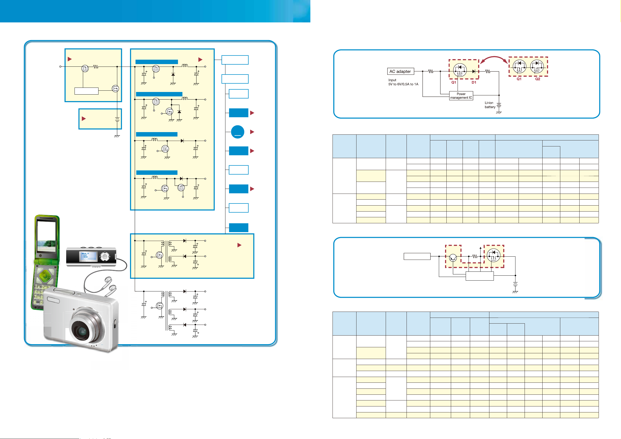
[GSM]
AC adapter
Input
5V to 6V/0.5A to 1A
Q1 D1
Power
management IC
MOSFETs (Pch) + Schottky Barrier Diodes (or MOSFETs (Pch))
Absolute maximum ratings/Ta=25˚C Electrical characteristics/Ta=25˚C
V
Q1+D1
Q1+Q2
/
Type No. Package 2 in 1
CPH5802 CPH5
VEC2822
VEC8
VEC2818
VEC2303
VEC2301 Pch MOS 20 ±10 3 0.9 0.087 0.120 - - -
VEC8
ECH8654
ECH8611 Pch MOS 12 ±9 5 1.3 0.045 0.065 - - -
❈
ECH8652 Pch MOS 12 ±10 6 1.3 0.031 0.045 - - -
ECH8
Pch MOS 20 ±10 2 0.9 0.140 0.200 - - -
SBD 15 - 1 - - - 1 0.35 0.4
Pch MOS 20 ±10 3.5 1 0.077 0.108 - - -
SBD 15 - 2 - - - 2 0.5 0.56
Pch MOS 20 ±10 3.5 1 0.077 0.108 - - -
SBD 30 - 2 - - - 2 0.45 0.5
Pch MOS 12 ±8 4 0.9 0.054 0.075 - - -
Pch MOS 20 ±10 5 1.3 0.041 0.058 - - -
DSS
V
R
[V]
V
GSS
[V]
ID/
I
[A]
O
[CDMA]
Q1
AC adapter
Input
5V to 6V/0.5A to 1A
Power
management IC
Li-ion
battery
P
D
[W]
Q1 Q2
RDS(on) [Ω]
VGS=2.5V
typ max typ max
Q2
Li-ion
battery
I
[A]
VF [V]
F
: Development
❈
Transistors (PNP) + MOSFETs (Pch)
Type No. Package 2 in 1
PNP TR 30 3 1.1 1.5 75 0.11 0.16 - -
Pch MOS 12 4 1.1 - - - - 0.054 0.074
PNP TR 30 3 1.1 1.5 75 0.11 0.16 - -
Pch MOS 20 3 1.1 - - - - 0.087 0.120
Q1+Q2
VEC2904
VEC8
VEC2905
Absolute maximum ratings/Ta=25˚C
V
/
CEO
V
DSS
[V]
IC/
I
[A]
D
P
P
[W]
C
D
I
[A]
Electrical characteristics/Ta=25˚C
(sat)
[V]
V
CE
C
I
B
[mA]
typ max typ max
: Development
❈
RDS(on) [Ω]
VGS=2.5V
CPH6122 CPH6 PNP TR 30 3 1.3 1.5 75 0.120 0.180 - -
❈
Q1
Q2
MCH6122 MCPH6 PNP TR 30 3 1.0 1.5 75 0.120 0.180 - -
❈
VEC1106 VEC8 PNP TR 30 5 1.4 1.5 75 0.105 0.155 - MCH6320
MCH6321 Pch MOS 20 4 1.5 - - - - 0.072 0.098
MCH6336 Pch MOS 12 5 1.5 - - - - 0.047 0.066
MCPH6
Pch MOS 12 5 1.5 - - - - 0.047 0.066
MCH6337 Pch MOS 20 4.5 1.5 - - - - 0.053 0.075
ECH8304
ECH8301 Pch MOS 20 8 1.6 - - - - 0.026 0.037
ECH8
Pch MOS 12 9.5 1.6 - - - - 0.018 0.026
EMH1303 EMH8 Pch MOS 12 7 1.5 - - - - 0.027 0.036
2
3
Page 4
Devices for Mobile Equipment
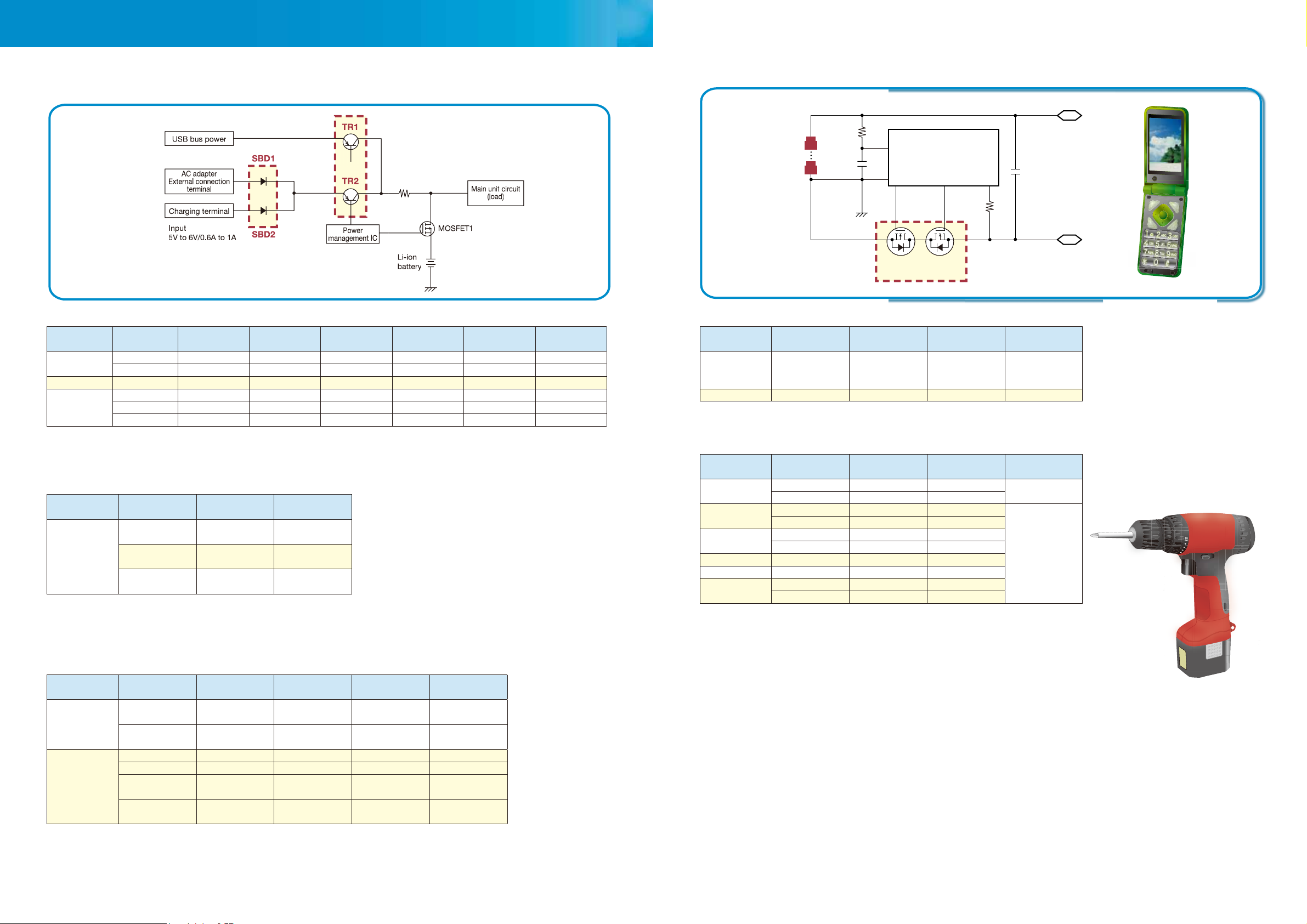
[CDMA]
TR1
USB bus power
SBD1
AC adapter
External connection
terminal
Charging terminal
Input
5V to 6V/0.6A to 1A
SBD2
TR2
Power
management IC
Li-ion
battery
MOSFET1
Main unit circuit
(load)
Li-ion Battery
■
B+
CELL
B-
P+
Control IC
P-
Battery Protection
Recommended Bipolar Transistors (PNP)
V
CEO
[V]
-12
-15 6.0 CPH3107
-30
I
C
[A]
MCPH3 MCPH6 CPH3 CPH6 VEC8 VEC8(2 in 1)
2.5 MCH3143 CPH3143
3.0 MCH3106 CPH3121 CPH6121
2.0 MCH3144 CPH3144
❈
3.0 MCH3109
MCH6122 CPH3122 CPH6122 VEC2102
5.0 CPH3110
Recommended Schottky Barrier Diodes (Single)
[Features]
• Package size: 1.6×0.8mm and IO=1A, Minimum in industry size !
• Thickness of Package: Typ. 0.60mm
V
[V]
30
R
I
[A]
0.2
0.5
1.0
O
ECSP1008-2 ECSP1608-4
SS0203EJ
SB0203EJ
SS0503EC SS0503EJ
SB0503EC SB0503EJ
SS1003EJ
SB1003EJ
Recommended Schottky Barrier Diodes (2 in 1: Parallel type)
[Features]
• Package size: 2.8×2.9mm and 30V/3A [SBS813/SBE813]
• Package size: 2.0×2.1mm and 30V/2A [SBS818], 15V/2A [SBS817]
• Thickness of Package: Typ. 0.75mm
V
[V]
15
30
R
I
O
[A]
1.0
2.0
MCPH5 EMH8 CPH5 VEC8
SBS808M SBS804
SBE808
SBS817
❈
SBE817
0.5 SBS806M SBE805
1.0
2.0
❈
SBS810 SBE807 SBS814
SBS818 SBS811
❈
SBE818 SBE811
3.0
: Development
❈
SBS813
SBE813
❈
VEC1105
❈
VEC1104
❈
VEC1106
: Development
❈
Recommended MOSFETs (Nch)
V
DSS
[V]
EMH8 ECH8 TSSOP8 SOP8
EMH2405 ECH8601R FTD2011A FW231A
20
EMH2407 ECH8649 FTD2017R FW232A
ECH8651R
30 EMH2402 ECH8622R FTD2019A
Recommended MOSFETs for Machine Tools
V
DSS
[V]
30
45
60
75 Nch 2SK4065 2SK4165
80 Pch 2SJ686
100
Polarity SMP ZP Drive
Nch 2SK4163
Pch TM1829Z
Nch 2SK4164
Pch TM1831Z
Nch 2SK4066 2SK4044
Pch 2SJ683
Nch 2SK4045
Pch 2SJ684
1.8V Drive
4.0V Drive
4
5
Page 5
Devices for Mobile Equipment
DC-DC Converter/Load SW
■
(1) DC-DC Converter
Recommended MOSFETs
Back Converter
(Step Down)
Synchronous Back Converter
(Pch + Nch or Nch + Nch)
Boost Converter
(Step Up)
Package Type No.
SCH2809
SCH6
SCH2811 -30 830 4.0
MCH5815
MCPH5
MCH5818 530
MCH5805 -60 2300 50V/0.1A
CPH5812
CPH5815 290*
CPH5
CPH5818 490* 4.0
CPH5802
CPH5835 235 2.5
CPH5822 -30 290 4.0 30V/0.5A
VEC8
Package Type No.
VEC2811 -30 168 4.0 30V/2A
VEC2817 -12 62* 2.5 15V/3A
SCH1305 -12 310*
SCH6
SCH1406
SCH2806
SCH2816 440 4.0
MCH3317 -12 290*
MCPH3/5
MCH3456 15 160
MCH5811 20 210 15V/1A
MCH5819 30 520 4.0 30V/0.5A
CPH3321 -12 98* 1.8
CPH3/5
CPH3337 -30 77 4.0
CPH5809 30 90 2.5
CPH5805 30 150
Package Type No.
SCH2817 15 160
SCH6
SCH2806 20 210
SCH2819
SCH2808 560 4.0
MCH5826 15 160
MCPH5
MCH5811 20 210 15V/1A
MCH5809
MCh5819 520 4.0
CPH5803
CPH5811 63
CPH5
CPH5831 63 15V/2A
CPH5809
CPH5805 150
VEC8
VEC2813 20 66 1.8
VEC2816 30 99 4.0
V
V
V
DSS
[V]
-12
-12
-12
-20
DSS
[V]
20
DSS
[V]
30
30
20
30
RDS(on)
max [mΩ]
VGS=4V
(*: VGS=4.5V)
290* 1.8
290* 1.8
290*
145 1.8
RDS(on)
max [mΩ]
VGS=4V
(*: VGS=4.5V)
210
RDS(on)
max [mΩ]
VGS=4V
215 2.5
215 2.5
210
90 2.5
Drive
[V]
SBD
15V/0.5ASCH2810 530 2.5
15V/0.5A
4.0MCH5802 -30 1090 30V/0.5A
1.8
15V/2A
15V/0.5A
15V/1A
Drive
[V]
1.8
SBD
-
15V/0.5A
1.8
-
-CPH3313 -20 235 2.5
4.0
Drive
[V]
30V/0.5ACPH5819 30 520
SBD
1.8 15V/0.5A
30V/0.5A
1.8
15V/0.5A
30V/0.5A
1.8
4.0
15V/1A
30V/0.5ACPH5819 520
30V/2A
[Bipolar Transistor Use Example]
Step up chopper
V
IN
V
OUT
Step down chopper
V
IN
V
OUT
Bipolar Transistors + Schottky Barrier Diodes
Absolute maximum ratings/Ta=25˚C
TR SBD TR SBD
Type No. Package
CPH5706
V
I
P
V
CEO
[V]
[A]
C
C
[W]
RRM
[V]
I
[A]
O
30 1.5 0.9 30 0.7 2 0.1 200 560 0.75 15 0.25 0.375 0.7 0.55 10 200 0.1 10
V
[V]
CE
IC
[A]
h
FE
min max
CPH5705 30 3 0.9 15 1 2 0.5 200 560 1.5 30 0.155 0.23 0.5 0.35 6 500 0.1 15
CPH5
CPH5702 30 3 0.9 30 0.7 2 0.5 200 560 1.5 30 0.12 0.18 0.7 0.55 15 80 0.1 10
CPH5703 50 3 0.9 50 0.5 2 0.1 200 560 1 50 0.08 0.12 0.5 0.55 25 50 0.1 10
Electrical characteristics/Ta=25˚C
VCE (sat) [V] VF [V] IR [
IC
[A]
IB
[mA]
typ max
I
[A]
F
max
VR
[V]
μ
A] t
max
rr
IF
[A]
Bipolar Transistors (PNP)
Absolute maximum ratings/Ta=25˚C Electrical characteristics/Ta=25˚C
Type No. Package
MCH3144
MCH3109 30 3 0.8 *
MCH3145 50 2 0.8 *
MCPH3
V
CEO
[V]
I
[A]
C
30 2 0.8 *
MCH3105 50 3 0.8 *
*1: When mounted on ceramic substrate (600mm2×0.8mm)
P
[W]
h
C
1
1
1
1
FE
min max
IC
[A]
200 560 1.5 75 0.17 0.26 MCH3244
200 560 1.5 30 0.155 0.23 MCH3209
200 560 1 50 0.165 0.33 MCH3245
200 560 1 50 0.1 0.2 MCH3205
VCE (sat) [V]
IB
[mA]
typ max
Bipolar Transistors (NPN)
Absolute maximum ratings/Ta=25˚C Electrical characteristics/Ta=25˚C
h
Type No. Package
MCH3244
MCH3221 *
MCH3245 50 2 0.8 *
MCH3222 *
*1: When mounted on ceramic substrate (600mm2×0.8mm) *2: MBIT III series (New Product)
2
MCPH3
2
V
CEO
[V]
I
[A]
C
30 2 0.8 *
30 3 0.8 *
50 3 0.8 *
P
[W]
C
1
1
1
1
FE
min max
200 560 1.5 75 0.16 0.24 MCH3144
250 400 1.5 30 0.08 0.12 200 560 1 50 0.13 0.26 MCH3145
250 400 1 50 0.06 0.09 -
B18 B22
Co
Ca
Co
IC
[A]
VCE (sat) [V]
IB
[mA]
typ max
[ns]
equivalent
max
+SB07-03C
+SB05-05CP
Internal
chip
product
CPH3115
+SBS006
CPH3109
+SBS004
CPH3209
CPH3205
Complementary
product
Complementary
product
Electrical
connection
B18
B18
B22
B22
EB
A
6
BECaA
7
Page 6
Devices for Mobile Equipment
(2) Load SW
Recommended MOSFETs
V
DSS
MCPH6 CPH6 VEC8 EMH8 Application Sample: Pch + Nch
LCD-Backlight
■
[Power MOSFET Use Example]
Push-Pull
Half-Bridge
Full-Bridge
20V MCH6628 CPH6605 - EMH2603
30V MCH6614 CPH6615 VEC2612 EMH2602
Power MOSFETs (Pch + Nch)
Absolute maximum ratings/Ta=25˚C Electrical characteristics/Ta=25˚C
Type No. Package Polarity
MCH6627
●
MCH6644
●
MCH6628
●
MCH6613
MCPH6
MCH6614
MCH6615
MCH6634
CPH6614
●
CPH6615
●
CPH6
CPH6605
CPH6610
VEC2602
●
VEC8
VEC2612
●
EMH2602
●
EMH8
EMH2603
●
SCH2602 SCH6
M07 M11 M12 M13 M26 M30
DSD
D1 G2 S2
V
DSS
[V]
V
GSS
[V]
Pch 30 20 1 0.8 0.42 0.55 0.72 1 75 2.6
Nch 30 20 1.4 0.8 0.23 0.3 0.4 0.56 65 2.5
Pch 30 20 1.2 0.8 0.32 0.42 0.59 0.83 104 3.3
Nch 30 20 1.8 0.8 0.16 0.21 0.3 0.42 95 3.2
Pch 20 10 1 0.8 0.38 0.5 0.54 0.76 115 1.5
Nch 30 10 0.35 0.8 2.9 3.7 3.7 5.2 7 1.58
Pch 30 10 0.2 0.8 8 10.4 11 15.4 7.5 1.43
Nch 30 10 0.35 0.8 2.9 3.7 3.7 5.2 7 1.58
Pch 30 10 0.4 0.8 2.4 3.1 3.5 4.9 28 2
Nch 30 10 0.35 0.8 2.9 3.7 3.7 5.2 7 1.58
Pch 30 10 0.4 0.8 2.4 3.1 3.5 4.9 28 2
Nch 30 10 0.65 0.8 0.9 1.2 1.2 1.7 30 2.34
Pch 30 10 0.4 0.8 1.5 1.9 2 2.8 40 0.83
Nch 30 10 0.7 0.8 0.7 0.9 0.8 1.15 30 1
Pch 30 20 1.2 0.8 0.32 0.42 0.59 0.83 104 3.3
Nch 30 20 1.8 0.8 0.15 0.195 0.29 0.41 95 3.2
Pch 30 20 1.8 0.9 0.18 0.235 0.32 0.45 226 5.5
Nch 30 20 2.5 0.9 0.079 0.105 0.15 0.21 187 5.2
Pch 20 10 1.5 0.8 0.18 0.235 0.24 0.34 40 3.2
Nch 30 10 0.65 0.8 0.9 1.2 1.2 1.7 30 2.34
Pch 30 9 0.4 0.8 1.4 1.8 2 2.8 40 0.83
Nch 30 20 1.4 0.8 0.245 0.32 0.415 0.58 65 2.5
Pch 30 20 3 0.9 0.065 0.086 0.117 0.168 510 11
Nch 30 20 4 0.9 0.037 0.048 0.07 0.099 370 8.5
Pch 30 20 3 0.9 0.073 0.095 0.115 0.161 180 4.9
Nch 30 20 3 0.9 0.065 0.086 0.117 0.168 510 11
Pch 30 20 2 1 0.053 0.069 0.105 0.15 280 6.4
Nch 30 20 3.5 1 0.115 0.15 0.215 0.31 285 6.7
Pch 20 10 2 1.1 0.165 0.235 0.26 0.52 420 5
Nch 30 10 0.15 0.6 3.7 5.2 6.4 12.8 7 2
Pch 12 10 1.5 0.6 - - 0.235 0.31 160 2.6
Nch 30 10 0.35 0.6 - - 2.9 3.7 7 1.58
I
D
[A]
DSD
[W]
N1
Controller
Controller
N2
CCFL
CCFL
: New products
●
P
D
VGS=10V VGS=4(4.5)V
typ max typ max
RDS (on) [Ω]
Ciss
[pF]
Qg
[nC]
Electrical
connection
M11
M11
M11
M11
M11
Power MOSFETs
Type No. Package Polarity
VEC2402 VEC8 Nch+Nch 30 99
ECH8402 Nch 30 32
ECH8
VEC2602
VEC8
VEC2612
ECH8609
ECH8402 Nch 30 32
ECH8
Nch+Nch 30 75
Pch 30 168
Nch 30 99
Pch 30 168
Nch 30 161
Pch 30 120
Nch 30 75
V
DSS
[V]
P1
N1
CCFL
RDS (on) max [mΩ]
(VGS=4V)
CCFL
Controller
V
IN
[V]
5 to 12
CCFL
Set size
[inch]
Small Screen
2.5 to 8
P2P1
Controller
N2N1
CCFL
Use example
Push-PullECH8606
Half-Bridge
Full-Bridge
ECH8302 Pch 30 48
M11
M11
M12
M12
[Bipolar Transistor Use Example]
Self-Excitation Type
V
IN
Q1
M07
M07
Q2
CCFL
M13
M13
M13
Bipolar Transistors
V
CES
Type No. Package Polarity
CPH5503
CPH5504 NPN+NPN 80 3
CPH5
NPN+NPN 40* 3
(*V
CBO)
[V]
I
[A]
C
V
IN
[V]
5 to 12
Set size
[inch]
Small Screen
2.5 to 8
Use example
Self-Excitation Type
D1 D1 D2
D1 D1 G1/D2
M30
M26
D1D2
S
GG
S1 G1 D2
GG
S
8
S1 G1D2S2 G2
S1 G2 S2
G1SG2
9
Page 7

Devices for Mobile Equipment
Flash Unit
■
[Use Example]
Battery
S/W element
Trans
Control IC
FRD
300V
Xe-tube
C
M
Trigger
transformer
IGBT
IGBT
DRIVER
Bipolar Transistors (NPN)
Absolute maximum ratings/Ta=25˚C Electrical characteristics/Ta=25˚C
h
Type No. Package Polarity
CPH3223
CPH3236 NPN 50 3 0.9 250 400 1 50 0.06 0.1
CPH
NPN 50 3 0.9 200 560 1 50 0.09 0.13
V
CEO
[V]
[A]
I
C
P
[W]
C
FE
min max
IC
[A]
VCE (sat) [V]
IB
[mA]
typ max
MOSFETs (Nch)
Absolute maximum ratings/Ta=25˚C
Type No. Package Polarity
MCH6422
●
MCH6424 Nch 60 10 3 1.5 - - 0.085 0.115 0.095 0.135 690 8.2
MCH6423 Nch 60 20 2 1.5 0.17 0.22 0.21 0.3 - - 220 6.4
●
MCPH6
V
DSS
[V]
V
GSS
[V]
I
[A]
P
D
[W]
D
VGS=10V VGS=4V VGS=2.5V
typ max typ max typ max
Nch 60 10 2 1.5 - - 0.17 0.22 0.19 0.27 325 4.2
Electrical characteristics/Ta=25˚C
RDS (on) [Ω]
Ciss
[pF]Qg[nC]
Bipolar Transistors (NPN) + MOSFETs (Nch)
Absolute maximum ratings/Ta=25˚C Electrical characteristics/Ta=25˚C
TR MOSFET TR MOSFET
Type No. Package
V
CEO
[V]
I
[A]
P
V
V
C
C
DSS
[W]
[V]
GSS
[V]
I
[A]
D
VEC2901 VEC8 50 5 1.1 30 10 0.15 0.25 250 400 26 1.6 53
P
[W]
D
h
FE
min max
Cob
typ
[pF]
VCE (sat) [V] RDS (on) [
IC
[A]
I
B
[mA]
typ max
0.055
VGS=4V
typ max typ max
0.11 2.9 3.7 3.7 5.2 7 1.58
Ω
]
VGS=2.5V
IGBT Drivers
IO+/IO-typ [mA]
VDD=5V VDD=2.5V
Type No. Package
V
DD
[V]
VIN / V
[V]
OUT
P
[W]
V
D
min
[V]
V
IH
max
[V]
IL
CL [pF] CL [pF]
TND721MH5 MCPH5 -0.3 to 7.5 -0.3 to VDD+0.3 0.8 2 1 5000 50 5000 10
: New products
●
Ciss
typ
[pF]
Qg
typ
[nC]
Condenser Microphone
■
[High-Frequency Devices Use Example]
Impedance transformation
diaphragm
Back plate
G
SD
Sound
The electric capacity changes
V
CC
V
OUT
Electric signal output
Mobile phone
Hands-free
Digital camera
Digital video camera
Portable games
other
High-Frequency Devices for Condenser Microphone
Absolute maximum ratings/Ta=25˚C Electrical characteristics/Ta=25˚C
V
Type No. Package
TF246
TF252 20 1 30 0.14 0.35 1.4 3.1 0.95 1.0 -102
TF202C
TF222B 20 1 100 0.14 0.35 1.4 5.0 1.1 -2.0 -102
USFP
TSSFP
TF218THC
TF208TH 20 1 100 0.14 0.35 1.4 5.0 1.1 -2.0 -102
VTFP
V
GDS
GDO
[V]
I
D
[mA]
P
D
[mW]
20 1 30 0.14 0.35 1.0 3.5 0.65 -3.0 -110
20 1 100 0.14 0.35 1.0 3.5 0.65 -3.0 -110
20 1 100 0.14 0.35 1.0 3.5 0.65 -3.0 -110
I
DSS
[mA]
min max
|yfs|
typ(*min)
[mS]
Ciss
typ
[pF]
Crss
typ
[pF]
G
typ
[dB]
V
TF252TH 20 1 100 0.14 0.35 1.4 3.1 0.95 1.0 -102
Type No.
Package
(unit: mm)
Absolute maximum ratings/Ta=25˚C
V
IN
[V]
V
DD
[V]
P
D
[mW]
V
DD
min max min max
Electrical characteristics/Ta=25˚C
[V]
Ci
typ
[pF]
I
DD
[μA]
G
[dB]
V
EC4K11KF ECSP1410 (1.4×1.0×0.4) ±0.5 4 100 2 3.6 2.7 140 100 12 -90
EC4K14MF ECSP1410 (1.4×1.0×0.32) ±0.5 4 100 2 3.6 2.7 140 200 12 -90
USB (3.3V) Signal Line Protection Devices
■
[Use Example]
D–
D+
Vbus
Shorted for use
USB
Controller
V
NO
max
[dB]
V
NO
[dB]
Flash Circuit IGBTs
Absolute maximum ratings/Ta=25˚C
V
Type No. Package Polarity
TIG030TS
●
TIG032TS Nch 400 ±6 180 10 1 0.4 1 150 2.5 3.4 4.8 10 1 5100
●
TSSOP8
V
CES
[V]
Nch 400 ±6 150 10 1 0.5 1.2 150 4 3.7 5.4 10 1 2610
GES
(DC)
[V]
I
CP
[A]
VGE(off) [V] VCE (sat) [V] Cies
I
V
C
CE
[mA]
[V]
Electrical characteristics/Ta=25˚C
IC
V
min max
[A]
GE
[V]
min max
V
[V]
CE
: New products
●
f
[MHz]
FRD
V
Type No. Package
V
[V]
R
I
O
[mA]
F
IF=0.1A
[V]
RE0208DA SOD-323 800 200 4.0 3 55
10
I
R
VR=400V
[μA]
IF=IR=100mA, See specifi ed test circuit
trr max
[ns]
typ
[pF]
Recommended Device
CT [pF]
f=1MHz/
VR=0V
Type No. Package
IR=1μA
min
VR [V]
IR=1mA
max
VF [V]
IF=1mA
IL [μA]
VR=2.5V
VS002E4 ECSP1608-4 3.4 4.0 0.35 1 16
typ
11
Noise clamping of USB eye patterns
Abnormal signals of 4.0V or more
eliminated (overshoot eliminated)
+D
–D
Abnormal signals of 0.35V or more
eliminated (undershoot eliminated)
Page 8

Devices for Mobile Equipment
Devices for Motor
■
[MOSFETs Use Example]
Devices for Fan Motor
Single-phase Motor (
Motor Driver
H-Bridge, Half pre.
LB11660V
): #5 Single-phase Motor (H-Bridge): #6 Three-phase Motor: #7
Q3
Q1
Q1
Q3
Q5
M M
Q1
Q2
Q2 Q4
Q2 Q4
Q6
MOSFETs
Absolute maximum ratings/Ta=25˚C
Type No. Package Polarity
MCH3410
MCH3421 Nch 100 20 0.8 0.9 0.68 0.89 0.85 1.2 165 4.8
MCPH3
Nch 30 20 2 0.9 0.115 0.15 0.19 0.27 120 3.6
V
DSS
[V]
V
GSS
[V]
I
[A]
P
D
D
[W]
VGS=10(15)V VGS=4(4.5)V
typ max typ max
MCH6423 MCPH6 Nch 60 20 2 1.5 0.17 0.22 0.21 0.3 220 6.4
CPH3418
CPH3424 Nch 60 20 1.8 1 0.17 0.22 0.21 0.3 220 6.4
CPH3
Nch 30 20 1.4 0.9 0.23 0.3 0.4 0.56 65 2.5
CPH3427 Nch 100 20 1 1 0.48 0.63 0.58 0.81 240 6.5
VEC2402 VEC8 Nch+Nch 30 20 4 0.9 0.037 0.048 0.07 0.099 370 8.5
CPH6616 CPH6 Nch+Nch 30 20 2.5 0.9 0.079 0.105 0.15 0.21 187 5.2
Electrical characteristics/Ta=25˚C
RDS (on) [Ω]
Ciss
[pF]Qg[nC]
MOSFETs (Pch+Nch)
Type No. Package Polarity
VEC2602 VEC8
ECH8609 ECH8
FW340
FW377
FW356
SOP8
FW359
FW360
Pch 30 20 3 0.9 0.065 0.086 0.117 0.168 510 11
Nch 30 20 4 0.9 0.037 0.048 0.07 0.099 370 8.5
Pch 30 20 4 1.3 0.05 0.067 0.087 0.12 550 2.2
Nch 30 20 6 1.3 0.025 0.034 0.052 0.075 510 11
Pch 30 20 5 1.8 0.041 0.053 0.07 0.098 1000 16.5
Nch 30 20 5 1.8 0.037 0.048 0.064 0.09 460 8.6
Pch 35 20 5 1.8 0.037 0.049 0.062 0.087 1224 24
Nch 35 20 6 1.8 0.025 0.033 0.043 0.061 1050 20
Pch 60 20 3.5 2 0.11 0.145 0.15 0.21 990 22
Nch 60 20 5 2 0.043 0.058 0.056 0.084 790 16
Pch 60 20 3 1.8 0.11 0.145 0.145 0.205 990 22
Nch 60 20 3 1.8 0.11 0.145 0.15 0.215 300 7.8
Pch 100 20 2 1.4 0.24 0.315 0.32 0.45 935 20
Nch 100 20 2 1.4 0.175 0.22 0.22 0.31 530 13
Absolute maximum ratings/Ta=25˚C
V
DSS
[V]
V
GSS
[V]
[A]
I
P
D
D
[W]
VGS=10V VGS=4(4.5)V
typ max typ max
Electrical characteristics/Ta=25˚C
RDS (on) [Ω]
Ciss
[pF]Qg[nC]
MOSFETs
Absolute maximum ratings/Ta=25˚C
Type No. Package Polarity
2SJ646
2SJ634 Pch 60 20 8 20 0.105 0.138 0.145 0.205 990 22
TP
Pch 30 20 8 15 0.058 0.075 0.097 0.136 510 11 #6, #7
V
DSS
[V]
V
GSS
[V]
[A]
I
P
D
D
[W]
VGS=10(15)V VGS=4(4.5)V
typ max typ max
2SJ637 Pch 100 20 5 20 0.24 0.312 0.32 0.45 935 20
2SK4067
2SK3492 Nch 60 20 8 15 0.115 0.15 0.155 0.22 300 7.8
TP
Nch 30 20 8 10 0.085 0.115 0.155 0.22 260 6 #6, #7
2SK3617 Nch 100 20 6 15 0.18 0.225 0.225 0.315 530 13
Electrical characteristics/Ta=25˚C
RDS (on) [Ω]
Ciss
[pF]Qg[nC]
M
Use
example
#5
Use
example
#6
#6, #7
#7
#6
#6, #7
Use
example
#7
#7
[Bipolar Transistor Use Example]
• For the purpose of power consumption reduction,
low saturated voltage transistor is recommended.
• PCP and TP packages with good radiation are
recommended.
• Composite type (B-E bias resistor, and C-E diode
V
IN
V
CC
are embedded) is recommended for miniaturization
purpose.
H
Hall element
GND
GND
Bipolar Transistors
Absolute maximum ratings/Ta=25˚C
Type No. Package Polarity
2SA2124
●
PNP 30 2 1.3 *
2SA2012 PNP 30 5 1.3 *
2SA2125 PNP 50 3 1.3 *
●
2SA2013 PNP 50 4 1.3 *
PCP
2SA1416 PNP 100 1 1.3 *
2SA1417 PNP 100 2 1.5 *
2SA2126
●
PNP 50 3 15 *
2SA2039 PNP 50 5 15 *
2SA2040 PNP 50 8 15 *
2SA2169 PNP 50 10 20 *
●
TP
2SA1592 PNP 100 1 10 *
2SA1593 PNP 100 2 15 *
V
CEO
[V]
I
[A]
C
P
[W]
C
min max
2
200 560 1.5 75 0.2 0.4 2SC6044
3
200 560 1.5 30 0.14 0.21 2SC5565
3
200 560 1 50 0.125 0.23 2SC5964
3
200 560 1 50 0.105 0.18 2SC5566
3
100 400 0.4 40 0.2 0.6 2SC3646
3
100 400 1 100 0.22 0.6 2SC3647
1
200 560 1 50 0.135 0.27 -
1
200 560 1 50 0.115 0.195 2SC5706
1
200 560 3.5 175 0.23 0.39 2SC5707
1
200 560 5 250 0.29 0.58 2SC6017
1
100 400 0.4 40 0.2 0.6 2SC4134
1
100 400 1 100 0.22 0.6 2SC4135
2SA1552 PNP 160 1.5 1 100 400 0.5 50 0.2 0.5 2SC4027
2
2SC6044
●
NPN 30 2 1.3 *
2SC5565 NPN 30 5 1.3 *
2SC5964 NPN 50 3 1.3 *
●
2SC5566 NPN 50 4 1.3 *
PNP
2SC3646 NPN 100 1 1.3 *
2SC3647 NPN 100 2 1.5 *
2SC5706
NPN 50 5 15 *
2SC5707 NPN 50 8 15 *
2SC6017 NPN 50 10 20 *
●
2SC4134 NPN 100 1 10 *
TP
2SC4135 NPN 100 2 15 *
200 560 1.5 75 0.17 0.26 2SA2124
3
200 560 1.5 30 0.125 0.19 2SA2012
3
200 560 1 50 0.1 0.15 2SA2125
3
200 560 1 50 0.085 0.13 2SA2013
3
100 400 0.4 40 0.1 0.4 2SA1416
3
100 400 1 100 0.13 0.4 2SA1417
1
200 560 1 50 0.09 0.135 2SA2039
1
200 560 3.5 175 0.16 0.24 2SA2040
1
200 700 5 250 0.18 0.36 2SA2169
1
100 400 0.4 40 0.1 0.4 2SA1592
1
100 400 1 100 0.13 0.4 2SA1593
2SC4027 NPN 160 1.5 1 100 400 0.5 50 0.13 0.45 2SA1552
*1: Tc=25˚C *2: When mounted on ceramic substrate (450mm2×0.8mm) *3: When mounted on ceramic substrate (250mm2×0.8mm)
Electrical characteristics/Ta=25˚C
h
FE
IC
[A]
[mA]
VCE (sat) [V]
IB
typ max
Complementary
Bipolar Transistors: Built-in Damper Diode
Absolute maximum ratings/Ta=25˚C
h
Type No. Package Polarity
2SB1397
2SB1325 PNP 20 4 1.5 *
PNP
PNP 20 2 1.3 *
V
CEO
[V]
[A]
I
C
P
[W]
C
2SB1324 PNP 30 3 1.5 *
2SB1739 TP PNP 30 3 1.5 *
●
2SD2100
2SD1999 NPN 20 4 1.5 *
PNP
NPN 20 2 1.3 *
2SD1998 NPN 30 3 1.5 *
2SD2720 TP NPN 30 3 1.5 *
●
*1: Tc=25˚C *2: When mounted on ceramic substrate (450mm2×0.8mm) *3: When mounted on ceramic substrate (250mm2×0.8mm)
FE
min
3
70 1 50 0.25 0.5 1.5 1.6
3
70 3 150 0.25 0.5 1.5 1.5
3
70 2 100 0.25 0.6 1.5 0.8
3
70 2 100 0.28 0.6 1.5 0.8
3
70 1 50 0.25 0.5 1.5 1.6
3
70 3 150 0.25 0.5 1.5 1.5
3
70 2 100 0.2 0.5 1.5 0.8
3
70 2 100 0.23 0.5 1.5 0.8
Electrical characteristics/Ta=25˚C
VCE (sat) [V]
IC
[A]
IB
[mA]
typ max
V
F
IF=0.5A
[V]
: New products
●
product
: New products
●
R
BE
(kΩ)
12
13
Page 9

Devices for SW Power Supply
Switching Power Supply Types & Recommended Power MOSFETs Map
■
Universal AC Input
20
Forward (1 or 2 used)
V
: 600to800V
DSS
Switching Devices
■
[MOSFET/FRD/SBD Use Example]
ACIN
FRD
[A]
D
14
Flyback
8
RCC or PWM
V
: 600 to 800V
DSS
Drain Current/I
6
30 50 100 150 200 250 300 350 400 450 500
Application Example
■
ACIN
PFC FRD
PFC
Control
PFC
MOSFET
(1) Flyback
For low-output use (up to 150W)
few externally-conneted parts required
1 MOSFET is used for switching
(2) Forward
Usable for middle-large ouput (100 to 300W)
Several switching MOSFETs can be used in parallel
Several switching MOSFETs can be used
(3) Half-Bridge
For middle output (<150 to 400W)
MOSFET with a lower voltage than flyback or
Forward voltage can be used
2 switching MOSFETs are used
(4) Full-Bridge
For high output (>300 to 400W)
MOSFET with a lower voltage than flyback or
forward voltage can be used
4 switching MOSFETs are used
Half-bridge (2 used)
V
: 450to500V
DSS
Output Power/P
V
CC
V
CC
V
Pulse IN
V
OUT
Main SW
MOSFET
Main Control
Main SW
MOSFET
Main Control
CC
Main SW
MOSFET
Main SW
MOSFET
CC
Full-bridge (4 used)
V
: 450to500V
DSS
[W]
When output becomes large, a high V
is required for the device
ex) Flyback Circuit
Output 80W → V
Output 120W → V
SBD
SBD
SBD
(3) Half-Bridge Circuit
SBD/FRD
SBD/FRD
(4) Full-Bridge Circuit
SBD
DSS
DSS
(1) Flyback Circuit
DC
Output
(2) Forward Circuit
DC
Output
Output
≥600V
≥700V
DC
DC
Output
DSS
PFC
Control
PFC
MOSFET
Main SW
MOSFET
SBD
SBD
(1) Power MOSFET/SBD/FRD for Adapter
Recommended Devices
Set Spec PFC Main SW Rectifi er
Applications/Power
Game machine
50W
Notebook PC
65W
General-purpose
75 to 90W
V
OUT
[V]
5 2.0 to 4.0
12 1.0 to 2.0 SBT100-16JS
20 2.0 to 4.0 -
5 2.0 to 4.0
12
24 SBT100-16JS
I
OUT
[A]
3.0 to 5.0
MOSFET MOSFET SBD
-
2SK4085LS
500V/0.33Ω
2SK4086LS
(600V/0.58Ω)
2SK4087LS
(600V/0.47Ω)
2SK4087LS
(600V/0.47Ω)
SBT80-04J
SBT100-16JS
SBT80-04J
SBT150-10JS
(2) Power MOSFET/SBD/FRD for other power supply
Recommended Devices [Other sets]
Set Specifi cation PFC Main SW Rectifi er
Set Specifi cation
Printer
BL DVD recorder Domestic (Japan) 100
DVD recorder Domestic (Japan) 60 - - 2SK4097LS SBT80-06J
Desktop PC W/W >200
PDP TV W/W >300
Domestic (Japan) 50 - - 2SK4096LS SBT150-10JS
W/W 50 - - 2SK4098LS SBT150-10JS
Power
[W]
FRD MOSFET MOSFET SBD
RD0506LS 2SK4097LS 2SK4087LS SBT100-16JS
❈
RD1006LS 2SK4085LS 2SK4125 SBT350-04J
❈
RD1006LS 2SK4124 2SK4124 SBT100-16JS
❈
DC
Output
❈
: Development
Main SW
MOSFET
14
SBD
15
Page 10

Devices for SW Power Supply
LCD TV
■
(3) Bipolar Transistors for Adapter
[Bipolar Transistor Use Example]
Output
AC Input
Bipolar Transistors [V
Type No. Package
Starting
resistor
R
BE
=700V/800V Series (AC Adapter)]
CBO
Absolute maximum ratings/Ta=25˚C
V
CBO
[V]
V
CEO
[V]
Main
S/W Tr
Thermistor
I
C
[A]
Electrical characteristics/Ta=25˚C
h
FE
IC
min max
[A]
[mA]
Control IC
VCE (sat) [V]
IC
IB
[mA]
2SC5823 TP 700 400 1.5 0.1 20 50 700 140 0.8 100/220 3/6
2SC5808 TP 700 400 2.5 0.3 20 50 1200 240 0.8 100/220 4/8
TT2240NMP NMP 700 400 1.0 0.1 15 30 500 100 0.8 100/220 1.5/3
❈
2SC6065-V NMP 700 400 1.5 0.1 20 50 700 140 0.8 100/220 3/6
2SC6083 SPA 700 350 1.0 0.1 100 200 500 100 0.8 100 1.5
2SC6083A SPA 700 400 1.0 0.1 50 100 500 100 0.8 100/220 1.5/3
2SC6146 SPA 800 350 1.0 0.1 100 200 500 100 0.8 220 3
❈
CPH3249 CPH3 700 350 1.0 0.1 100 200 500 100 0.8 100/220 1.5/3
CPH3249A CPH3 700 400 1.0 0.1 50 100 500 100 0.8 100/220 1.5/3
+5.6 to 5.8V/600 to 700mA
-
Input
Voltage
max
[V]
: Development
❈
AC Adapter
Circuits
[W]
Recommended Devices by LCD-TV Panel Size
(1) When BL inverter is half-bridge circuit, and AV output is fl yback circuit
ACIN
PFC
Control
PFC Circuit
PFC FRD(1)
V
CC
Pulse IN
Main SW
MOSFET(2)
SBD(2)/FRD(2)
PFC
MOSFET(1)
Main SW
MOSFET(2)
SBD(2)/FRD(2)
SBD(1)
SBD(1)
Main SW
MOSFET(3)
Main Control
Lineup
◆
SPS for
AV Processor
Panel Size
[inch]
Set Spec PFC
P
OUT
[W]
V
OUT
[V]
FRD(1) MOSFET(1) MOSFET(2) MOSFET(3)
2SK4086LS
up to 21 70 5/12 - -
(also used for
BL power supply)
26 to 32 150
37 to 42 250
at least 42 350
5 to 12
24
5 to 12
24
5 to 12
24/60
RD1006LS 2SK4085LS 2SK4098LS 2SK4096LS×2
❈
RD0506LS 2SK4124×2 2SK4098LS 2SK4097LS×2
❈
RD1006LS 2SK4124×3 2SK4101LS 2SK4084LS×2
❈
[Power supply block]
• Circuit
For under 21inch, used for both AV processor (main power supply) and BL inverter power supply.
For larger than 26inch, 2-power supply system is usually used (one is for BL inverter use, and the other is for AV processor use).
• Secondary-side diode voltage
In case of fl yback circuit, diode voltage should be 100V and above for 12V output (when PFC output is 380V).
In case of half-bridge circuit, diode voltage should be 100V and above for 24V output (when PFC output is 380V).
Half-Bridge Power Supply
Flyback Power Supply
DC
Output
* For under 21inch, also used for
BL inverter power supply.
SPS for
BL Inverter
-
DC
Output
: Development
❈
2nd Rectifi er
SBD(1)
SBD(2)/FRD(2)
SBT80-06J(1)
SBT100-16JS(1)
SBT100-16JS(1)
SBT100-16JS(2)
SBT100-16JS(1)
SBT150-10JS(2)
SBT100-16JS(2)
SBT150-10JS(1)
RD2004LS(2)
16
17
Page 11

Devices for SW Power Supply
(2)
The example when BL inverter adoptes PFC voltage direct input circuit, and AV output adopts fl yback circuit
(3) Devices for BL Inverter
1) Recommended Devices for Bridge Circuit
ACIN
PFC Circuit
PFC FRD(1)
PFC Direct input BL Inverter
PFC
Control
PFC
MOSFET(1)
Main SW
MOSFET(3)
Pulse IN
Driver
FRD(2)
FRD(2)
FRD(2)
FRD(2)
Multi CCFL, Parallel
CCFL
CCFL
CCFL
Main SW
MOSFET(3)
Flyback Power Supply for AV Processor
SBD
DC
Output
SBD
Main SW
MOSFET(2)
Main Control
Lineup
◆
Set Spec PFC Direct BL Inverter
Panel Size
[inch]
26 to 37 200 12
P
OUT
[W]
V
OUT
[V]
SPS for AV Processor
FRD(1) MOSFET(1) FRD(2) MOSFET(3) MOSFET(2) SBD
RD1006LS 2SK4085LS❈ RD0506LS 2SK4086LS×2 2SK4098LS SBT100-16JS
❈
: Development
❈
2nd Rectifi er
37 to 42 250 12 to 18❈ RD1006LS 2SK4124×2❈ RD0506LS 2SK4086LS×2 2SK4098LS SBT100-16JS×2
at least 42 350 12 to 18❈ RD1006LS 2SK4124×3❈ RD1006LS 2SK4085LS×2 2SK4101LS SBT100-16JS×2
Push-Pull Type
[Feature]
• Compared with half-bridge type, although doubled voltage is needed, meanwhile RDS(on) can be suppressed due to the use of Nch,
so a good symmetry can be achieved.
Because the current capacity is large, multi tubes driving can be made possible, and the needed parts count can be reduced.
Set Size
[inch]
21 to 32
at least 32
2.5 to 8
15 to 19
at least 32
up to 12
15 to 24
15 to 24Nch 2SK3704 (60V/15mΩ)
at least 60Nch 2SK4096 (500V/710mΩ)
5 to 12
5 to 12
15 to 24
5 to 12
15 to 24
at least 120Nch 2SK3092 (400V/2.3Ω)
Controller
Contoller
Separately-excitation Package Polarity Type No.
Nch 2SK3285 (30V/34mΩ)
N1
VIN
SMP
Nch 2Sk3352 (30V/21mΩ)
Nch 2SK3816 (60V/41mΩ)
Nch 2SK3818 (60V/18mΩ)
Nch 2SK2592 (250V/200mΩ) at least 60
Nch 2SK3703 (60V/28mΩ)
CCFL
TO-220ML
TO-220FI
Nch 2SK2160 (200V/350mΩ)
Nch 2SK2161 (200V/250mΩ)
N2
Nch 2SK4084 (500V/400mΩ)
VEC8
(VECxxxx)
ECH8
(ECH8xxx)
TSSOP8
(FTSxxxx(single))
(FTDxxxx(Dual))
Nch + Nch VEC2402 (30V/99mΩ)
Nch + Nch ECH8606 (30V/75mΩ)
Nch ECH8402 (30V/32mΩ)
Nch + Nch FTD8009 (30V/33mΩ)
Nch + Nch ECH8616 (60V/133mΩ) 15 to 24
Nch + Nch FW241 (30V/150mΩ)
Nch + Nch FW261 (30V/83mΩ)
Nch + Nch FW803 (30V/27mΩ)
N1
Nch FSS250 (30V/54mΩ)
Nch FSS804 (30V/20mΩ)
SOP8
(FSSxxxx(single))
(FWxxxx(Dual))
Nch + Nch FW808 (30V/37mΩ)
Nch + Nch FW250 (60V/215mΩ)
Nch + Nch FW256 (60V/84mΩ)
Nch FSS273 (45V/34mΩ)
Nch+Nch FW248 (45V/42mΩ)
N2
Nch FSS275 (60V/62mΩ)
Nch + Nch FW257 (100V/220mΩ)
Nch + Nch FW225 (450V/11.2Ω) at least 120
CCFL
CCFL
Nch SFT1402 (35V/40mΩ)
Nch SFT1403 (35V/25mΩ)
Nch 2SK3352 (30V/21mΩ)
Nch SFT1407 (45V/29mΩ)
TP
SMP
Nch SFT1405 (45V/74mΩ)
Nch 2SK3615 (60V/85mΩ)
Nch 2SK3816 (60V/41mΩ)
Nch 2SK3818 (60V/18mΩ)
Nch 2SK1920 (250V/700mΩ)
Nch 2SK3850 (600V/18.5Ω)
V
IN
[V]
18
19
Page 12

Devices for SW Power Supply
Full-bridge Type, Half-bridge Type
[Feature: Full-bridge/Half-bridge Type]
• Pch/Nch drive
• A large current device can drive multi tubes, thus the needed parts count can be reduced.
[Feature: Half-bridge Type (High voltage input)]
• A highly effi ective system can be achived by using a high side driver, whitch can make the inverter cicuit to be operated at a PFC
voltage level.
MOSFET should be Nch type and withstand a high voltage.
Separately-excitation Package Polarity Type No.
Full-Bridge
Controller
CCFL
CCFL
Half-Bridge (Nch + Pch)
P1
Controller
N1
Half-Bridge
P1
Controller
N1
Half-Bridge (High +B Voltage)
VIN(Low)
P1
Driver TND5XX
N1
CCFL
CCFL
P2P1
N2N1
CCFL
VIN(High)
CCFL
SMP
Controller
TO-220ML
TO-220FI
VEC8
(VECxxxx)
ECH8
(ECH8xxx)
SOP8
(FSSxxxx(single))
(FWxxxx(Dual))
SMP
TP
Nch 2SK3815 (60V/55mΩ)
Pch 2SJ659 (60V/133mΩ)
Nch 2SK3819 (100V/130mΩ)
Pch 2SJ664 (100V/136mΩ)
Nch 2SJ3702 (60V/55mΩ)
Pch 2SJ650 (60V/135mΩ)
Nch 2SK3706 (100V/130mΩ)
Pch 2SJ655 (100V/136mΩ)
Nch 2SK2161 (200V/350mΩ)
Pch 2SJ405 (200V/500mΩ)
Nch 2SK4096 (500V/710mΩ)
Nch 2SK4084 (500V/400mΩ)
Nch + Pch
Nch + Pch
VEC2602 (30V/99•168mΩ)
ECH8609 (30V/75•120mΩ)
Nch ECH8402 (30V/32mΩ)
Pch ECH8302 (30V/48mΩ)
Nch + Nch ECH8616 (60V/133mΩ)
Pch + Pch ECH8615 (60V/295mΩ)
Nch + Pch FW344 (30V/150•147mΩ)
Nch + Pch FW340 (30V/83•98mΩ)
Nch + Pch FW342 (30V/52•98mΩ)
Nch FSS802 (30V/26mΩ)
Pch FSS163 (30V/31mΩ)
Nch + Pch FW349 (30V/84•106mΩ)
Nch + Pch FW359 (30V/215•205mΩ)
Nch FSS273 (45V/34mΩ)
Pch FSS145 (45V/40mΩ)
Nch 2SK3351 (30V/21mΩ)
Pch 2SJ646 (30V/154mΩ)
Nch 2SK3285 (30V/34mΩ)
Nch 2SK3352 (30V/21mΩ)
Nch SFT1402 (35V/69mΩ)
Pch SFT1302 (35V/111mΩ)
Nch SFT1405 (45V/74mΩ)
Pch SFT1305 (45V/147mΩ)
Nch 2SK3615 (60V/85mΩ)
Pch 2SJ635 (60V/92mΩ)
Nch 2SK3818 (60V/18mΩ)
Pch 2SJ662 (60V/38mΩ)
Nch 2SK3979 (200V/450mΩ)
Pch 2SJ679 (200V/980mΩ)
Nch 2SK1920 (250V/700mΩ)
Pch 2SJ281 (250V/2Ω)
Set Size
[inch]
at least 32
at least 32
2.5 to 8
15 to 19
at least 32
V
IN
[V]
12 to 24
at least 60
12 to 24
at least 60
5 to 12
15 to 24
5 to 12
15 to 24
5 to 12
15 to 24
at least 120
Self-excitation Type (collector resonance)
[Feature]
• Multi tubes can be driven by using a power device with large current capacity.
also, the number of inverter circuits and used parts can be reduced.
→
• 4 to 8 tubes can be driven by circuit.
• Best choice for low-cost sets.
Self-excitation Package Type No.
V
IN
2SC5915 (120V/10A)
SMP
Q1
Q2
CCFL
TO-220ML
TO-220FI
2SC5999 (120V/25A)
2SC5888 (80V/10A)
2SC6080 (80V/13A) up to 15V
2SC5264 (800V/5A) at least 100V
2) Recommended Power MOSFETs & Bipolar Transistors by Monitor Size
[Power MOSFET Lineup by Input Voltage and Monitor Size]
PCP Package
V
Type No.
2SK3614 60 4
2SK3944 60 2
2SJ632 60 2
2SK3489 30 8
2SK3490 30 8
2SJ616 30 6
DSS
[V]
I
[A]
D
SOP8 Package
V
Type No.
FW250 60 3
FW359 60 3
FW248 45 6
FW349 45 4
DSS
[V]
I
[A]
D
Monitor Size [inch] (Standard)
20 32
[Bipolar Transistor Lineup by Input Voltage and Monitor Size]
VEC8 Package
V
Type No.
CES
[V]
VEC2202 120 2.5
VEC2201 100 3
CPH3 Package
V
Type No.
CPH3252 180 2
CPH3251 150 2
CPH3247 120 2.5
CPH3239 100 5
CPH3236 100 3
CPH3223 100 3
CES
[V]
[A]
[A]
I
C
I
C
PCP Package
V
Type No.
PCP1201 150 2.5
PCP1202 180 2
2SC6095 120 2.5
2SC6096 120 2
2SC3647 120* 2
2SC5991 100 7
2SC5990 100 4
2SC5964 100 3
2SC5994 100 2
CES
*VCBO
[V]
I
[A]
C
TP Package
V
Type No.
2SC6071 120 10
2SD1816 120* 4
2SD1815 120* 3
2SC6098 120 2.5
2SC6099 120 2
2SC5980 100 8
2SC5979 100 5
2SC5707 80 8
2SC5706 80 5
2SC6022 40* 9
2SC6020 40* 6
CES
*VCBO
[V]
Monitor Size [inch] (Standard)
820 32
Set Size
[inch]
at least 32 15 to 24V
up to 15V
at least 32
TP Package
V
Type No.
DSS
[V]
2SK3978 200 4
2SK3977 100 4
SFT1202 180 2
SFT1201 150 2.5
SFT1305 45 10
SFT1307 45 14
SFT1405 45 10
SFT1407 45 14
SFT1403 35 11
SFT1402 35 14
SMP Package
V
I
[A]
C
Type No.
2SC5974 700 7
2SC5999 120 25
2SC5915 120 10
CES
[V]
I
[A]
V
IN
[V]
D
I
C
[A]
20
21
Page 13

Devices for SW Power Supply
(4) Devices for Power MOSFET Buffer
1) Low Side Driver ExPD [MOSFET, IGBT Gate driver IC]
[Application]
• PDP, LCD-backlight, inverter light, liquid crystal projector, HID drive, motor drive, half-bridge/full-bridge power supply, etc.
[ExPD Use Example]
• Withstand voltage of 25V is assured.
• 2 low side drivers in
• TTL/CMOS compatible
(VIH=2.6V or less at VDD=4.5 to 25V)
• High-speed switching time
(tr/tf=typ 25ns, at 1000pF load [TND301S])
INA
OUTA
TND3xx
Control IC
INB OUTB
Load
(Inverter)
(Buffer)
MOSFET 1
Load
MOSFET 2
ExPDs
V
max
Type No. Package Functions
TND321VD
TND322VD Dual buffer 25 0.2 4.5 to 25 0.8 1 2.6 0.8
VEC8
Dual inverter 25 0.2 4.5 to 25 0.8 1 2.6 0.8
DD
[V]
PD max
[W]
Operating
voltage range
[V]
TND323VD Inverter buffer 25 0.2 4.5 to 25 0.8 1 2.6 0.8
TND307TD
TND308TD Dual buffer 25 0.25 4.5 to 25 1 1 2.6 0.8
TSSOP8
Dual inverter 25 0.25 4.5 to 25 1 1 2.6 0.8
TND309TD Inverter buffer 25 0.25 4.5 to 25 1 1 2.6 0.8
TND301S
Dual inverter 25 0.3 4.5 to 25 2 2 2.6 0.8
TND302S Dual buffer 25 0.3 4.5 to 25 2 2 2.6 0.8
TND303S Inverter buffer 25 0.3 4.5 to 25 2 2 2.6 0.8
TND304S Dual inverter 25 0.3 4.5 to 25 1 1 2.6 0.8
TND305S Dual buffer 25 0.3 4.5 to 25 1 1 2.6 0.8
TND306S Inverter buffer 25 0.3 4.5 to 25 1 1 2.6 0.8
TND311S Dual inverter 25 0.3 4.5 to 25 2 2 2.6 0.8
SOP8
TND312S Dual buffer 25 0.3 4.5 to 25 2 2 2.6 0.8
TND313S Inverter buffer 25 0.3 4.5 to 25 2 2 2.6 0.8
TND314S Dual inverter 25 0.3 4.5 to 25 1 1 2.6 0.8
TND315S Dual buffer 25 0.3 4.5 to 25 1 1 2.6 0.8
TND316S Inverter buffer 25 0.3 4.5 to 25 1 1 2.6 0.8
* TND30x series: input terminal Hi Z (high impedance); TND31x/TND32x series: input pull-down resistor in.
Drive capability
Source [A] Sink[A]
V
min
IH
[V]
V
IL
[V]
max
2) High Voltage Driver ExPD
[ExPD Use Example]
• High withstand voltage driver (600V)
• Under-voltage protection function is built in
ExPDs
V
Type No. Package
TND516SS
●
TND507S 600 250 500
SOP8
TND508S 600 250 500
TND512MD
●
TND505MD 600 250 500
MFP16
TND506MD 600 250 500
S
Source
[V]
[mA]
600 200 400 Single-phase high side driver
600 200 400 3-phase high side driver 3-phase motor drive applicatioon
HIN
L
SD
Control IC
LIN
I
O
Sink
[mA]
HOUT
MOSFET 1
TND506MD
VS
LOUT
Features Applications
MOSFET 2
Load
Ballasts, PDP maintenance drive, DC/AC
motor drive, induction heaters, charging
Single input/two output half bridge
driver circuits
Two input/output half bridge driver
circuits.
Built-in shutdown function and
low-side priority circuit.
Two input/output half bridge driver
circuits.
Built-in shutdown function.
circuits, high-frequency switching power
supplies, switching amplifi ers, and other
general-purpose driver applications
PDP maintenance drive, DC/AC motor
drive, ballasts, charging circuits,
high-frequency switching power supplies,
induction heaters, switching amplifi ers,
and other general-purpose driver
applications
22
23
Page 14

Devices for SW Power Supply
3) LCD-Backlight Inverter: ExPD
[TND3xx Use Example: MOSFET Driver]
Half-Bridge MOSFET Full-Bridge MOSFET Push-Pull MOSFET
TND3xx
V
V
DD
TND3xx
GND
P1
N1
CCFL
DD
GND
TND3xx
V
DD
GND
P1
N1
CCFL
P2
N2
V
DD
TND3xx
GND
[TND3xx Use Example: High-side FET Drive, Various Applications]
12V Power Supply Variation 24V Power Supply Variation
24V 24V
TND3xx
12V
P1
N1
12V
TND3xx
P1
N1
TND3xx
N1
N2
P1
CCFL
5) Air conditioner fan motor drive: ExPD
[TND512MD Use Example]
VM
GND
V
CC
C1
1000μF
C3
10μF
Z3
DZD6.8
C2
104
1.1kΩ
470Ω
C6
682C5682C4682
C16
104
T1
UOUT
T2
C23
472
R8 R7 R9 R10 R11 R12 R4
C10
105
16
15 14 13 12 11 10 9
D1 D2
TND512MD
1
2 34567 8
D3
VOUT
C24
C11
105
C13
105
472
C17
T4
T4
C12 105
104
WOUT
C25
472
T5
T6
C18
104
GND
4) PDP Sustain Driver: ExPD
[TND5xx, TND3xx Use Example]
TND3XX
INA
OUTA
INB
OUTB
V
GND
DD
R5
R6
C0
Control IC
D2
D3
GND
TND5XX
HOUT
V
DD
HIN
SD
LIN
LOUT
VH
HFG
VL
GND
C3
D1
R3
R4
R1
R2
N
GND
12V
N1
1
23456789101112131415
LB11696V
CTL
2928272625242322212019181716
30
C19
104
C21
104
T1 to T6: 2SK2624
D1 to D3: DFD05TC
PDP Panel
Vp
Cp
R21
10kΩ
R22
100kΩ
R23
100kΩ
C8
104
C7
182
RD
C9
4.7μF
R24
20kΩ
PWMIN HP
J4 J5
F/R
J6 J7
R24
20kΩ
24
25
Page 15

Devices for SW Power Supply
[Proposal]
1. Simplification of circuits
2. Common-ization of circuits
3. Helps reduce designing time
6) Bipolar Transistors: Separately-excited Inverter (MOSFET for Gate Drive)
[Bipolar Transistor Use Example]
• IC with large IC is recommended for driving large-capacitance MOSFET
• Composite type (PNP+NPN) is recommended for miniaturization purpose
Push-PullFull-Bridge
V
P
[W]
GND
C
DD
Buffer TR
Buffer TR
V
CE
[V]
N1
N2
Electrical characteristics/Ta=25˚C
h
FE
IC
min max
[A]
V
DD
Buffer TR
Buffer TR
V
GND
DD
Buffer TR
Buffer TR
GND
Bipolar Transistors
Type No. Package Polarity
MCH5541 MCPH5
MCH6542
MCPH6
MCH6545
CPH5541
CPH5506
CPH5516
CPH5518
CPH5524
CPH5
P1
P2
N2
N1
CCFL
Absolute maximum ratings/Ta=25˚C
V
CEO
[V]
I
[A]
I
C
CP
[A]
PNP 30 0.7 3 0.5 2 0.01 200 500 0.2 10 0.11 0.22
NPN 30 0.7 3 0.5 2 0.05 300 800 0.2 10 0.085 0.19
PNP 30 0.3 0.9 0.5 2 0.01 200 500 0.1 5 0.11 0.22
NPN 30 0.3 0.9 0.5 2 0.01 300 800 0.1 5 0.1 0.2
PNP 50 0.5 1 0.5 2 0.01 200 500 0.1 10 0.06 0.12
NPN 50 0.5 1 0.5 2 0.01 300 700 0.1 10 0.05 0.1
PNP 30 0.7 3 0.6 2 0.01 200 500 0.2 10 0.11 0.22
NPN 30 0.7 3 0.6 2 0.05 300 800 0.2 10 0.085 0.19
PNP 30 1.5 5 0.9 2 0.1 200 560 0.75 15 0.25 0.375
NPN 30 1.5 5 0.9 2 0.1 200 560 0.75 15 0.15 0.225
PNP 30 2 6 0.9 2 0.1 200 560 1.5 75 0.17 0.26
NPN 30 2 6 0.9 2 0.1 200 560 1.5 75 0.16 0.24
PNP 50 1 3 0.9 2 0.1 200 560 0.5 10 0.23 0.38
NPN 50 1 3 0.9 2 0.1 200 560 0.5 10 0.13 0.19
PNP 50 3 6 0.9 2 0.1 200 560 1 50 0.115 0.23
NPN 50 3 6 0.9 2 0.1 200 560 1 50 0.09 0.13
IC
[A]
CCFL
VCE (sat) [V]
IB
[mA]
Buffer Transistor Circuit
Buffer TR
Internal chip
equivalent
typ max
product
30A02MH
+30C02MH
30A01M
+30C01M
50A02CH
+50C02CH
30A02CH
+30C02CH
CPH3115
+CPH3215
CPH3144
+CPH3244
CPH3116
+CPH3216
CPH3123
+CPH3223
Electrical
connection
B14
B13
B13
B14
B14
B14
B14
B14
DC-DC Converter IC
■
TN8D41A/51A, TN5D41A/51A/61A: Separately-excited step-down switching regulator
[Functions/Features]
• Large current IO max 8A (TN8D41A/51A)
I
max 5A (TN5D41A/51A/61A)
O
• High effi ciency Vertical-type P-channel power MOSFET built-in
• High withstand voltage VIN max 57V
• Five external parts
Type No. Type Input voltage Output voltage/current Channels Power stage Package
• Built-in reference oscillator (150kHz)
• Built-in current limiter
• Built-in thermal shutdown circuit
• Built-in soft start circuit
• ON/OFF function (shared with soft start pin)
TN5D41A Step-down 10V to 40V 5V/5A 1ch Built-in (PMOS) TO-220FI5H-HB
TN8D41A Step-down 10V to 40V 5V/8A 1ch Built-in (PMOS) TO-220FI5H-HB
TN5D51A Step-down 20V to 48V 12V/5A 1ch Built-in (PMOS) TO-220FI5H-HB
TN8D51A Step-down 20V to 48V 12V/8A 1ch Built-in (PMOS) TO-220FI5H-HB
TN5D61A Step-down 30V to 48V 24V/5A 1ch Built-in (PMOS) TO-220FI5H-HB
[ExPD Use Example]
V
GND
V
IN
GND
1
Under Voltage
Protect
SS
5
SOFTSTART
2
Temperature
Protect
Band Gap
Over
OSC
Over Current
+
AMP
--
Protect
-COMP
+
Pch MOSFET
SENSE
OUTPUT
IN
+
SW
OUT
3
FB
4
+
[Application Example for Power Supply Makers: Allows High Design Freedom]
ACIN
PFC
Control
24V Output
V
OUT
GND
B13 B14
C1 B2
E1 B1E2C2
C2
B2
C1
5/3.3V
Output
ACIN
[Proposal]
1. Simplification of circuits
2. Common-ization of circuits
PFC
Control
3. Helps reduce designing time
24V Output
B1EC
26
27
TN5D/8D
Series
5to8AOutput
5/3.3V
Output
Page 16

Devices for Lighting
Inverter light
■
[Bipolar Transistor Use Example: Ball Lamp]
[MOSFET Use Example]
H
DB1
N
DB
R2
C2
Q1
NPN
C
+
C1
R
Q2
NPN
R
R
Bipolar Transistors
Absolute maximum ratings/Ta=25˚C
Type No. Package
TT2264
2SC6083A NPN 700 400 1 5 0.1 50 100 5 0.5
SPA
Polarity
V
CBO
[V]
V
CEO
[V]
I
[A]
C
NPN 700 400 0.3 5 0.03 50 100 5 0.15
TT2240NMP NMP NPN 700 400 1 1 0.1 15 30 5 0.5
TT2188
TT2146 NPN 500 400 8 5 0.8 20 50 5 4
TO-220
NPN 500 400 5 5 0.5 20 50 5 3
TT2196 NPN 500 400 12 5 1.2 20 50 5 6
Electrical characteristics/Ta=25˚C
1
h
FE
V
IC
CE
[V]
[A]
min max
V
CE
[V]
[MOSFET Use Example: Ball Lamp]
H
N
NFR1
C1
DB1
Q1
C4
+
C2
R4
ZD1 ZD2
C7
Q2
L1
Inductor
C5
hFE2
IC
[A]
Merit
at least 10 hFE of low current side is high
at least 10
at least 10
at least 10
at least 10
at least 10
C3R3 R2
hFE of low current side
is high, package is small
Package is small 20 to 60
tf=0.3μs 20 to 60
tf=0.3μs
tf=0.3μs
C5
C6
T1
L2
OUT1
OUT2
OUT3
OUT4
NTC1
PTC1
NTC2
power
up to 20
20 to 60
65 to 130
OUT1
OUT2
OUT3
OUT4
Set
[W]
D2
L1
D3
RD1006LS(600V/10A)
D4
Q2
V1
AC
for PFC circuit
+
+
C4C1
TND506
to
TND509
Control IC
Recommended Devices and Spec: Surface Mount Type
Recommended devices by inverter lighting set [AC=200V input]
Set output
(Fluorescent tube) [W]
32×2
40×2
86×2
PFC circuit Inverter circuit Remarks
2SK4136×2
2SK4181×2
2SK4137×2
2SK4182×2
2SK4138×2
2SK4183×2
2SK4136×2
2SK4181×2
2SK4136×2
2SK4181×2
2SK4138×2
2SK4183×2
525V device is recommended when a
larger margin is needed.
[ZP Package]
good surface radiation due to thin body
w
PD up better radiation than that of
SMP package. 10% PD up.
MOSFETs
Absolute maximum ratings/Ta=25˚C Electrical characteristics/Ta=25˚C
P
Type No. Package
2SK4136
●
2SK4137 500 30 9.5 80 0.5 0.65 750
●
2SK4138 500 30 14 100 0.4 0.52 1000
●
2SK4181 525 30 7.5 70 0.71 0.92 600
●
2SK4182 525 30 9 80 0.58 0.75 750
●
2SK4183 525 30 13 100 0.45 0.58 1000
●
ZP
V
DSS
[V]
V
GSS
[V]
I
[A]
D
500 30 8 70 0.65 0.85 600
D
Tc=25˚C
[W]
RDS (on) [Ω]
VGS=10(15)V
typ max
Recommended Devices and Spec: Lead Type
Recommended devices by inverter lighting set [AC=200V input]
Set output
(Fluorescent tube) [W]
40×2 2SK4186LS 2SK4198LS×2
86×2 2SK4186LS×2 2SK4199LS×2
86×3 2SK4187LS×2 2SK4187LS×2
PFC circuit Inverter circuit Remarks
[TO-220FI(LS) Package]
C3
: New products
●
Ciss
[pF]
for Inverter circuit use
(2 devices are used)
Q3
L2
C2
Q4
8.2
7.8
6.2
0.4
0.2
3
4.2
1
2
1.0
2.54
5.08
10.0
6.0
2.5
10.0
1
.
6
1
3.6
Light
Light
0.6
8.4
10.0
1.2
1.0
2.54
6.2
5.2
3.2
3.5
7.2
16.0
0.9
1.2
0.75
14.0
0.7
0.3
0.6
7.8
4.5
2.8
0.6
1.2
0.7
MOSFETs
Absolute maximum ratings/Ta=25˚C Electrical characteristics/Ta=25˚C
Type No. Package Polarity
2SJ281
2SK3979 Nch 200 30 6 20 0.32 0.45 - - 1090 18.2
●
PCP
V
DSS
[V]
V
GSS
[V]
I
[A]
D
P
[W]
D
VGS=10(15)V VGS=4(4.5)V
typ max typ max
Pch 250 30 3 30 1.5 2 - - 420 -
2SK1920 Nch 250 30 4 30 0.5 0.7 - - 420 -
28
RDS (on) [Ω]
Ciss
[pF]
: New products
●
Qg
[nC]
MOSFETs
Absolute maximum ratings/Ta=25˚C Electrical characteristics/Ta=25˚C
I
Type No. Package
2SK4098LS
●
2SK4099LS 600 30 8.5 35 0.72 0.94 815 -
●
2SK4086LS 600 30 11.5* 37 0.58 0.75 1000 38.2
●
2SK4087LS 600 30 14* 40 0.47 0.61 1200 46
●
TO-220FI(LS)
V
V
DSS
GSS
[V]
[V]
600 30 7 33 0.9 1.1 660 -
D
IDc*
[A]
P
D
Tc=25˚C
[W]
RDS (on) [Ω]
VGS=10(15)V
typ max
●
Ciss
[pF]Qg[nC]
29
: New products
2.55
123
2.4
2.55
Page 17

Devices for Lighting
Devices for Modem and Infrared Sensor
Emergency Lamp
■
[2SK4043LS Use Example]
FUSE
AC
T1
+
C1
Q2
Control IC
RS
+
Lamp
Q1
D9
MOSFETs
Absolute maximum ratings/Ta=25˚C Electrical characteristics/Ta=25˚C
P
Type No. Package
2SK4043LS TO-220FI(LS) 30 10 20 20 0.016 0.021 0.017 0.024 3000 37
●
HID Lamp
■
V
DSS
[V]
V
GSS
[V]
I
[A]
D
D
Tc =2 5 ˚C
[W]
VGS=2.5V VGS=4V
typ max typ max
RDS (on) [Ω]
Ciss
[pF]
[MOSFET Use Example]
VL=15V
FUSE
Battery
: New products
●
[nC]
Qg
Devices for Modem
■
[High-Voltage Transistor Use Example for MODEM Circuit]
High-voltage TR
TIP
Modular Jack
RING
Safety
&
Protection
High-voltage TR
High-voltage
Modem
Controller
TR
Transistors for Modem Circuit
Absolute maximum ratings/Ta=25˚C Electrical characteristics/Ta=25˚C
Type No. Package Polarity
V
CEO
[V]
I
[A]
C
P
[W]
C
FE
min max
f
T
typ
[MHz]
h
2SA1740 PCP PNP 400 0.2 1.3 60 200 70 50 5 0.8
2SA1699 NP PNP 400 0.2 0.6 60 200 70 50 5 0.8
2SA1785 NMP PNP 400 1 1 40 200 50 200 20 1
CPH3249A CPH NPN 400 1 0.6 50 100 20 10 100 0.8
●
2SC4548 PCP NPN 400 0.2 1.3 60 200 70 50 5 0.6
2SC4002 NP NPN 400 0.2 0.5 60 200 70 50 5 0.6
SOP8501 SOP8
*1: When mounted on ceramic substrate (250mm2×0.8mm)
PNP 400 1 1.3 40 200 70 0.2 20 1
NPN 400 0.2 1.3 60 200 70 0.05 5 0.6
IC
[mA]
VCE (sat) [V]
IB
[mA]
: New products
●
max
FRD
V
H
V
L
HOUT
TND507S
TND508S
IN
SD
GND
HFG
LOUT
GND
VCCReset
DISC OUT
Thre
Trig
LB8555
Timer IC
GND
MOSFETs
Absolute maximum ratings/Ta=25˚C Electrical characteristics/Ta=25˚C
P
Type No. Package
2SK4136 ZP 500 30 8 70 0.65 0.85 600 -
●
2SK2617ALS
●
2SK2618ALS 500 30 6.5 30 0.95 1.25 700 20
●
2SK2625ALS 600 30 5 30 1.5 2 700 20
●
2SK4098LS 600 30 7 33 0.9 1.1 660 -
●
TO-220FI(LS)
V
DSS
[V]
V
GSS
[V]
I
[A]
D
500 30 5 25 1.2 1.6 550 15
D
Tc=25˚C
[W]
RDS (on) [Ω]
VGS=10(15)V
typ max
Ciss
[pF]
: New products
●
Qg
[nC]
Devices for infrared sensor
■
[Junction FET Use Example]
Optical lens
Signal
(Infrared rays etc.)
Thermal energy
+
-
+
R
-
+
D
1
Sensor
2
S
G
3
Amplifier Comparator
Junction FET
Absolute maximum ratings/Ta=25˚C Electrical characteristics/Ta=25˚C
V
Type No. Package
EC3A04B ECSP1006-3B 30 30 10 100 0.6 3 5 4 1.1
●
V
DSX
[V]
V
GDS
GDO
[V]
I
D
[mA]
P
D
[mW]
I
DSS
[mA]
min max
|yfs|
typ
[mS]
Ciss
typ
[pF]
Output
Crss
typ
[pF]
Typical Applications
humanbody detection, temp.
detection, automatic switching, etc.
: New products
●
30
31
Page 18

Devices for Satellite/GPS
FM Transmitter
Satellite LNB
■
[Satellite LNB]
Frequency: 9 to 14GHz
RF IN
IF Amp.LNA.
MIX
IF OUT
Lo
LO
Ultrahigh-Frequency Transistors
Absolute maximum ratings/Ta=25˚C
f
Type No. Package
MCH4009
MCH4011 3.5 100 350 24 2 1.1 2 3 50 14.5 Lo/IF Amp.
MCH4012 3.5 200 500 20 2 1.0 2 3 100 12 Lo/IF Amp.
MCPH4
V
CEO
[V]
I
C
[mA]
P
C
[mW]
3.5 40 120 25 2 1.1 2 3 20 17 Lo/IF Amp.
T
typ
[GHz]
MCH4020 8 150 500 16.5 2 1.2 1 5 50 17.5 Lo/IF Amp.
High-Frequency Schottky Barrier Diodes
Absolute maximum ratings/Ta=25˚C Electrical characteristics/Ta=25˚C
Type No. Package
SBX201C CP 2 50 - 280 8.6 0.25 Mixer
●
GPS/XM Antenna Module
■
V
[V]
R
I
F
[mA]
P
[mW]
Electrical characteristics/Ta=25˚C
NF |S21e|
f
typ
[GHz]
V
[mV]
F
[dB]f[GHz]
Conversion Loss
[dB]
2
V
CE
[V]
I
C
[mA]
C
typ [pF]
typ
[dB]
: New products
●
[GPS/XM Antenna Module]
Frequency: 1.57 to 2.3GHz
RF IN
ANTENNA
MODULE
LNA.
ESD
LNA.
NAVIGATION
SECTION
IF Amp.MIX
IF
OUT
Lo
LO
High-Frequency Transistors
Absolute maximum ratings/Ta=25˚C
f
Type No. Package
MCH4009
MCH4011 3.5 100 350 24 2 1.1 2 3 50 14.5 LNA
MCH4012 3.5 200 500 20 2 1.0 2 3 100 12 LNA
MCPH4
V
CEO
[V]
I
C
[mA]
P
C
[mW]
3.5 40 120 25 2 1.1 2 3 20 17 LNA
T
typ
[GHz]
MCH4013 3.5 15 120 22.5 2 1.5 2 5 5 16 LNA
EC4H08C
EC4H09C 3.5 40 120 26 2 1.3 2 3 20 16.5 LNA
ECSP1008
3.5 15 50 24 2 1.5 2 3 10 17 LNA
Electrical characteristics/Ta=25˚C
NF |S21e|
f
typ
[GHz]
[dB]f[GHz]
2
V
CE
[V]
I
C
[mA]
typ
[dB]
Block
Block
Block
FM Transmitter
■
[Varactor Diode Use Example]
VCC=+14.4V (From cigarette Lighter in a car)
V_Reg
f_Ref
CONT.
3LN02M✕5
AS
CLK
DATA
ATT
PON
RF OUT
V
DD
LV2282VA
VCO
3.3V
Varactor Diode
Absolute maximum
ratings/Ta=25˚C
Type No. Package
V
[V]
R
V
[V]
R
C1 C2
min max
EC2C01C ECSP1008-2 15 1 18.5 21.5 4 3.5 4.5 5.0
SVC710 MCPH3 15 1 18.5 21.5 4 3.5 4.8 4.8
SVC707 SPA 15 1 18.58 21.26 4 3.61 4.73 3.0
Any and all SANYO Semiconductor Co.,Ltd. products described or contained herein are, with regard to
"standard application", intended for the use as general electronics equipment (home appliances, AV equipment,
communication device, office equipment, industrial equipment etc.). The products mentioned herein shall not
be intended for use for any "special application" (medical equipment whose purpose is to sustain life,
aerospace instrument, nuclear control device, burning appliances, transportation machine, traffic signal
system, safety equipment etc.) that shall require extremely high level of reliability and can directly threaten
human lives in case of failure or malfunction of the product or may cause harm to human bodies, nor shall they
grant any guarantee thereof. If you should intend to use our products for applications outside the standard
applications of our customer who is considering such use and/or outside the scope of our intended standard
applications, please consult with us prior to the intended use. If there is no consultation or inquiry before the
intended use, our customer shall be solely responsible for the use.
Specifications of any and all SANYO Semiconductor Co.,Ltd. products described or contained herein stipulate
the performance, characteristics, and functions of the described products in the independent state, and are
not guarantees of the performance, characteristics, and functions of the described products as mounted in the
customer's products or equipment. To verify symptoms and states that cannot be evaluated in an
independent device, the customer should always evaluate and test devices mounted in the customer's
products or equipment.
SANYO Semiconductor Co.,Ltd. assumes no responsibility for equipment failures that result from using
products at values that exceed, even momentarily, rated values (such as maximum ratings, operating
condition ranges, or other parameters) listed in products specifications of any and all SANYO Semiconductor
Co.,Ltd. products described or contained herein.
SANYO Semiconductor Co.,Ltd. strives to supply high-quality high-reliability products, however, any and all
semiconductor products fail or malfunction with some probability. It is possible that these probabilistic failures
or malfunction could give rise to accidents or events that could endanger human lives, trouble that could give
rise to smoke or fire, or accidents that could cause damage to other property. When designing equipment,
adopt safety measures so that these kinds of accidents or events cannot occur. Such measures include but
are not limited to protective circuits and error prevention circuits for safe design, redundant design, and
structural design.
In the event that any or all SANYO Semiconductor Co.,Ltd. products described or contained herein are
controlled under any of applicable local export control laws and regulations, such products may require the
export license from the authorities concerned in accordance with the above law.
No part of this publication may be reproduced or transmitted in any form or by any means, electronic or
mechanical, including photocopying and recording, or any information storage or retrieval system, or
otherwise, without the prior written consent of SANYO Semiconductor Co.,Ltd.
Any and all information described or contained herein are subject to change without notice due to
product/technology improvement, etc. When designing equipment, refer to the "Delivery Specification" for the
SANYO Semiconductor Co.,Ltd. product that you intend to use.
Information (including circuit diagrams and circuit parameters) herein is for example only; it is not guaranteed
for volume production.
Upon using the technical information or products described herein, neither warranty nor license shall be
granted with regard to intellectual property rights or any other rights of SANYO Semiconductor Co.,Ltd. or any
third party. SANYO Semiconductor Co.,Ltd. shall not be liable for any claim or suits with regard to a third
party's intellectual property rights which has resulted from the use of the technical information and products
mentioned above.
Electrical characteristics/Ta=25˚C
V
R
[V]
min max
∆Cm [%]
C1.0V/C4.0V
max
32
33
Page 19

Ordering number : EP124
SANYO Semiconductor Co.,Ltd. Website
http://www.semic.sanyo.co.jp/index_e.htm
This catalog provides information as of June, 2008.
Specifications and information herein are subject to change without notice.
SANYO Semiconductor Co., Ltd.
 Loading...