

Page 1
Ordering number : ENN6578
EC3H07B
NPN Epitaxial Planar Silicon Transistor
EC3H07B
UHF to S Band Low-Noise Amplifier
and OSC Applications
Features
•
Low noise : NF=1.5dB typ (f=2GHz).
• High cut-off frequency : f
• Low operating voltage.
• High gain : S21e
• Ultraminiature (1006 size) and thin (0.5mm) leadless
2
=10GHz typ (VCE=1V).
T
: fT=12.5GHz typ (VCE=3V).
=9.5dB typ (f=2GHz).
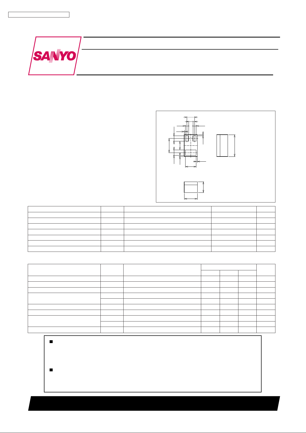
Package Dimensions
unit : mm
2183
0.05
0.25
0.35
0.2
0.15
1
[EC3H07B]
0.15
2
package.
3
0.5
0.6
0.05
0.05
0.5
0.4
0.65
0.25
0.05
(Bottom View)
Specifications
Absolute Maximum Ratings at Ta=25°C
Parameter Symbol Conditions Ratings Unit
Collector-to- Base Voltage V
Collector-to-Emitter Voltage V
Emitter-to-Base Voltage V
Collector Current I
Collector Dissipation P
Junction T emperature Tj 150 °C
Storage Temperature T stg --55 to +150 °C
CBO
CEO
EBO
C
C
1.0
1 : Base
2 : Emitter
3 : Collector
SANYO : E-CSP1006-3
9V
4V
2V
30 mA
100 mW
Electrical Characteristics at Ta=25°C
Parameter Symbol Conditions
Collector Cutoff Current I
Emitter Cutoff Current I
DC Current Gain h
Gain-Bandwidth Product
Output Capacitance Cob VCB=1V, f=1MHz 0.55 0.7 pF
Reverse Transfer Capacitance Cre VCB=1V, f=1MHz 0.4 pF
Forward Transfer Gain
Noise Figure NF VCE=1V, IC=3mA, f=2GHz 1.5 2.3 dB
CBO
EBO
FE
fT1VCE=1V, IC=5mA 8 10 GHz
fT2VCE=3V, IC=15mA 12.5 GHz
S21e
S21e
VCB=5V, IE=0 1.0 µA
VEB=1V, IC=0 10 µA
VCE=1V, IC=5mA 100 160
2
1VCE=1V, IC=5mA, f=2GHz 8 9.5 dB
2
2VCE=3V, IC=15mA, f=2GHz 10.5 dB
Any and all SANYO products described or contained herein do not have specifications that can handle
applications that require extremely high levels of reliability, such as life-support systems, aircraft's
control systems, or other applications whose failure can be reasonably expected to result in serious
physical and/or material damage. Consult with your SANYO representative nearest you before using
any SANYO products described or contained herein in such applications.
SANYO assumes no responsibility for equipment failures that result from using products at values that
exceed, even momentarily, rated values (such as maximum ratings, operating condition ranges, or other
parameters) listed in products specifications of any and all SANYO products described or contained
herein.
Ratings
min typ max
SANYO Electric Co.,Ltd. Semiconductor Company
TOKYO OFFICE Tokyo Bldg., 1-10, 1 Chome, Ueno, Taito-ku, TOKYO, 110-8534 JAPAN
72100 TS IM TA-2555
No.6578-1/6
Unit
Page 2
EC3H07B
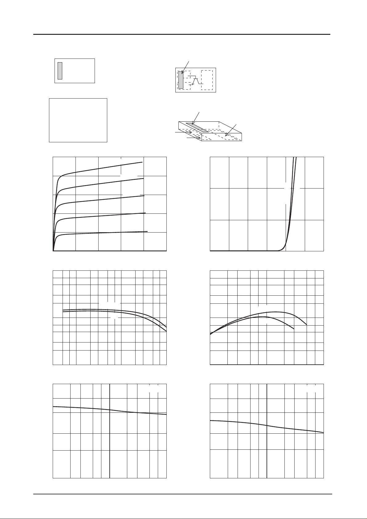
Type No. Indication (Top view) Electrical Connection (Top view)
Polarity mark (Top)
G
This product adopts a
high-frequency process.
Please be careful when
handling it beause it is
susceptible to static
electricity.
10
8
-- mA
C
6
4
Collector Current, I
2
0
0
1000
7
5
3
FE
2
100
7
5
DC Current Gain, h
3
2
10
357
1.0
7
1
Collector-to-Emitter Voltage, VCE -- V
1.0
I
C -- VCE
0.05mA
0.04mA
0.03mA
0.02mA
0.01mA
IB=0
32
h
FE -- IC
V
=3V
CE
1V
3
2
7
5
10 100
Collector Current, IC -- mA
Cob -- V
CB
2
4
3
f=1MHz
IT02240
5
IT02242
Base
Emitter
Base
5
7
Polarity mark (Top)
Emitter
Collector
*Electrodes : on the bottom
Collector
30
20
-- mA
C
10
Collector Current, I
0
0.2 0.4 0.6 0.8 1.0 1.2
0
Base-to-Emitter V oltage, VBE -- V
100
7
5
3
-- GHz
T
2
10
7
5
3
2
Gain-Bandwidth Product, f
1.0
1.0
2
3
Collector Current, IC -- mA
1.0
7
I
C -- VBE
fT -- I
=3V
V
CE
1V
57
10
Cre -- V
1V
=3V
CE
V
C
2357
CB
IT02241
100
IT02243
f=1MHz
Output Capacitance, Cob -- pF
0.1
5
3
2
5
3
2
Reverse Transfer Capacitance, Cre -- pF
0.1
2
5
3
7
1.0
Collector-to-Base Voltage, V
2
CB --
5
3
7
10
IT02244
V
0.1
0.1
2 3 57 2 3 57
Collector-to-Base Voltage, V
1.0
CB --
IT02245
V
10
No.6578-2/6
Page 3

EC3H07B
18
16
-- dB
14
2
12
10
8
6
4
2
Forward Transfer Gain, S21e
0
1.0
5.0
4.5
4.0
dB
3.5
--
3.0
2.5
2.0
1.5
Noise Figure, NF
1.0
0.5
0
1.0
S21e2 -- I
=3V
CE
V
1V
3
2
7
5
Collector Current, IC -- mA
NF -- I
V
CE
=3V
1V
532
7
Collector Current, IC -- mA
C
f=1GHz
3
2
10
7
5
100
IT02246 IT02247
C
f=2GHz
532
7
10
100
IT02248
18
16
-- dB
14
2
12
10
8
6
4
2
Forward Transfer Gain, S21e
0
1.0
120
100
-- mW
80
C
60
40
20
Collector Dissipation, P
0
23 5
0
S21e2 -- I
V
CE
C
=3V
1V
7
10
23 5
Collector Current, IC -- mA
P
-- Ta
C
4020
100 12060 80
Ambient Temperature, Ta -- °C
f=2GHz
7
140
IT02249
100
160
S Parameters (Common emitter)
VCE=1V, IC=1mA, ZO=50Ω
Freq(MHz)
200 0.970 --13.4 3.174 166.3 0.046 79.8 0.981 --10.3
400 0.939 --26.1 3.115 153.6 0.087 70.3 0.948 --19.9
600 0.892 --38.6 2.986 141.5 0.122 61.2 0.899 --28.4
800 0.839 --50.0 2.803 130.5 0.149 54.2 0.849 --36.1
1000 0.791 --59.7 2.596 121.8 0.171 48.5 0.798 --42.4
1200 0.739 --69.5 2.426 112.0 0.185 43.3 0.757 --48.6
1400 0.686 --77.7 2.210 104.5 0.195 39.7 0.708 --54.0
1600 0.649 --85.1 2.077 97.8 0.204 36.1 0.680 --58.0
1800 0.623 --91.6 1.987 90.9 0.210 33.3 0.651 --61.7
2000 0.595 --97.8 1.871 84.8 0.212 31.3 0.632 --65.1
2200 0.568 --104.1 1.768 78.9 0.213 30.0 0.617 --68.2
2400 0.542 --109.7 1.682 73.4 0.217 28.8 0.611 --72.5
2600 0.523 --114.6 1.593 68.4 0.212 27.9 0.579 --75.1
2800 0.505 --119.6 1.541 64.1 0.209 29.2 0.570 --75.8
3000 0.489 --124.1 1.468 60.2 0.216 31.2 0.604 --75.7
S
11
∠S
S
11
21
∠S
S
21
12
∠S
S
12
22
∠S
22
No.6578-3/6
Page 4

EC3H07B
VCE=1V, IC=5mA, ZO=50Ω
Freq(MHz)
200 0.859 --31.5 11.298 153.4 0.042 70.7 0.901 --22.4
400 0.740 --55.7 9.494 133.0 0.072 59.4 0.763 --38.4
600 0.619 --76.3 7.753 118.3 0.088 52.9 0.631 --49.6
800 0.546 --90.6 6.351 108.4 0.099 49.4 0.548 --56.1
1000 0.480 --104.5 5.414 100.0 0.108 48.0 0.471 --61.0
1200 0.443 --113.5 4.629 94.2 0.116 48.2 0.422 --64.5
1400 0.418 --121.2 4.063 88.7 0.124 48.6 0.399 --67.9
1600 0.393 --127.4 3.615 83.7 0.130 49.3 0.372 --70.3
1800 0.382 --132.4 3.292 79.3 0.140 49.9 0.356 --72.1
2000 0.372 --138.0 3.003 75.1 0.147 51.6 0.343 --74.1
2200 0.360 --143.3 2.764 71.2 0.157 51.9 0.333 --76.7
2400 0.352 --148.2 2.567 67.3 0.166 51.9 0.338 --79.6
2600 0.349 --152.4 2.408 63.9 0.173 52.6 0.310 --81.9
2800 0.348 --155.5 2.272 60.5 0.183 53.8 0.301 --83.5
3000 0.348 --158.1 2.154 57.7 0.194 53.9 0.293 --85.3
VCE=1V, IC=10mA, ZO=50Ω
Freq(MHz)
200 0.747 --46.5 15.679 144.0 0.039 66.9 0.807 --30.4
400 0.588 --77.7 11.464 122.1 0.059 55.5 0.614 --46.8
600 0.490 --98.9 8.634 108.9 0.072 51.8 0.485 --55.5
800 0.438 --114.0 6.882 99.9 0.082 52.0 0.410 --60.2
1000 0.404 --125.0 5.688 93.3 0.091 53.3 0.362 --62.9
1200 0.384 --133.1 4.844 87.9 0.100 55.0 0.330 --64.4
1400 0.371 --139.6 4.207 83.1 0.111 56.1 0.312 --67.3
1600 0.357 --145.5 3.734 78.6 0.121 56.4 0.299 --69.3
1800 0.350 --150.9 3.354 74.9 0.132 57.6 0.287 --70.4
2000 0.348 --155.0 3.069 71.0 0.141 58.8 0.280 --72.5
2200 0.344 --158.7 2.818 67.7 0.152 59.4 0.275 --75.6
2400 0.342 --163.1 2.615 64.0 0.165 58.9 0.280 --78.4
2600 0.341 --165.4 2.435 60.8 0.175 60.2 0.262 --79.9
2800 0.341 --168.4 2.287 57.9 0.187 60.5 0.257 --81.5
3000 0.349 --171.5 2.181 55.4 0.200 59.5 0.255 --83.7
S
11
S
11
∠S
∠S
S
11
11
21
S
21
∠S
∠S
S
21
21
12
S
12
∠S
∠S
S
12
12
22
S
22
∠S
∠S
22
22
VCE=1V, IC=20mA, ZO=50Ω
Freq(MHz)
200 0.598 --71.6 16.506 131.7 0.036 57.2 0.648 --37.6
400 0.476 --108.0 10.451 110.5 0.050 52.1 0.448 --50.7
600 0.429 --128.1 7.427 99.3 0.061 54.2 0.353 --55.1
800 0.410 --141.1 5.736 91.8 0.071 56.7 0.307 --57.5
1000 0.398 --149.3 4.699 85.9 0.080 58.4 0.282 --59.0
1200 0.393 --155.7 3.949 81.0 0.092 60.5 0.268 --60.1
1400 0.388 --160.9 3.420 76.7 0.104 61.9 0.265 --63.5
1600 0.383 --165.3 3.042 72.4 0.116 62.8 0.261 --65.4
1800 0.382 --169.0 2.726 68.7 0.126 63.5 0.261 --67.7
2000 0.382 --172.0 2.491 65.1 0.139 64.4 0.259 --70.2
2200 0.382 --175.0 2.294 61.9 0.152 65.1 0.258 --74.0
2400 0.381 --177.9 2.131 58.4 0.166 64.7 0.268 --77.5
2600 0.383 179.9 2.003 55.4 0.175 64.6 0.254 --80.2
2800 0.386 177.0 1.859 52.4 0.191 65.0 0.253 --82.3
3000 0.390 175.0 1.765 49.6 0.205 64.2 0.252 --85.1
S
11
∠S
S
11
21
∠S
S
21
12
∠S
S
12
22
∠S
22
No.6578-4/6
Page 5

EC3H07B
VCE=3V, IC=1mA, ZO=50Ω
Freq(MHz)
200 0.973 --12.2 3.240 167.1 0.040 80.6 0.984 --9.2
400 0.946 --24.1 3.185 155.4 0.077 72.0 0.957 --17.9
600 0.901 --35.8 3.049 144.0 0.108 63.2 0.915 --25.8
800 0.850 --46.4 2.870 134.1 0.133 56.5 0.871 --33.0
1000 0.813 --55.6 2.679 124.0 0.155 51.3 0.825 --39.1
1200 0.753 --64.9 2.493 116.4 0.167 46.1 0.784 --44.9
1400 0.713 --72.1 2.332 108.5 0.178 42.5 0.740 --49.7
1600 0.678 --79.4 2.215 100.4 0.188 39.1 0.713 --53.8
1800 0.643 --86.8 2.042 93.6 0.191 36.2 0.689 --57.5
2000 0.609 --92.9 1.916 87.7 0.195 34.4 0.670 --60.9
2200 0.581 --98.9 1.811 81.8 0.196 33.1 0.653 --64.1
2400 0.552 --104.5 1.726 76.4 0.200 32.3 0.646 --68.2
2600 0.530 --109.0 1.632 71.6 0.195 31.3 0.611 --70.8
2800 0.510 --113.8 1.552 67.4 0.194 33.0 0.601 --71.5
3000 0.493 --118.3 1.505 63.6 0.200 35.3 0.635 --71.4
VCE=3V, IC=5mA, ZO=50Ω
Freq(MHz)
200 0.876 --27.6 11.400 155.7 0.036 73.0 0.919 --19.4
400 0.756 --50.7 9.463 137.5 0.065 61.9 0.788 --34.8
600 0.634 --70.0 8.035 122.7 0.081 55.4 0.673 --44.7
800 0.555 --83.7 6.684 112.7 0.093 51.2 0.588 --50.8
1000 0.490 --95.2 5.807 103.8 0.101 50.0 0.515 --55.3
1200 0.450 --103.5 5.045 97.1 0.107 50.0 0.477 --58.1
1400 0.421 --111.2 4.444 91.5 0.116 50.3 0.442 --61.5
1600 0.392 --117.2 3.968 86.3 0.123 51.4 0.413 --63.7
1800 0.376 --123.2 3.601 82.0 0.131 52.0 0.393 --65.4
2000 0.359 --128.9 3.300 77.8 0.138 53.2 0.377 --67.3
2200 0.345 --133.9 3.026 74.3 0.149 53.9 0.360 --69.6
2400 0.336 --138.9 2.798 70.4 0.157 54.0 0.361 --72.2
2600 0.333 --142.0 2.636 66.9 0.164 54.2 0.335 --73.9
2800 0.329 --145.8 2.477 63.6 0.174 55.5 0.331 --74.9
3000 0.333 --148.6 2.369 60.7 0.184 55.7 0.327 --77.1
S
11
S
11
∠S
∠S
S
11
11
21
S
21
∠S
∠S
S
21
21
12
S
12
∠S
∠S
S
12
12
22
S
22
∠S
∠S
22
22
VCE=3V, IC=10mA, ZO=50Ω
Freq(MHz)
200 0.782 --38.7 16.264 148.0 0.034 68.7 0.853 --25.8
400 0.618 --67.3 12.556 126.5 0.055 58.7 0.671 --41.8
600 0.512 --86.2 9.670 113.1 0.067 55.8 0.544 --49.9
800 0.444 --101.0 7.790 103.6 0.077 54.5 0.462 --54.7
1000 0.398 --112.0 6.474 96.8 0.086 55.1 0.408 --57.2
1200 0.372 --120.3 5.540 91.1 0.096 56.5 0.373 --59.0
1400 0.352 --127.6 4.824 86.4 0.105 57.9 0.351 --61.1
1600 0.333 --133.0 4.287 82.0 0.115 58.3 0.334 --62.8
1800 0.323 --139.0 3.864 78.3 0.122 59.6 0.320 --63.9
2000 0.318 --143.6 3.524 74.6 0.135 60.3 0.311 --65.0
2200 0.311 --147.8 3.233 71.3 0.144 60.7 0.302 --67.6
2400 0.306 --152.1 3.008 67.7 0.155 60.3 0.306 --70.4
2600 0.303 --154.0 2.801 64.6 0.165 61.1 0.286 --71.5
2800 0.305 --158.4 2.623 61.6 0.175 62.0 0.281 --72.2
3000 0.308 --161.8 2.503 59.1 0.188 61.5 0.275 --73.7
S
11
∠S
S
11
21
∠S
S
21
12
∠S
S
12
22
∠S
22
No.6578-5/6
Page 6

EC3H07B
VCE=3V, IC=20mA, ZO=50Ω
Freq(MHz)
200 0.598 --71.6 16.506 131.7 0.036 57.2 0.648 --37.6
400 0.476 --108.0 10.451 110.5 0.050 52.1 0.448 --50.7
600 0.429 --128.1 7.427 99.3 0.061 54.2 0.353 --55.1
800 0.410 --141.1 5.736 91.8 0.071 56.7 0.307 --57.5
1000 0.398 --149.3 4.699 85.9 0.080 58.4 0.282 --59.0
1200 0.393 --155.7 3.949 81.0 0.092 60.5 0.268 --60.1
1400 0.388 --160.9 3.420 76.7 0.104 61.9 0.265 --63.5
1600 0.383 --165.3 3.042 72.4 0.116 62.8 0.261 --65.4
1800 0.382 --169.0 2.726 68.7 0.126 63.5 0.261 --67.7
2000 0.382 --172.0 2.491 65.1 0.139 64.4 0.259 --70.2
2200 0.382 --175.0 2.294 61.9 0.152 65.1 0.258 --74.0
2400 0.381 --177.9 2.131 58.4 0.166 64.7 0.268 --77.5
2600 0.383 179.9 2.003 55.4 0.175 64.6 0.254 --80.2
2800 0.386 177.0 1.859 52.4 0.191 65.0 0.253 --82.3
3000 0.390 175.0 1.765 49.6 0.205 64.2 0.252 --85.1
S
11
∠S
S
11
21
∠S
S
21
12
∠S
S
12
22
∠S
22
Specifications of any and all SANYO products described or contained herein stipulate the performance,
characteristics, and functions of the described products in the independent state, and are not guarantees
of the performance, characteristics, and functions of the described products as mounted in the customer’s
products or equipment. To verify symptoms and states that cannot be evaluated in an independent device,
the customer should always evaluate and test devices mounted in the customer’s products or equipment.
SANYO Electric Co., Ltd. strives to supply high-quality high-reliability products. However, any and all
semiconductor products fail with some probability. It is possible that these probabilistic failures could
give rise to accidents or events that could endanger human lives, that could give rise to smoke or fire,
or that could cause damage to other property. When designing equipment, adopt safety measures so
that these kinds of accidents or events cannot occur. Such measures include but are not limited to protective
circuits and error prevention circuits for safe design, redundant design, and structural design.
In the event that any or all SANYO products(including technical data,services) described or
contained herein are controlled under any of applicable local export control laws and regulations,
such products must not be exported without obtaining the export license from the authorities
concerned in accordance with the above law.
No part of this publication may be reproduced or transmitted in any form or by any means, electronic or
mechanical, including photocopying and recording, or any information storage or retrieval system,
or otherwise, without the prior written permission of SANYO Electric Co. , Ltd.
Any and all information described or contained herein are subject to change without notice due to
product/technology improvement, etc. When designing equipment, refer to the "Delivery Specification"
for the SANYO product that you intend to use.
Information (including circuit diagrams and circuit parameters) herein is for example only ; it is not
guaranteed for volume production. SANYO believes information herein is accurate and reliable, but
no guarantees are made or implied regarding its use or any infringements of intellectual property rights
or other rights of third parties.
This catalog provides information as of July, 2000. Specifications and information herein are subject
to change without notice.
No.6578-6/6
PS
 Loading...