

Page 1
FILE NO.
Service Manual
REMOTE CONTROLLER RB-TS760ST
CONTENTS
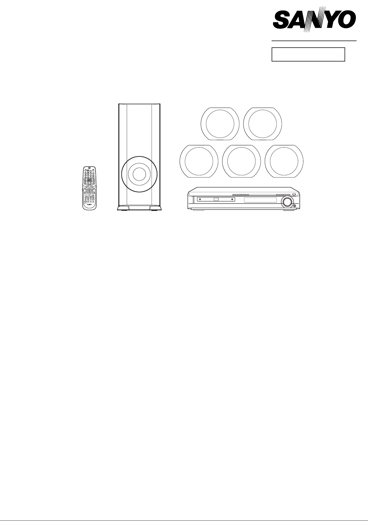
DVD Home Theater System
DC-TS760
(UK)
(XE)
PRODUCT CODE No.
129 656 03 UK
129 656 04 XE
Specification.......................................................................... 1
Laser beam safety precaution............................................... 2
Mechanism replacement ....................................................... 2
Trouble shooting ................................................................... 5
Service mode ........................................................................ 9
How to load software for MPEG P.W.Board ......................... 12
Tuner Adjustment.................................................................. 13
Exploded View (Cabinet & Chassis) ..................................... 14
Parts List ............................................................................... 15
Exploded View (DVD Mechanism) ........................................ 20
Parts List ............................................................................... 20
IC Block Diagram & Description............................................ 21
Block diagram ....................................................................... 36
Schematic Diagram (DVD).................................................... 38
Schematic Diagram (MPEG)................................................ 40
Schematic Diagram (AMP ).................................................. 42
Wiring Diagram (MAIN A side) ........................................... 44
(MAIN A side Top Left) ...................................................... 46
(MAIN A side Bottom Left) ................................................. 48
(MAIN A side Top Right) .................................................... 50
(MAIN A side Bottom Right) ............................................... 52
(B side)............................................................................... 54
Schematic Diagram (FRONT , TUNER)............................... 56
Wiring Diagram (FRONT , SW1 BUTTON, SW2 BUTTON,
MECHA SW and MECHA IF) ............................................ 58
Wiring Diagram (TUNER and COMPONENT) ................... 60
Wiring Diagram (POWER SUPPLY) .................................. 62
Wiring Connection................................................................ rear
REFERENCE No.
SM5810382
Page 2

SPECIFICATIONS
Amplifier
Main amplifier
Stereo mode
33 W x 2 (at 8 ohms, 10% distortion)
Dolby Digital mode
33 W x 2 (at 8 ohms, 10% distortion, with Centre/Surround/
Subwoofer amplifier off)
Centre amplifier
33 W (at 8 ohms, 10% distortion, with Main/Surround/Subwoofer
amplifier off)
Surround amplifier
33 W x 2 (at 8 ohms, 10% distortion, with Main/Centre/Subwoofer
amplifier off)
Subwoofer amplifier
55 W (at 4 ohms, 10% distortion, with Main/Centre/Surround
amplifier off)
Input:
VIDEO (AUDIO) IN: 500 mV/50 kΩ
Input/Output:
AV EURO/TV (AUDIO) IN (RGB OUT): For Euro-AV/Scart lead
Outputs:
SPEAKERS:
FRONT (L/R): 8 Ω
CENTER: 8 Ω
SURROUND (L/R): 8 Ω
SUBWOOFER: 4 Ω
MONITOR OUT:
S-VIDEO:
Y: 1.0 Vp-p (75 Ω)
C: 0.3 Vp-p (75 Ω) PAL, 0.286 Vp-p (75 Ω) NTSC
VIDEO: 1.0 Vp-p (75 Ω)
DVD Player
Type:
DVD video player
Playback standard:
PAL or NTSC
Laser:
Semiconductor laser, wavelength: 650/790 nm
Laser output (Continuous wave max.):
1 mW (DVD)
0.5 mW (CD)
Signal to noise ratio:
More than 105 dB
Wow and flutter:
Below measurable level
Tuner
Reception frequency:
FM: 87.5 - 108 MHz
AM: 522 - 1611 kHz
General
Power requirements:
AC 230 V, 50 Hz
Power consumption:
120 W
1.5 W (standby mode)
Dimensions:
435(W) x 65(H) x 378(D) mm
Weight:
5.6 kg
Speaker system
Front left, Front right, Centre, Surround left and Surround right
speakers (SX-TS760S, magnetic shield)
Unit used:
8 cm cone type, full range
Maximum power handling capacity:
50 W (peak)
Nominal impedance:
8 Ω
Dimensions:
125(W) x 105(H) x 112(D) mm
Weight:
0.72 kg/speaker
Subwoofer (SX-TS760W)
Unit used:
13 cm cone type
Maximum power handling capacity:
80 W (peak)
Nominal impedance:
4 Ω
Dimensions:
160(W) x 395(H) x 305(D) mm
Weight:
4.6 kg
IMPORTANT INFORMATION
Because its products are subject to continuous improvement, SANYO
reserves the right to modify product designs and specifications without
notice and without incurring any obligation.
- 1 -
Page 3
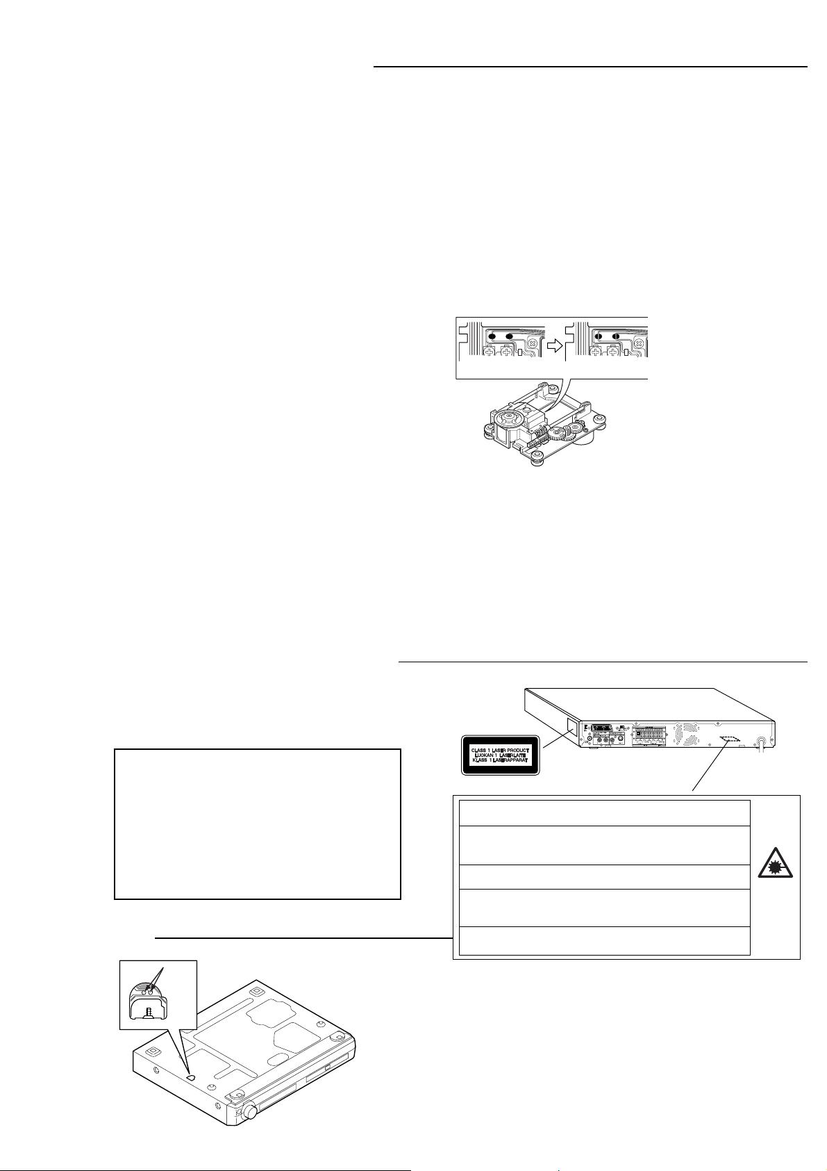
DVD MECHANISM REPLACEMENT
1. Cautionary instructions in handling the assy
(Safety instructions)
Optical pickup
The laser beam used in the pickup is classified as "class 2".
Exposing your eyes or skin to the beam is harmful. Take care
not to do so.
(Caution against static electricity and leakage voltage)
Ground securely the work tables, tools, fixtures, soldering irons
(including those made of ceramic) and measuring instruments
used in the production lines and inspection departments that
handle loaders. The workers shall also be grounded.
(Cautionary instructions in handling)
Do not touch the object lens when handling a loader, or the lens
will be stained, resulting in inadequate playability.
There is no power supply protection circuit provided for this
product or adjustment/inspection device. Short-circuiting may
lead to fire or damage.
Take care so as to protect from exposure to water, the entry of
metallic pieces or dew condensation.
In particular, a strong magnet adjacent to the pickup will not only
get inoperative but can damage the pickup if a small metallic
piece, such as a screw or swarm, enters.
The loader edge can cause injury if inadvertently handled.
Do not touch a rotating disk, or injury may result.
This product is a precision device. Handle carefully.
A shock or dropping will cause misalignment or destruction. If it
should occur, refer to clause 2.
This product is so designed as to endure an initial shock
equivalent to a drop from a height of approx. 90 cm under the
packed condition.
After the initial shock, the resistivity will still remain at a level of
50 to 60 G, but the mechanical robustness will weaken.
Do not place in a dusty location.
The entry and deposition of dirt into or on the pickup lens or
moving section will cause malfunction or degradation.
(Connectors)
Do not connect or disconnect while power is on.
Connecting or disconnecting signal wires or the main power cord
when the power is on may destruct the unit or fixture.
When connecting, push all the way in securely.
An insufficient insertion may cause a bad contact, leading to an
erroneous operation.
Do not connect or disconnect roughly by an excessively strong
force, or a broken wire or bad contact may result.
Semiconductors are connected. Do not touch connector terminals
directly.
If the worker is grounded, there is nothing to worry about static
electricity, but the rust on the connector terminal surface caused
by the touch may result in bad contact.
(Caution)
Before disconnecting FFC
cable, make it "SHORT" as
shown left.
After connecting FFC
cable,make it "OPEN" as
shownleft.
(OPEN)(SHORT)
(Power source)
The power source need be good in quality (free from instantaneous
interruptions or noises).
A low quality power source may well cause malfunction.
(Storage)
Do not place or store in a dusty place or a place where dew
condensation is possible.
The entry and deposition of dirt or dust into or on the pickup lens or
moving section will cause malfunction or degradation.
Also, dew condensation causes rust; the rust penetrate into the
precision part of a pickup, causing malfunction, or degrading the
optical quality of the internal lens and reflector, which also leads to
malfunction.
LASER BEAM SAFETY PRECAUTION
• Pick-up that emits a laser beam is used in this CD player section.
CAUTION :
USE OF CONTROLS OR ADJUSTMENTS
OR PERFORMANCE OF PROCEDURES
OTHER THAN THOSE SPECIFIED HEREIN
MAY RESULT IN HAZARDOUS RADIATION
EXPOSURE
LASER OUTPUT.......... 0.6 mW Max. (CW)
WAVELENGTH ............. 790 nm
RESET
Short
It is reset by short.
CAUTION – INVISIBLE LASER RADIATION WHEN OPEN AND
INTERLOCKS DEFEATED. AVOID EXPOSURE TO BEAM.
ADVARSEL – USYNLIG LASER STRÅLING VED ÅBNING, NÅR
SIKKERHEDSAFBRYDERE ER UDE AF FUNKTION, UNDGÅ UDS ÆTTELSE
FOR STRÅLING.
VARNING – OSYNLIG LASER STRÅLNING NÄR DENNA DEL ÄR ÖPPNAD
OCH SPÄRR ÄR URKOPPLAD. STRÅLEN ÄR FARLIG.
VORSICHT – UNSICHTBARE LASERSTRAHLUNG TRITT AUS, WENN
DECKEL GEÖFFNET UND WENN SICHERHEITSVERRIEGELUNG
ÜBERBRÜCKT IST. NICHT, DEM STRAHL AUSSETZEN.
VARO – AVATTAESSA JA SUOJALUKITUS OHITETTAESSA OLET ALTTIINA
NÄKYMÄTTÖMÄLLE LASERSÄTEILYLLE. ÄLÄ KATSO SÄTEESEEN.
- 2 -
Page 4
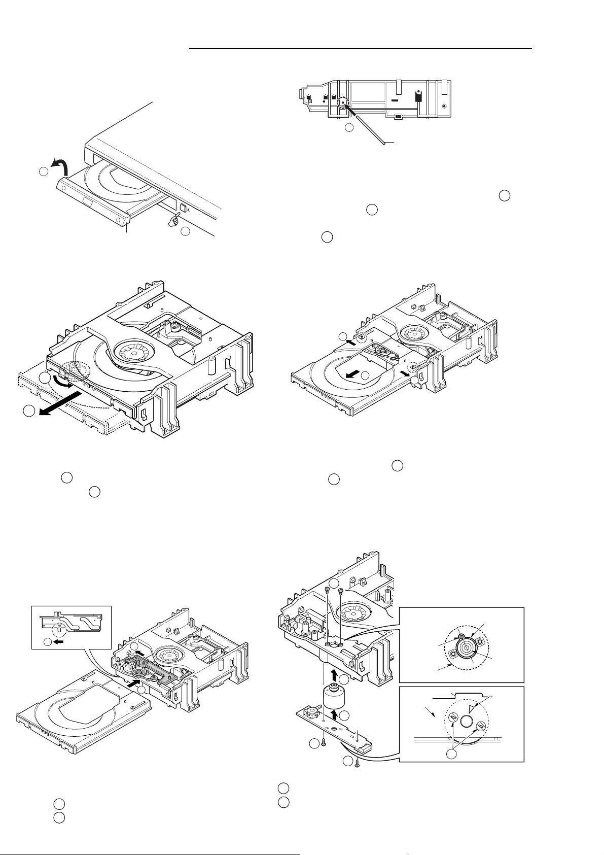
MECHANISM REPLACEMENT
1. How to Remove DVD Mechanism
First, it is necessary to remove Escutcheon.
1
2
Escutcheon
1
2. How to remove the tray.
Side of DVD mechanism
Front
3
Cylindrical thing
Rear
How to remove Escutcheon.
1
An eject button is pushed and a tray is taken out.
Please remove Escutcheon, as shown in the left figure 2 .
When an eject button 1 does not function. Above figure
Please insert a cylindrical thing with a diameter of 3mm or less
in the hole 3 in the side of a DVD mechanism.
A tray is pushed out.
1
1
2
Rotate the 1 gear.
Move forward the 2 tray.
3. How to insert the tray.
1
2
1
Move both the right and left 1 tray pins to the ends.
Remove the 2 tray.
4. How to install the motor.
2
SHASSIS
HOLE
1
1
2
3
ROUND
HOLE
MOTOR
MECHA
P. W. B
PULLEY
TRIANGLE
MARK
Move the 1 slide to the left end.
Insert the 2 tray.
4
4
SOLDERING
5
1 Adjust the motor terminal to boss in the chassis.
2 Adjust the round hole of the motor to the triangle mark of
P.W.B,and solder it.
- 3 -
Page 5
MECHANISM REPLACEMENT
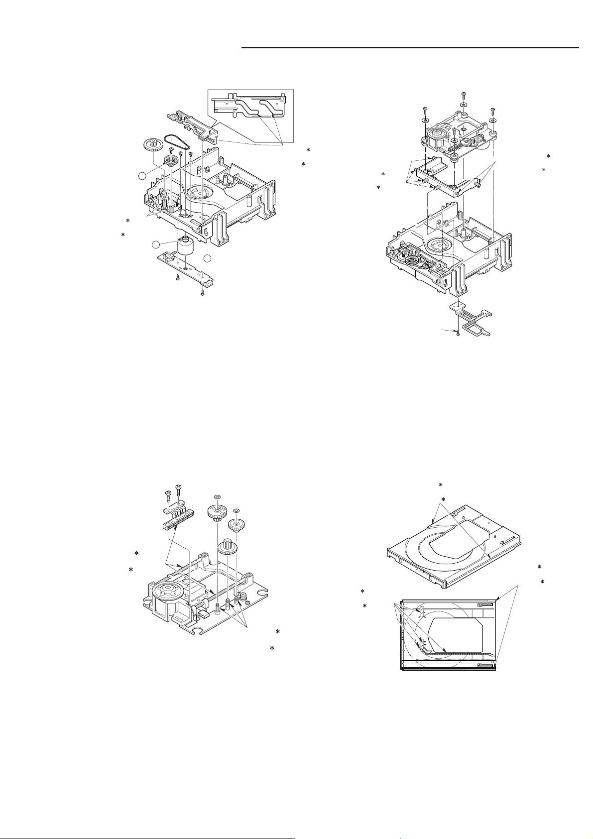
5. Base mechanism mounting parts.
A
G-FLOIL GREASE SY-31S
G-FLOIL GREASE MEN-223R
or
G-FLOIL GREASE SY-31S
G-FLOIL GREASE MEN-223R
A
A
: Clean the groove by alcohol well.
or
G-FLOIL GREASE SY-31S
G-FLOIL GREASE MEN-223R
or
Apply screw lock
G-FLOIL GREASE SY-31S
G-FLOIL GREASE MEN-223R
or
6. Base mechanism parts.
G-FLOIL GREASE SY-31S
or
G-FLOIL GREASE MEN-223R
G-FLOIL GREASE SY-31S
or
G-FLOIL GREASE MEN-223R
Do not remove the pick-up from base mechanism because of
adjustment difficulty.
7. Tray parts.
G-SANKOL CFD-409Z
or
G-HANARL SF-106B
G-SANKOL CFD-409Z
or
G-HANARL SF-106B
G-SANKOL CFD-409Z
or
G-HANARL SF-106B
- 4 -
Page 6
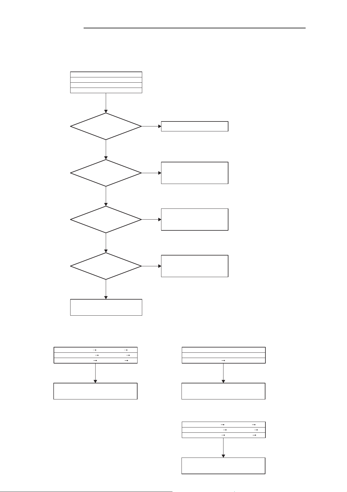
TROUBLE SHOOTING
VIDEO COMPOSITE OUT ; OK
TUNER OUTPUT ; OK
VIDEO 1,2 OUTPUT ; OK
DVD/CD OUTPUT ; NG
LOADER CHANGE
OK?
N
3.3V,DAC5V
CONFIRM
CN870 Pin1,15,18
Y
IC870 Pin17,19,21,23,25,27
CONFIRM
Y
IC800 AMCLK,ALRCLK,
AOUT0~2,ML,MC,MD1 CONFIRM
Pin2~7,12~14,47
N
Y
N
N
Y
LOADER CHANGE
DAC5V LINE CONFIRM
3.3V LINE CONFIRM
IC412 PERIPHERAL CIRCUIT
CONFIRM (IC411,IC410 etc)
DAC IC870 PERIPHFRAL CONFIRM
DAC IC870 NG
MUTE CIRCUIT
Q8880 PERIPHERAL CIRCUIT
DAC IC870 NG
CONFIRM
IC820 Pin
FLOATING CONFIRM
IC820 NG
TUNER OUTPUT ; L,R OK / C,SL,SR,SW NG
VIDEO 1,2 OUTPUT ; L,R OK / C,SL,SR,SW NG
DVD/CD OUTPUT ; L,R OK / C,SL,SR,SW NG
C,SL,SR,SW PERIPHERAL CONFIRM
(IC451,471,472,482,483,452,450,491
PERIPHERAL CONFIRM)
TUNER OUTPUT ; NG
VIDEO 1,2 OUTPUT ; OK
DVD/CD OUTPUT ; OK
IC460,451 CONFIRM
TUNER OUTPUT ; L,R OK / C,SL,SR,SW NG
VIDEO 1,2 OUTPUT ; L,R OK / C,SL,SR,SW NG
DVD/CD OUTPUT ; L,R OK / C,SL,SR,SW OK
Q SURROUND , Volume CONFIRM
(IC452,451 PERIPHERAL CONFIRM)
- 5 -
Page 7
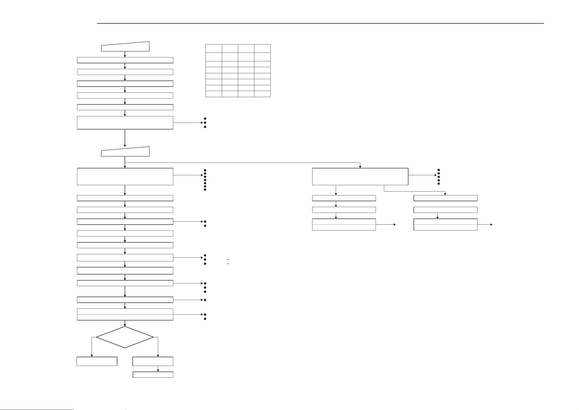
TROUBLE SHOOTING
AC CORD PLUG
IC430,IC601 +5V POWER ONLY
IC430 RESET
X4300 CLOCK
IC430 ACTIVE
IC601 COMMUNICATION
POWER SUPPLY ; STANDBY mode
IC430 ACTIVE / P-CON ; LOW
±12V,±7V,DVD-POWER ; OFF / FIL,-30V ; ON
POWER KEY PRESS
DVD FUNCTION
P-COM ; HIGH
DVD-POWER ; HIGH
IC430 STANDBY DATA WAIT
±12V,±7V ; ON
IC451,IC452 COMMUNICATION
IC430
X4300
IC451
IC601
IC870
IC801
IC410
IC411
NG
FM,AM,VIDEO1,VIDEO2 (VIDEO,TV)
NG
IC430 VDD,RESET,OSC CONFIRM
IC430 COMMUNICATION CONFIRM
P-CON,FIL,-30V CONFIRM
POWER KEY CONFIRM
IC601 COMMUNICATION CONFIRM
PROTECT CIRCUIT CONFIRM
IC462,IC472,IC482,IC483 CONFIRM
P-CON
±12V,±7V,P-CON CONFIRM
DVD-POWER CONFIRM (IC410,IC411 etc)
SYSCON
SYS-CLK
FUNCTION
&
VOLUME
VFD-DRV
6CH-DAC
EEPROM
REG.
REG.
IC241
DS601
IC800
IC818
IC821
IC822
TU-PLL
IR
DVD-MPU
&
MPEG
FLASH
SDROM
SDRAM
P-COM ; HIGH /
DVD-POWER ; LOW
IC430 STANDBY DATA WAIT
±12V,±7V ; ON
IC451,IC452 COMMUNICATION
NG
IC451,IC452,IC241 COMMUNICATION
POWER KEY CONFIRM
IC601 COMMUNICATION CONFIRM
PROTECT CIRCUIT CONFIRM
IC462,IC472,IC482,IC483 CONFIRM
±12V,±7V,P-CON CONFIRM
TUNERVIDEO1, VIDEO2 (VIDEO,TV)
INITIALIZE ADAC (IC870)
RESET LOADER
READ,WRITE DATA IN EEPROM (IC801)
IC800 START COMMUNICATION WITH IC430
FROM MPU STANDBY DATA SEND
IC430 STANDBY DATA RCVD
IC430 VFD DATA RCVD
IC430 VFD DATA SEND
IC601 VFD DATA RCVD
DISPLAY OPENNING
START CONTROL OF LOADER
PICK INITIALIZE SPINDLE ROTATE
DISC Y/N
NY
NG
NG
NG
NG
NG
VDD,CLOCK CONFIRM
IC800 PERIPHERAL CIRCUIT CONFIRM
COMMUNICATION LINE CONFIRM
REMOCON NG IC430 & DS601 PERIPHERAL CONFIRM
REMOCON OK IC430 PERIPHERAL CONFIRM
*1
IC601 & IC430 PERIPHERAL CONFIRM
-30V FILAMENT VOLTAGE CONFIRM
COMMUNICATION LINE CONFIRM
IC800,IC818,IC822 BUS-LINE CONFIRM
LOADER CONFIRM
COMMUNICATION LINE CONFIRM (FFC)
IC430 VFD DATA SEND
IC601 VFD DATA RCVD
VFD INDICATE "VIDEO1" or "VIDEO2"
IC430 VFD DATA SEND
NG
*1 *1
IC601 VFD DATA RCVD
VFD INDICATE "FM" or "AM"____k(M)Hz
NG
IVFD INDICATE
"NO DISC"
VFD INDICATE
"READING"
PLAYBACK MODE
- 6 -
- 7 -
Page 8
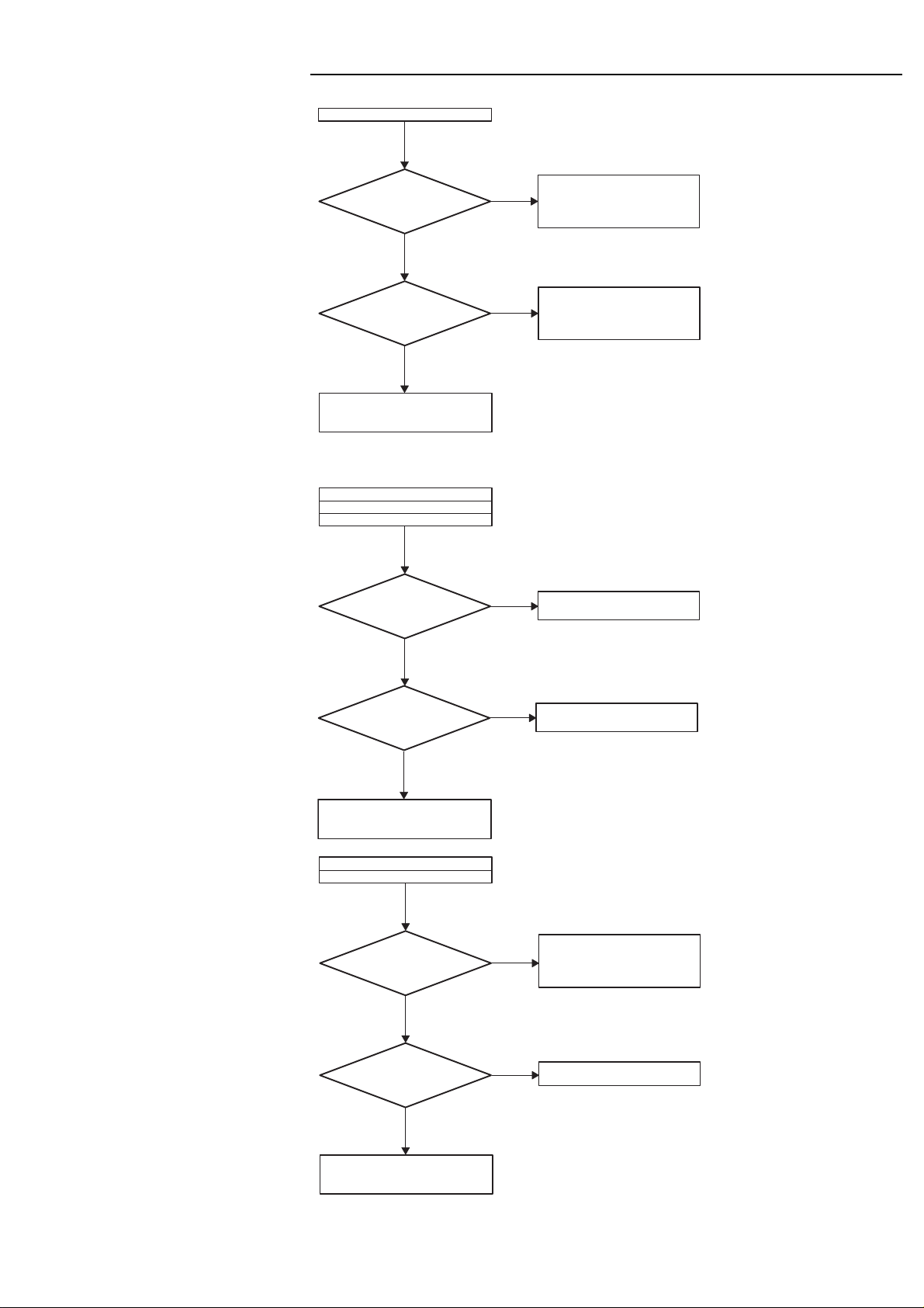
TROUBLE SHOOTING
NO COLOR or ABNORMAL
X8230
27MHz
OK?
Y
IC800
VIDEO OUTPUT
NORMAL OK?
N
IC800 NG
FLOATING CONFIRM
IC800 NG
TUNER OUTPUT ; NG
VIDEO 1,2 OUTPUT ; OK
DVD/CD OUTPUT ; OK
CN241 Pin10,11
5.6V,12V OK?
N
Y
N
CRYSTAL RESONATOR
CHANGE
IC800 OUTPUT LINE CONFIRM
Pin 169~173 PERIPHERAL
CONFIRM
LPF CONFIRM
IC402,IC401 PERIPHERAL
CONFIRM
Y
IC211,IC231,IC241,(IC251)
PERIPHERAL CONFIRM
N
IC460,IC451 PERIPHERAL CONFIRM
NO PICTURE
AUDIO OK
IC800
VIDEO OUTPUT
NORMAL OK?
N
LOADER CHANGE
OK?
N
Y
Y
IC211,231,IC241(IC251) NG
IC800 OUTPUT LINE CONFIRM
Pin169~173
CONFIRM
LPF CONFIRM
LOADER CHANGE
N
IC800 Pin
FLOATING CONFIRM
IC800 NG
- 8 -
Page 9
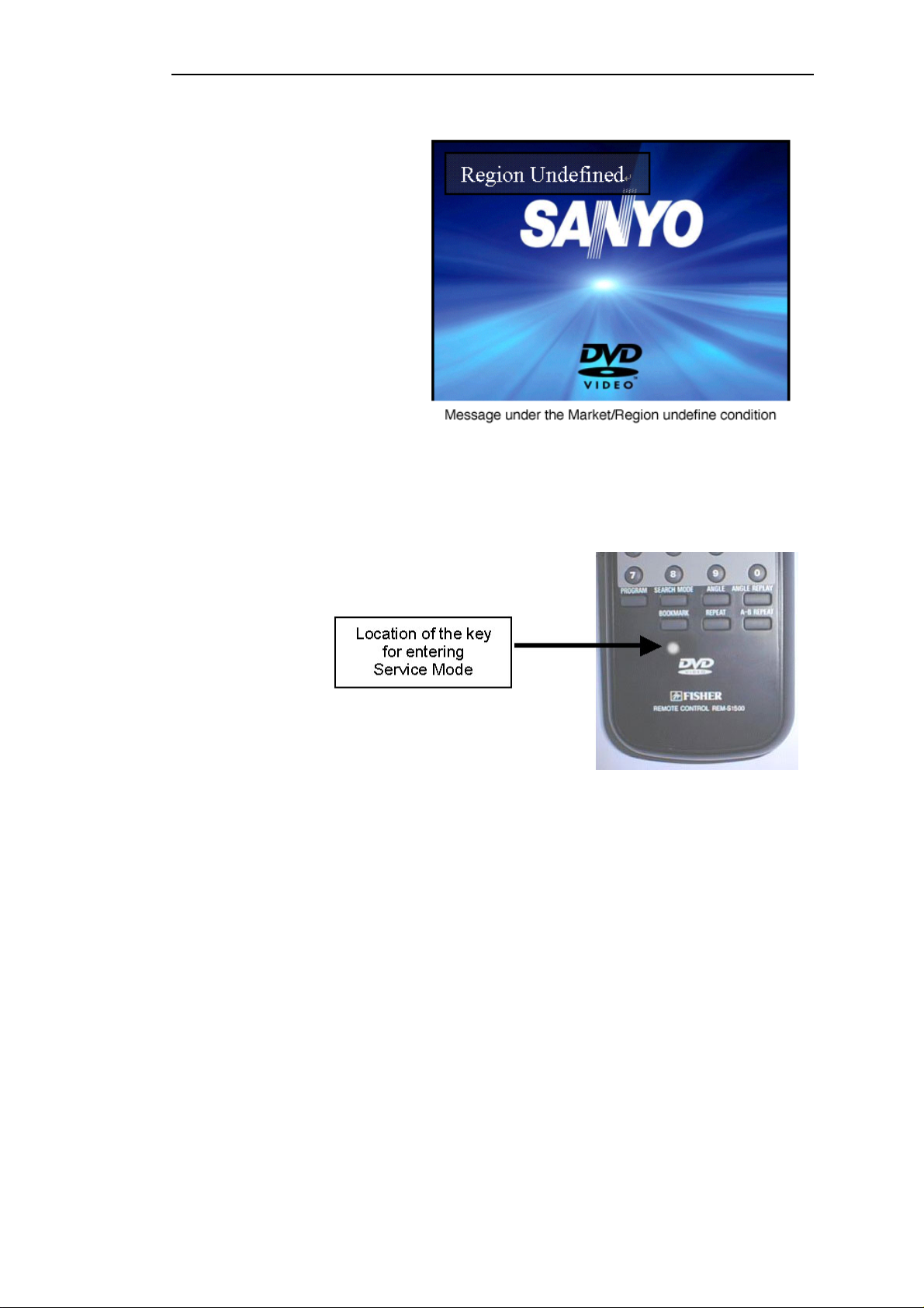
SERVICE MODE
A. Market / Region SETUP
In the initial condition for this model, Market and Region
information are undefined.
In the following cases, be sure to set up Market/Region.
1. When updating the system using CD-R
(Part code : 0PRADF9655--AA).
2. When replacing a DVD substrate.
While Market/Region information are undefined, the message
"Region Undefined" is displayed on the screen.
NOTE: Even if the condition is not under 1 or 2 above, if the
message "Region Undefined" is displayed, be sure to set up
Market/Region.
B. How to enter Service Mode.
You can enter Service Mode in any one of the following ways (1 to 3).
1. Pushing the covered key located beneath Book Mark key on RB 1500 or REM-S1500.
2. Simultaneously pushing both Shift key and ON SCREEN key on
REM-TS760MT(US),RB-TS760MT(CA) or RB-TS760ST(UK,XE).
- 9 -
Page 10
SERVICE MODE
C. Setup Procedures
1. Displaying SERVICE MODE screen
Display Service Mode screen following the instructions "How to
enter Service Mode" above.
2. Displaying Internal Setup screen
Push NEXT button within three seconds after operating the
Service Mode display.
On the Internal Setup screen shown on the right, set up Market
and Region.
Region
BackendVersion
LoaderVersion
0
Market
S21225A1
55 50 05
Internal Setup
Markett W M
00
Region 1
WM
Value
Model Market Region
DC-760/UK UK 2
DC-760/XE XE 2
Market/Region setup table.
3. Setting Market code
3.1. While a highlighted indicator is displayed on the right side
of the Market denotation, push ENT button on the remote
controller.
With each push the indicator will advance as shown
below.
3.2. Specify the code of the model in accordance with the
Market/Region Setup Table above.
3.3 Once the desired code is displayed, push p button to
move the highlighted indicator to the Region input area.
00-WM
01-SFC
S18
05-SS 06-PA
02-UK
07-AU 08-CN
Internal Setup
Markett W M
00
Region 1
00-WM
01-SFC
S18
05-SS 06-PA
02-UK
07-AU 08-CN
03-XE
03-XE
Exit
09-JP
Exit
09-JP
04-
04-
- 10 -
(Reference figure)
Page 11

SERVICE MODE
4. Setting REGION code
4.1 While a highlighted indicator is displayed on the right side
of the Region denotation, push ENT button on the remote
controller. With each push the indicator will advance as
shown below.
1 -> 2 -> 3 -> 4 -> 5 -> 6
Internal Setup
Market
Region
00
1
1
Exit
4.2 Specify the number of the model in accordance with the
Market/Region Setup Table above.
4.3 Once the desired number is displayed, push p button to
move the highlighted indicator to Exit area.
5. Saving settings
5.1 Make sure that the Market and Region settings are properly
set.
(If any of the settings are incorrect, you can make a change
by moving the indicator using p button, and following
procedures 3 and 4 above. )
5.2 After ensuring that the settings are all correct, push ENT
button while the indicator is on Exit area. The settings are
now saved.
00-WM
01-SFC
02-UK
S18
05-SS 06-PA
07-AU 08-CN
Internal Setup
Market
Region
00-WM
01-SFC
S18
05-SS 06-PA
02-UK
07-AU 08-CN
00
1
03-XE
04-
09-JP
(Reference figure)
Exit
03-XE
04-
09-JP
6. Finishing settings
6.1 After a few seconds, the Internal Setup screen disappears,
and then the Service Mode screen is displayed again for
three seconds as shown on the right.
You should check the settings.
Backend version
Brand (S : SANYO , F : FISHER)
Version ( 2 0 0 2 , 12 , 25)
Sub Version (A,B,......Z)
Region ( 0 : Region undefined
1 ~ 6 : Region defined )
6.2 Power OFF.
S 21225 A 1
- 11 -
Region
BackendVersion
LoaderVersion
1
Market
S21225A1
55 50 05
(Reference figure)
WM
Value
(Reference figure)
Page 12

SERVICE MODE
D. IMPORTANT NOTE
1. Once the "Market/Region" settings are written into EEPROM (IC818) on the DVD substrate, they cannot be reset.
(However, updating the system using CD-R enables you to make new settings.)
2. While the Internal Setup screen is displayed, pushing the Power button enables you to terminate the operations without
making any settings.
HOW TO LOAD SOFTWARE FOR MPEG P.W.BOARD
1. Power on, then open tray.
2. It take on CD-ROM for UPDATE software to the tray, and tray close.
3. Display " READING " in the TV screen.
4. For the time being, tray open and FL display remain "UP DATING".
5. When software loading finished, FL display "GOODBY".
6. Next, set up market code and region code by "SERVICE MODE"
CD-ROM part code is "0PRADF9655--AA".
CAUTION
After an MAIN board(614 326 0172) or IC ASSY(410 469 7906) exchange should carry out loading of the software by the
newest CD-R, and should check operation.
- 12 -
Page 13
TUNER ADJUSTMENTS
J2003
1
1
0
J2007
J
J2005
200
J
2102
04
211
01
1
J
2
J20
13
2201
22
J2064
J
J2061
J
J2261
J
J2
J
1
3
3
02
32
5
1
13C
0
J2121
J2
2
J2024
J
2
J
02
901
22
J2025
J
J2142J2J14
J2143JJ2
J2144
J214
J2
04
245
2
4C14C
2
J2141
J214
J214
J214
J2041
J204
2
4
J2044
J
J2048
J
242
51
C2
2153
C
C2123CC
C2C
0
0
10
02
10
21
07
C
03
2
6
C2
C
3
30
23
2
C
0303
6
6
1
C2314
C
C
4
C246
C
624C
4
C
• Use a plastic screw driver for adjustments.
SG RF Level : 75Ω open Voltage dBµV
Antenna : 75Ω unbalanced Direct, Modulation : 1 kHz
Dev. : ±22.5kHz(MONO) , ±22.5kHz(STEREO) , ±6.75kHz(PILOT)
Output Level : about 100mV at TP13,TP14,TP15
L2101
J2203
J2008
TP12
(GND)
L215
L2151
L2102
J2009
TP11 TP12
J2229
C2113
TP25
XF222
TP24
J2027
XF231
XF231
1.FM
---
---
Connection
Connect Digital DC voltmeter
to TP11(H), TP12(E).
IC231 3,22pin
TP24, TP25
Step Adjusting
Circuit
1 IF Alignment
2 Cover
voltage
3 Tracking Connect FM SG to FM Antenna Connect to VTVM
Input Output
FM ANT.
SG=66dBµV
(SG= about 8dBµV) TP13(L) or TP14(R), TP15(E)
IC231
XF233
TP15 TP13
2
21
R2311
R2301
C2327
SG Set Adjustment Remark
Frequency Position
J2161
TP14
D2451
J2062
98.0MHz --- XF233 0.0 ± 0.05V
87.5MHz Low
108.0MHz High
90.0MHz Low
L2102
L2101 Max.
Alignment voltage is
more than 0.8V.
Confirm voltage is less
than 9.0V.
106.0MHz High
NC
RDS
TU-CLK
TU-L
TU-R
5.6V
+12V
TU-CE
TU-DO
A-GND
TU-DATA
1AD4B10D1740B
T002 94V-0
2.AM
---
---
Connection
IC231 19pin(DCCUT)
Connect Digital DC voltmeter
toTP11(H), TP12(E).
TP13(L) or TP14(R), TP15(E).
TP26(GND)
Step Adjusting
Circuit
IF Alignment Loop Ant.
1
2 Cover
voltage
3 Tracking Connect AM SG to Connect to VTVM
Input Output
Test loop Ant.
(SG= About 80dBµV)
SG Set Adjustment Remark
Frequency Position
522kHz XF231
522kHz Low --- more than 0.8V
1611 kHz High --- less than 9.0V
603kHz Low
L2151-a Max.
1404kHz High
- 13 -
Page 14
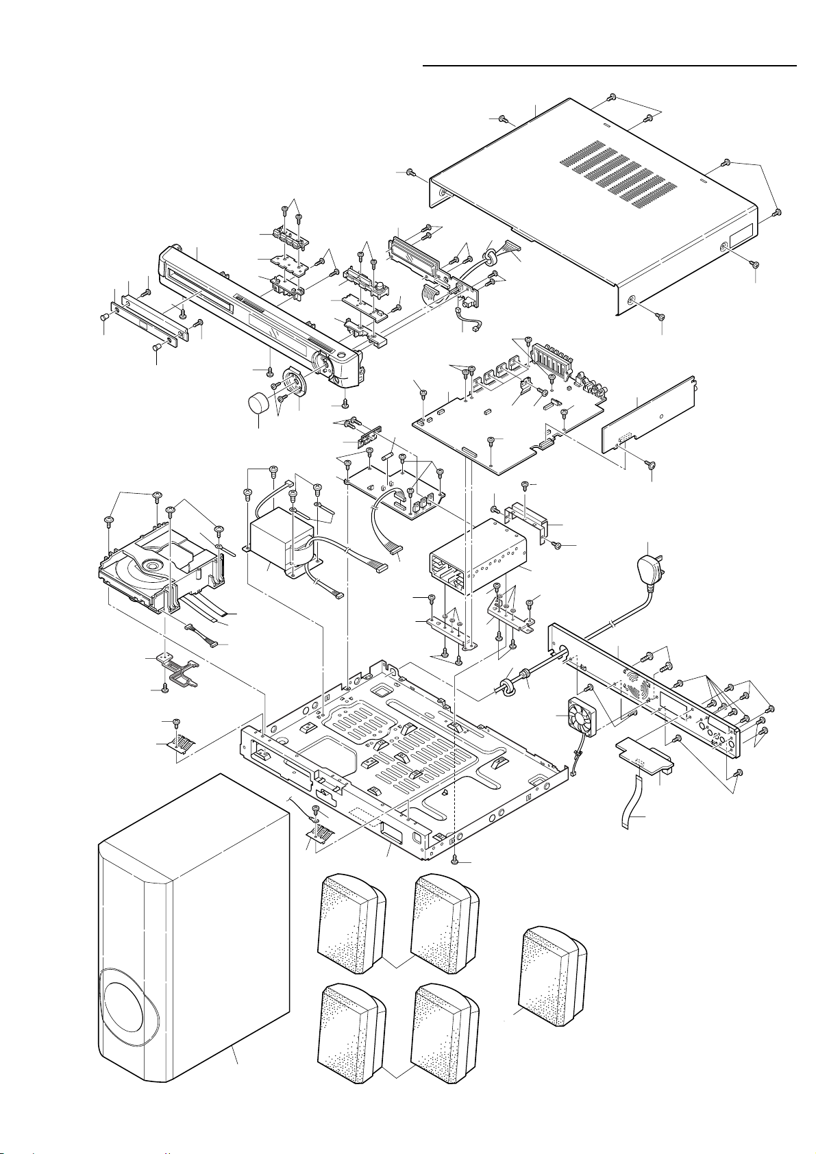
EXPLODED VIEW (CABINET & CHASSIS)
1
2
2
3
4
Y02
Y03
Y04
Y04
Y02
Y01
Y01
Y01
5
6
12
13
7
8
9
10
11
Y05
Y05
Y06
Y06
Y06
Y08
Y08
Y08
Y08
Y08
Y09
Y10
Y11
Y12
Y12
Y13
Y13
Y14
Y14
Y15
Y15
Y22
Y26
Y23
Y26
Y25
Y26
Y16
Y16
Y17
Y17
Y19
Y20
Y20
Y18
Y18
Y07
Y07
Y07
Y07
Y07
Y07
14
15
16
17
18
19
19
20
23
24
24
21
22
59
61
60
71
72
73
74
75
76
77
51
52
53
54
55
56
57
58
Y27
Y27
Y14
24
63
62
Y15
Y13
- 14 -
Page 15

PARTS LIST
PRODUCT SAFETY NOTICE
EACH PRECAUTION IN THIS MANUAL SHOULD BE FOLLOWED DURING SERVICING. COMPONENTS IDENTIFIED WITH THE
!!
IEC SYMBOL
PERFORMANCE CAN BE OF SPECIAL SIGNIFICANCE. WHEN REPLACING A COMPONENT IDENTIFIED BY
REPLACEMENT PARTS DESIGNATED, OR PARTS WITH THE SAME RATINGS OF RESISTANCE, WATTAGE OR VOLTAGE THAT
ARE DESIGNATED IN THE PARTS LIST IN THIS MANUAL. LEAKAGE-CURRENT OR RESISTANCE MEASUREMENTS MUST BE
MADE TO DETERMINE THAT EXPOSED PARTS ARE ACCEPTABLY INSULATED FROM THE SUPPLY CIRCUIT BEFORE
RETURNING THE PRODUCT TO THE CUSTOMER.
CAUTION : Regular type resistors and capacitors are not listed. To know those values, refer to the schematic diagram.
PACKING & ACCESSORIES
REF.NO. PART NO. DESCRIPTION
or 614 308 5515 ANT,FM ANT
or 645 043 9735 BATTERY COVER,SERVICE PART
23 614 326 6563 ASSY,BOX,SPEAKER,
23 614 326 6570 ASSY,BOX,SPEAKER,
24 614 326 6549 ASSY,BOX,SPEAKER,
24 614 326 6556 ASSY,BOX,SPEAKER,
CABINET & CHASSIS
REF.NO. PART NO. DESCRIPTION
1 614 326 0271 ASSY,CABINET,FRONT
2 614 325 8223 CAP,DVD TRAY
3 614 327 1710 ASSY,DEC,
3 614 326 3517 ASSY,DEC,
4 614 325 5680 DEC,DVD TRAY
5 614 322 4839 KNOB,ROTARY,VOLUME
6 614 325 5703 DEC,ESCUTCHEON VOL
7 614 325 5628 BUTTON,FUNCTION,FUNCTION
8 614 325 5765 MOUNTING,BUTTON FUNCTION
9 614 325 5611 BUTTON,POWER,POWER /PLAY
10 614 325 5758 MOUNTING,BUTTON POWER
11 614 325 5635 CABINET,TOP/SIDE
12 614 316 1417 MOUNTING,IC,IC-HEAT SINK
13 614 291 6568 MOUNTING,PWB,IC-HEAT SINK
14 614 325 5666 COVER,FAN
or 645 001 0415 T-VINYL*223S,FAN COVER
15 614 325 5727 HEAT SINK
16 614 322 4815 HOLDER,REAR,HEAT SINK
17 614 322 4822 HOLDER,BOTTOM,HEAT SINK
18 614 322 5997 MOUNTING,FFC,MOUNTING
or 614 320 5852 MOUNTING,FFC,MOUNTING
!
IN THE PARTS LIST AND THE SCHEMATIC DIAGRAM DESIGNATED COMPONENTS IN WHICH SAFETY AND
!!
!
, USE ONLY THE
Regular type resistors are less than 1/4 W carbon type and chip resistors.
Regular type capacitors are less than 50 V and less than 1000 µF type of Ceramic type and Electrical type.
REF.NO. PART NO. DESCRIPTION
19 614 313 6545 SPRING,PLATE,EARTH
645 020 7020 ASSY,ANTENA,LOOP
645 041 1373 CABLE,VIDEO
614 326 6754 CARTON CASE,INNER(UK)
614 326 6761 CARTON CASE,INNER(XE)
614 325 9237 CUSHION,LEFT
614 325 9244 CUSHION,RIGHT
614 326 6778 INSTRUCTION MANUAL(UK)
614 326 6785 INSTRUCTION MANUAL(XE)
614 326 6792 INSTRUCTION MANUAL,GREEK(XE)
645 052 1621 POLY BAG,VIDEO/AUDIO(UK)
645 048 2182 POLY BAG,VIDEO/AUDIO(XE)
645 052 1416 POLY BAG,AC CORD(UK)
645 012 2958 POLY BAG,INST MANUAL(UK)
645 013 6535 POLY BAG,INST MANUAL(XE)
645 048 1994 POLY SHEET,SET(UK)
645 045 3540 POLY SHEET,SET(XE)
645 058 1113 REMOCON,RB-TS760ST
614 229 4635 ANT,FM ANT
645 048 5053 BATTERY COVER,BATTERY COVER
SUB WOOFER,SX-TS760W/UK(UK)
SUB WOOFER,SX-TS760W/XE(XE)
SATELLITE,SX-TS760S/UK(UK)
SATELLITE,SX-TS760S/XE(XE)
ESCUTCHEON TRAY(UK)
ESCUTCHEON TRAY(XE)
20 614 325 5604 ASSY,CABINET,BOTTOM
21 614 129 1901 FIXER,AC CORD
or 614 284 1884 FIXER,AC CORD
or 614 129 4971 FIXER,AC CORD
22 614 326 0349 PANEL,REAR,INT(UK)
22 614 326 3913 PANEL,REAR,INT(XE)
FIXING PARTS
REF.NO. PART NO. DESCRIPTION
Y01 411 021 6405 SCR S-TPG BIN 3X8,
CABINET FRONT-BOTTOM
Y02 411 098 4700 SCR S-TPG BIN 2.3X8,
DEC ESC-TRAY
Y03 411 098 4700 SCR S-TPG BIN 2.3X8,
CABINET FRONT-ESC VOL
Y04 411 098 4700 SCR S-TPG BIN 2.3X8,
PWB-BUTTON FUNCTION
Y05 411 098 4700 SCR S-TPG BIN 2.3X8,
PWB-BUTTON POWER
Y06 411 098 4700 SCR S-TPG BIN 2.3X8,
CABINET FRONT-PWB FIX
Y07 411 098 4205 SCR S-TPG BIN 3X8,CABINET
Y08 411 021 6405 SCR S-TPG BIN 3X8,MAIN PWB
Y09 411 021 6405 SCR S-TPG BIN 3X8,
HOLDER H/S-HEAT SINK
Y10 411 020 9902 SCR S-TPG BRZ+FLG 3X8,
TUN PWB
Y11 411 021 6405 SCR S-TPG BIN 3X8,
HOLDER H/S-PWB
Y12 411 021 6405 SCR S-TPG BIN 3X8,POWER PWB
Y13 411 021 6405 SCR S-TPG BIN 3X8,
COVER FAN-HEAT SINK
Y14 411 021 6405 SCR S-TPG BIN 3X8,
HOLDER H/S-BOTTOM
Y15 411 021 6405 SCR S-TPG BIN 3X8,
HOLDER H/S-BOTTOM
Y16 411 001 3905 SCR S-TPG BIN 4X6,PT
Y17 614 130 0382 LUG,LEAD TREATMENT
Y18 411 020 9803 SCR S-TPG BRZ+FLG 3X6,
DVD MECHA
Y19 411 021 2704 SCR S-TPG BIN 2.6X6,MOUNTING
Y20 411 021 6405 SCR S-TPG BIN 3X8,
EARTH SPRING PLATE
Y22 411 021 3701 SCR S-TPG BIN 3X10,
REAR-VIDEO OUT PWB
Y23 411 182 7501 SCR S-TPG BIN 5X16,
FAN-PANEL REAR
Y25 411 021 3701 SCR S-TPG BIN 3X10,
BOTTOM-REAR
Y26 411 021 3701 SCR S-TPG BIN 3X10,
REAR-ELECT PART
Y27 412 011 5903 SPECIAL WASHER,
HOLDER HEAT SINK
- 15 -
Page 16

PARTS LIST
ELECTRICAL-PARTS
REF.NO. PART NO. DESCRIPTION
51 614 325 7721 ASSY,WIRE,FRONT_SW1
52 614 325 7714 ASSY,WIRE,MAIN_FRONT
53 423 028 8405 FUSE 250V 1.6A
54 614 325 7707 ASSY,WIRE,MAIN_DG
55 645 057 9103 TRANS,POWER
56 645 058 3445 FLEXIBLE FLAT CABLE,PICK-FFC
or 645 053 8384 FLEXIBLE FLAT CABLE,PICK-FFC
57 645 058 3452 FLEXIBLE FLAT CABLE,IF-FFC
or 645 056 3010 FLEXIBLE FLAT CABLE,IF-FFC
58 614 323 3237 ASSY,WIRE,LOADING-DVD
59 645 054 0233 CORD,POWER-1.6MK(UK)
or 645 036 9797 CORD,POWER-1.6MK(UK)
or 645 036 9803 CORD,POWER-1.6MK(UK)
59 645 016 9939 CORD,POWER-1.74MK,FOR XE(XE)
or 614 255 2513 POWER CORD,FOR XE(XE)
60 645 058 3476 FLEXIBLE FLAT CABLE,
MAIN-SCART
or 645 054 3159 FLEXIBLE FLAT CABLE,
MAIN-SCART
61 645 053 3853 MOTOR,FAN DC 0.84W,FAN
62 645 051 0656 CORE,FERRITE
or 645 042 8999 CORE,FERRITE
63 645 051 0649 CORE,FERRITE
or 645 031 7637 CORE,FERRITE
SW2,BUTTON P.W.BOARD ASSY
REF.NO. PART NO. DESCRIPTION
71 614 325 6205 ASSY,PWB,SW2,BUTTON
(Only initial)
C6201 403 157 3601 CERAMIC 100P J 50V
CN621 614 035 4911 SOCKET,DIP 2P
S6201 645 037 2759 SWITCH,PUSH
or 645 006 5958 SWITCH,PUSH 1P-1T
or 614 220 5471 SWITCH,TACT
or 614 240 1002 SWITCH,TACT
S6202 645 037 2759 SWITCH,PUSH
or 645 006 5958 SWITCH,PUSH 1P-1T
or 614 220 5471 SWITCH,TACT
or 614 240 1002 SWITCH,TACT
S6203 645 037 2759 SWITCH,PUSH
or 645 006 5958 SWITCH,PUSH 1P-1T
or 614 220 5471 SWITCH,TACT
or 614 240 1002 SWITCH,TACT
S6204 645 037 2759 SWITCH,PUSH
or 645 006 5958 SWITCH,PUSH 1P-1T
or 614 220 5471 SWITCH,TACT
or 614 240 1002 SWITCH,TACT
SW1,BUTTON P.W.BOARD ASSY
REF.NO. PART NO. DESCRIPTION
72 614 325 6199 ASSY,PWB,SW1,BUTTON
(Only initial)
CN611 614 310 2595 PLUG,3P
or 645 005 8226 PLUG,3P
CN612 614 035 4911 SOCKET,DIP 2P
S6101 645 037 2759 SWITCH,PUSH
or 645 006 5958 SWITCH,PUSH 1P-1T
or 614 220 5471 SWITCH,TACT
or 614 240 1002 SWITCH,TACT
S6102 645 037 2759 SWITCH,PUSH
or 645 006 5958 SWITCH,PUSH 1P-1T
or 614 220 5471 SWITCH,TACT
or 614 240 1002 SWITCH,TACT
S6103 645 037 2759 SWITCH,PUSH
or 645 006 5958 SWITCH,PUSH 1P-1T
or 614 220 5471 SWITCH,TACT
or 614 240 1002 SWITCH,TACT
FRONT P.W.BOARD ASSY
REF.NO. PART NO. DESCRIPTION
73 614 325 6168 ASSY,PWB,FRONT(Only initial)
BR601 614 325 5734 HOLDER,FL
CN602 645 016 9809 PLUG,16P,FRONT-MAIN
CN603 614 310 2595 PLUG,3P
or 645 005 8226 PLUG,3P
CN605 645 012 0008 JACK,PHONE D3.6
DS601 407 205 1205 PHOTO DIODE SPS-440-1-E
or 407 232 4002 PHOTO DIODE SPS-440-1-VG
FL601 645 057 2043 FLOURESCENT TUBE
IC601 410 427 6507 IC MPD16315GB-3BS
or 409 519 6907 IC PT6315
L6051 645 001 4550 INDUCTOR,10U K
L6052 645 006 9864 INDUCTOR,80U
or 645 058 8839 INDUCTOR,80U
L6053 645 006 9864 INDUCTOR,80U
or 645 058 8839 INDUCTOR,80U
LG601 614 129 9082 LUG,FRONT-BOTTOM
R6031 401 019 9501 CARBON 47 JA 1/4W
S6001 645 048 1727 SWITCH,ROTARY(ENCODER)
SG601 645 055 3202 SURGE-ABSORBER
SG602 645 055 3202 SURGE-ABSORBER
SG603 645 055 3202 SURGE-ABSORBER
MAIN,AMP-DVD P.W.BOARD ASSY
REF.NO. PART NO. DESCRIPTION
74 614 326 0172 ASSY,PWB,MAIN,AMP_DVD
(Only initial)
C1900 403 373 7902 ELECT 150U M 6.3V
C1911 403 373 7902 ELECT 150U M 6.3V
C4102 403 325 0302 ELECT 2200U M 25V
C4103 403 325 0302 ELECT 2200U M 25V
C4108 403 325 9701 ELECT 4700U M 25V
C4109 403 325 2306 ELECT 4700U M 35V
C4110 403 325 2306 ELECT 4700U M 35V
C4120 403 370 7004 ELECT 330U M 6.3V
C4128 403 373 8404 ELECT 220U M 10V
C4130 P403 373 9302 ELECT 100U M 25V
C4199 403 359 3805 ELECT 2200U M 10V
or 403 359 3805 ELECT 2200U M 10V
or 403 330 2001 ELECT 2200U M 16V
C4300 403 369 2805 DL-ELECT 0.047F Z 5.5V
or 403 262 8607 DL-ELECT 0.047F Z 5.5V
or 403 304 4802 DL-ELECT 0.047F Z 5.5V
C4648 403 184 9805 MT-POLYEST 0.22U J 50V
C4649 403 184 9805 MT-POLYEST 0.22U J 50V
C4651 403 184 9805 MT-POLYEST 0.22U J 50V
C4652 403 184 9805 MT-POLYEST 0.22U J 50V
C4653 403 184 9300 MT-POLYEST 0.047U J 50V
C4654 403 184 9300 MT-POLYEST 0.047U J 50V
C4748 403 184 9805 MT-POLYEST 0.22U J 50V
C4749 403 184 9805 MT-POLYEST 0.22U J 50V
C4751 403 184 9805 MT-POLYEST 0.22U J 50V
C4752 403 184 9805 MT-POLYEST 0.22U J 50V
C4755 403 374 0001 ELECT 33U M 35V
C4756 403 374 0001 ELECT 33U M 35V
C4848 403 184 9805 MT-POLYEST 0.22U J 50V
C4849 403 184 9805 MT-POLYEST 0.22U J 50V
C4854 403 184 9300 MT-POLYEST 0.047U J 50V
C4867 403 374 0001 ELECT 33U M 35V
C4868 403 185 0108 MT-POLYEST 0.47U J 50V
C4869 403 185 0108 MT-POLYEST 0.47U J 50V
C4870 403 374 0001 ELECT 33U M 35V
C8211 403 373 7902 ELECT 150U M 6.3V
C8535 403 373 7902 ELECT 150U M 6.3V
CN100 645 057 2951 SOCKET,FPC 24P
or 645 037 6207 SOCKET,FFC 24P
CN160 614 310 2465 PLUG,5P
or 645 005 9292 PLUG,5P
CN162 645 057 2814 SOCKET,FPC 6P
or 645 057 4269 SOCKET,FPC 6P
CN410 645 006 1998 PLUG,5P
CN411 645 004 2904 PLUG,4P
- 16 -
Page 17

PARTS LIST
CN412 614 310 2502 PLUG,9P
or 645 005 8141 PLUG,9P
CN420 614 310 2434 PLUG,2P
or 645 005 7366 PLUG,2P
CN470 645 057 4399 TERMINAL,SPEAKER,6P,SP-6P
CN490 645 037 3831 JACK,RCA,VIDEO
CN491 645 044 9086 SOCKET,DIN 4P,S-VIDEO
CN492 645 057 4382 JACK,RCA-2,RCA-2P
CN495 645 059 1594 SOCKET,FPC 17P
CN496 614 310 2571 PLUG,16P
or 645 016 9809 PLUG,16P
CN497 645 033 7826 PLUG,11P
CN499 614 221 8273 TERMINAL
D1700 407 149 0807 DIODE 1SS355
D4100 407 196 5800 DIODE 1N5402BD82
D4101 407 196 5800 DIODE 1N5402BD82
D4102 407 196 5800 DIODE 1N5402BD82
D4103 407 196 5800 DIODE 1N5402BD82
D4104 407 196 5800 DIODE 1N5402BD82
D4105 407 196 5800 DIODE 1N5402BD82
D4106 407 097 8009 DIODE MPG06G
D4107 407 097 8009 DIODE MPG06G
D4108 407 097 8009 DIODE MPG06G
D4109 407 097 8009 DIODE MPG06G
D4110 407 097 8009 DIODE MPG06G
D4111 407 097 8009 DIODE MPG06G
D4112 407 099 5402 ZENER DIODE MTZJ6.2B
D4113 407 099 9103 ZENER DIODE MTZJ27B
D4114 408 044 6307 DIODE SB140L 19C2-004
D4115 408 044 6307 DIODE SB140L 19C2-004
D4198 407 099 6409 ZENER DIODE MTZJ11B
D4199 407 099 4603 ZENER DIODE MTZJ3.9B
D4201 407 012 4406 DIODE 1SS133
D4300 407 012 4406 DIODE 1SS133
D4301 407 012 4406 DIODE 1SS133
D4302 407 012 4406 DIODE 1SS133
D4303 407 012 4406 DIODE 1SS133
D4580 407 099 5303 ZENER DIODE MTZJ5.6B
D4581 407 063 9207 ZENER DIODE MTZJ7.5B
D4582 407 063 9207 ZENER DIODE MTZJ7.5B
D4800 407 012 4406 DIODE 1SS133
D4801 407 012 4406 DIODE 1SS133
D4804 407 012 4406 DIODE 1SS133
D4805 407 012 4406 DIODE 1SS133
D4950 407 153 7502 ZENER DIODE GZS3.0B
IC100 409 518 1507 IC LA9703WL-MPB
IC130 409 531 6107 IC LC78663NRW
or 409 514 5004 IC LC78663NW
IC131 410 433 0308 IC M11L416256SA-35T
or 410 431 3509 IC IS41LV16256-35T
IC160 409 532 0005 IC LA6560-A
IC161 409 168 9106 IC BA10358F
or 409 528 3805 IC NJM12904M
IC410 409 519 7201 IC PQ1CG21H2RZ,REG
IC411 409 519 7201 IC PQ1CG21H2RZ,REG
IC412 409 521 9804 IC KA7805R
IC430 410 472 4206 IC M38507M8-152FP,MICON
IC450 409 426 1903 IC KIA4558F
or 409 039 7804 IC NJM4558M
IC451 409 543 1107 IC BD3811K1,6CH-VOL
IC452 409 543 1008 IC QS7785CF
IC453 409 543 7208 IC KTC801U-Y
IC454 409 543 6409 IC KRX101U
IC455 409 543 7208 IC KTC801U-Y
IC460 409 426 1903 IC KIA4558F
or 409 039 7804 IC NJM4558M
IC461 409 357 2901 IC NJM4556AL
IC462 409 472 5306 IC LM1876TF
IC471 409 542 9609 IC NJM2058V
IC472 409 472 5306 IC LM1876TF
IC482 409 521 9200 IC LM4700TF
IC483 409 521 9101 IC LM3876TF
IC484 409 543 6409 IC KRX101U
IC491 409 542 9609 IC NJM2058V
REF.NO. PART NO. DESCRIPTIONREF.NO. PART NO. DESCRIPTION
IC800 409 546 2002 IC ZR36748
IC801 410 448 8405 IC S524A40X21-SCT0
or 410 448 8504 IC S524A40X21-SCB0
or 410 429 7908 IC AT24C02N-10SI-2.7
IC802 409 505 0803 IC PST3627U
IC806 410 430 9403 IC 74VHCT08AMTCX
IC818 410 469 7906 IC ASSY
(IC LE28DW8163T-70T-MPB,
SST39VF800-70-4C-EK)
IC822 410 453 9602 IC LC3816161ET-70-MPB
or 409 482 0209 IC K4S161622D-TC80
IC850 409 534 5800 IC PQ2L2182MS
IC870 409 540 1605 IC LC708746V
L1000 645 034 7887 INDUCTOR,1000 OHM
or 645 020 1813 INDUCTOR,1000 OHM
or 645 045 7869 IMPEDANCE,1000 OHM P
L1002 645 034 7887 INDUCTOR,1000 OHM
or 645 020 1813 INDUCTOR,1000 OHM
or 645 045 7869 IMPEDANCE,1000 OHM P
L1302 645 034 7887 INDUCTOR,1000 OHM
or 645 020 1813 INDUCTOR,1000 OHM
or 645 045 7869 IMPEDANCE,1000 OHM P
L4100 645 053 8544 INDUCTOR,210U
L4101 645 045 8613 INDUCTOR,10U
or 645 048 4469 INDUCTOR,22U
L4102 645 045 8613 INDUCTOR,10U
or 645 048 4469 INDUCTOR,22U
L4103 645 053 8544 INDUCTOR,210U
L4104 645 045 8613 INDUCTOR,10U
or 645 048 4469 INDUCTOR,22U
L4300 645 001 4550 INDUCTOR,10U K
L4650 645 057 4405 INDUCTOR,0.7U
or 645 053 7493 INDUCTOR,0.7U
L4651 645 057 4405 INDUCTOR,0.7U
or 645 053 7493 INDUCTOR,0.7U
L4750 645 057 4405 INDUCTOR,0.7U
or 645 053 7493 INDUCTOR,0.7U
L4751 645 057 4405 INDUCTOR,0.7U
or 645 053 7493 INDUCTOR,0.7U
L4850 645 057 4405 INDUCTOR,0.7U
or 645 053 7493 INDUCTOR,0.7U
L4851 645 057 7673 INDUCTOR,AIR 0.7U
or 645 045 6206 INDUCTOR,AIR 0.7U
L4960 645 058 3315 INDUCTOR,1U M
L4961 645 040 6430 INDUCTOR,2.2U M
L4962 645 040 6430 INDUCTOR,2.2U M
L8060 645 034 7887 INDUCTOR,1000 OHM
or 645 020 1813 INDUCTOR,1000 OHM
L8202 645 034 7887 INDUCTOR,1000 OHM
or 645 020 1813 INDUCTOR,1000 OHM
L8780 645 034 7887 INDUCTOR,1000 OHM
or 645 020 1813 INDUCTOR,1000 OHM
L8781 645 034 7887 INDUCTOR,1000 OHM
or 645 020 1813 INDUCTOR,1000 OHM
LUG01 645 023 8987 FIXER
LUG02 645 023 8987 FIXER
LUG03 645 023 8987 FIXER
LUG04 645 023 8987 FIXER
LUG05 645 023 8987 FIXER
LUG06 645 006 4425 FIXER
LUG07 645 023 8987 FIXER
PR410 645 042 2737 PROTECTOR,7A 125V
PR411 645 042 2737 PROTECTOR,7A 125V
PR412 645 042 2515 PROTECTOR,0.2A 125V
PR418 645 042 2652 PROTECTOR,10A 125V
PR419 645 042 2652 PROTECTOR,10A 125V
PR420 645 027 4169 PROTECTOR,0.125A 125V
PR450 645 042 2515 PROTECTOR,0.2A 125V
PR451 645 042 2515 PROTECTOR,0.2A 125V
Q1002 405 146 2107 TR KTC3875-Y
or 405 146 2206 TR KTC3875-GR
or 405 014 4509 TR 2SC2412K-R
or 405 011 1006 TR 2SC1623-L6
Q1003 405 146 2107 TR KTC3875-Y
- 17 -
Page 18

PARTS LIST
REF.NO. PART NO. DESCRIPTION REF.NO. PART NO. DESCRIPTION
or 405 146 2206 TR KTC3875-GR
or 405 014 4509 TR 2SC2412K-R
or 405 011 1006 TR 2SC1623-L6
Q1004 405 146 2107 TR KTC3875-Y
or 405 146 2206 TR KTC3875-GR
or 405 014 4509 TR 2SC2412K-R
or 405 011 1006 TR 2SC1623-L6
Q1005 405 158 5905 TR KTA1505-Y
or 405 035 5509 TR 2SA1036K-R
Q1006 405 158 5905 TR KTA1505-Y
or 405 035 5509 TR 2SA1036K-R
Q1016 405 146 2107 TR KTC3875-Y
or 405 146 2206 TR KTC3875-GR
or 405 014 4509 TR 2SC2412K-R
or 405 011 1006 TR 2SC1623-L6
Q4100 405 141 3604 TR KTA1273-Y
Q4101 405 159 0503 TR KRC107S
or 405 141 5608 TR DTC114YKA
Q4102 405 159 0503 TR KRC107S
or 405 141 5608 TR DTC114YKA
Q4103 405 159 0503 TR KRC107S
or 405 141 5608 TR DTC114YKA
Q4206 405 159 0503 TR KRC107S
or 405 141 5608 TR DTC114YKA
Q4209 405 143 8706 TR KTC3199-GR
or 405 017 9600 TR 2SC3330-T
or 405 017 9709 TR 2SC3330-U
or 405 011 8500 TR 2SC1740S-R
or 405 011 8609 TR 2SC1740S-S
Q4302 405 146 2107 TR KTC3875-Y
or 405 146 2206 TR KTC3875-GR
or 405 014 4509 TR 2SC2412K-R
or 405 011 1006 TR 2SC1623-L6
Q4303 405 146 2107 TR KTC3875-Y
or 405 146 2206 TR KTC3875-GR
or 405 014 4509 TR 2SC2412K-R
or 405 011 1006 TR 2SC1623-L6
Q4580 405 146 2107 TR KTC3875-Y
or 405 146 2206 TR KTC3875-GR
or 405 014 4509 TR 2SC2412K-R
or 405 011 1006 TR 2SC1623-L6
Q4581 405 146 2107 TR KTC3875-Y
or 405 146 2206 TR KTC3875-GR
or 405 014 4509 TR 2SC2412K-R
or 405 011 1006 TR 2SC1623-L6
Q4582 405 146 1704 TR KTA1504-Y
or 405 146 9700 TR KTA1504-GR
or 405 134 5905 TR 2SA1037AK-R
or 405 002 0308 TR 2SA1037K-R
or 405 005 5508 TR 2SA812-M6
Q4620 405 166 7007 TR KTD1304
Q4621 405 166 7007 TR KTD1304
Q4622 405 166 7007 TR KTD1304
Q4623 405 166 7007 TR KTD1304
Q4640 405 166 7007 TR KTD1304
Q4641 405 166 7007 TR KTD1304
Q4740 405 166 7007 TR KTD1304
Q4741 405 166 7007 TR KTD1304
Q4840 405 166 7007 TR KTD1304
Q4841 405 166 7007 TR KTD1304
Q4844 405 159 0503 TR KRC107S
or 405 141 5608 TR DTC114YKA
Q4848 405 159 0503 TR KRC107S
or 405 141 5608 TR DTC114YKA
Q4852 405 166 7007 TR KTD1304
Q4950 405 151 6107 TR KRA107S
or 405 141 5707 TR DTA114YKA
Q4951 405 159 0503 TR KRC107S
or 405 141 5608 TR DTC114YKA
Q8880 405 146 1704 TR KTA1504-Y
or 405 146 9700 TR KTA1504-GR
or 405 134 5905 TR 2SA1037AK-R
or 405 002 0308 TR 2SA1037K-R
or 405 005 5508 TR 2SA812-M6
Q8881 405 159 0503 TR KRC107S
or 405 141 5608 TR DTC114YKA
Q8882 405 159 0503 TR KRC107S
or 405 141 5608 TR DTC114YKA
R4107 401 219 1008 MT-GLAZE 1.6K FA 1/16W
R4108 401 230 2503 MT-GLAZE 1K FA 1/16W
R4111 401 218 4604 MT-GLAZE 5.6K FA 1/16W
R4112 401 230 2503 MT-GLAZE 1K FA 1/16W
R4115 402 085 2205 RESISTOR 6.8 J- 2W
R4116 402 081 0106 FUSIBLE RES 2.2 JA 1/4W
R4650 402 082 1300 RESISTOR 4.7 J- 1W
R4651 402 082 1300 RESISTOR 4.7 J- 1W
R4658 402 082 2802 RESISTOR 10 J- 1W
R4659 402 082 2802 RESISTOR 10 J- 1W
R4750 402 082 1300 RESISTOR 4.7 J- 1W
R4751 402 082 1300 RESISTOR 4.7 J- 1W
R4758 402 082 2802 RESISTOR 10 J- 1W
R4759 402 082 2802 RESISTOR 10 J- 1W
R4851 402 082 1300 RESISTOR 4.7 J- 1W
R4858 402 082 2802 RESISTOR 10 J- 1W
R4859 402 082 2802 RESISTOR 10 J- 1W
R4867 402 082 8606 RESISTOR 2.2 J- 1W
RN100 645 057 4252 R-NETWORK 8.2KX4 1/16W
RN101 645 057 4290 R-NETWORK 47KX4 1/16W
RN410 645 058 5043 R-NETWORK 4.7KX4 1/16W
RN801 645 057 4238 R-NETWORK 33X4 1/16W
SG491 645 055 3202 SURGE-ABSORBER
SG492 645 055 3202 SURGE-ABSORBER
SG493 645 055 3202 SURGE-ABSORBER
SG871 645 055 3202 SURGE-ABSORBER
SG872 645 055 3202 SURGE-ABSORBER
SH401 614 322 4877 SHIELD,SP,SOCKET
X1500 645 017 0157 OSC,CERAMIC 16.93MHZ
or 645 059 7060 OSC,CERAMIC 16.93MHZ
X4300 645 053 4393 OSC,CERAMIC 8.00MHZ
X8230 645 053 4270 OSC,CRYSTAL 27.000MHZ
or 645 045 8293 OSC,CRYSTAL 27.000MHZ
TUNER P.W.BOARD ASSY
REF.NO. PART NO. DESCRIPTION
75 614 326 0196 ASSY,PWB,TUNER(Only initial)
B2101 645 006 3602 INDUCTOR,1.1UH
C2457 403 259 0508 NP-ELECT 1U M 50V
or 403 106 1603 NP-ELECT 1U Q 50V
CN201 645 057 1909 TERMINAL,TUNER
CN202 614 305 6317 CORD,1P CONNECTOR
CN203 614 310 2298 PLUG,2P
or 645 004 2683 PLUG,2P
CN241 645 033 7833 SOCKET,11P
D2151 407 012 4406 DIODE 1SS133
D2301 407 063 9108 ZENER DIODE MTZJ6.8B
D2451 407 012 4406 DIODE 1SS133
D2452 407 153 7502 ZENER DIODE GZS3.0B
D2453 407 012 4406 DIODE 1SS133
D2466 407 012 4406 DIODE 1SS133
D2467 407 012 4406 DIODE 1SS133
IC231 409 474 3201 IC LA1844ML
IC241 409 439 4502 IC LC72121M-D
IC251 409 447 3900 IC LC72722
L2151 645 023 0127 TUNER
L2451 645 001 4581 INDUCTOR,100U K
L2501 645 001 4581 INDUCTOR,100U K
L2502 645 001 4581 INDUCTOR,100U K
L2503 645 004 0511 INDUCTOR,270U J
Q2140 405 143 8706 TR KTC3199-GR
or 405 017 9600 TR 2SC3330-T
or 405 017 9709 TR 2SC3330-U
or 405 011 8500 TR 2SC1740S-R
or 405 011 8609 TR 2SC1740S-S
Q2201 405 151 4202 TR KTC3193-O
or 405 151 4103 TR KTC3193-Y
or 405 016 0806 TR 2SC2839-E
Q2310 405 143 8706 TR KTC3199-GR
or 405 017 9600 TR 2SC3330-T
- 18 -
Page 19

PARTS LIST
REF.NO. PART NO. DESCRIPTION REF.NO. PART NO. DESCRIPTION
or 405 017 9709 TR 2SC3330-U
or 405 011 8500 TR 2SC1740S-R
or 405 011 8609 TR 2SC1740S-S
Q2451 405 151 5209 TR KRA107M
or 405 000 0904 TR DTA114YS
Q2502 405 151 5209 TR KRA107M
or 405 000 0904 TR DTA114YS
R2101 401 012 4404 CARBON 100 JA 1/4W
R2301 401 017 0708 CARBON 270 JA 1/4W
R2311 401 017 0708 CARBON 270 JA 1/4W
U2101 645 033 5327 TUNER,FM
X2451 645 023 4965 OSC,CRYSTAL 7.2MHZ
X2501 645 035 8326 OSC,CRYSTAL 4.332MHZ
XF221 645 010 0079 CERAMIC FILTER 10.70MHZ
or 614 240 2917 FILTER,CERAM
or 614 254 3214 FILTER
XF222 645 010 0079 CERAMIC FILTER 10.70MHZ
or 614 240 2917 FILTER,CERAM
or 614 254 3214 FILTER
XF231 614 246 0849 FILTER
XF233 645 039 9923 TRANS,IF 10.7MHZ
POWER SUPPLY P.W.BOARD ASSY
REF.NO. PART NO. DESCRIPTION
76 614 326 0202 ASSY,PWB,DG(Only initial)
C4000 403 349 3303 CERAMIC 0.01U M 250V
or 403 366 7803 CERAMIC 0.01U M 250V
C4049 403 215 2201 CERAMIC 0.01U K 50V
CN401 614 310 2502 PLUG,9P
or 645 005 8141 PLUG,9P
CN402 645 005 9315 PLUG,2P
D4000 407 012 4406 DIODE 1SS133
D4001 407 097 8009 DIODE MPG06G
D4002 407 097 8009 DIODE MPG06G
D4003 407 097 8009 DIODE MPG06G
D4004 407 097 8009 DIODE MPG06G
D4005 407 099 5204 ZENER DIODE MTZJ5.1B
D4006 407 097 8009 DIODE MPG06G
D4007 407 097 8009 DIODE MPG06G
D4008 407 099 6102 ZENER DIODE MTZJ10B
D4009 407 012 4406 DIODE 1SS133
D4010 407 012 4406 DIODE 1SS133
D4012 407 099 6805 ZENER DIODE MTZJ13B
D4014 407 012 4406 DIODE 1SS133
D4015 407 012 4406 DIODE 1SS133
FPC41 645 031 7903 HOLDER,FUSE
or 645 006 4760 HOLDER,FUSE
FPC42 645 031 7903 HOLDER,FUSE
or 645 006 4760 HOLDER,FUSE
IC401 409 463 6701 IC KIA7805API
IC402 409 521 9705 IC KA78R12STU
L4000 645 038 7364 INDUCTOR,70U
or 645 059 0467 INDUCTOR,13U
PR400 645 042 2515 PROTECTOR,0.2A 125V
Q4000 405 143 8706 TR KTC3199-GR
or 405 017 9600 TR 2SC3330-T
or 405 017 9709 TR 2SC3330-U
or 405 011 8500 TR 2SC1740S-R
or 405 011 8609 TR 2SC1740S-S
Q4001 405 143 6504 TR KTA1267-GR
or 405 004 4601 TR 2SA608-F-SPA
or 405 004 5103 TR 2SA608-G-SPA
or 405 006 1806 TR 2SA933S-R
or 405 006 1905 TR 2SA933S-S
Q4002 405 143 6504 TR KTA1267-GR
or 405 004 4601 TR 2SA608-F-SPA
or 405 004 5103 TR 2SA608-G-SPA
or 405 006 1806 TR 2SA933S-R
or 405 006 1905 TR 2SA933S-S
Q4006 405 138 6502 TR KTB1366Y
Q4007 405 143 6504 TR KTA1267-GR
or 405 004 4601 TR 2SA608-F-SPA
or 405 004 5103 TR 2SA608-G-SPA
or 405 006 1806 TR 2SA933S-R
or 405 006 1905 TR 2SA933S-S
R4008 402 081 2605 FUSIBLE RES 4.7 J- 1/4W
R4013 402 083 7707 RESISTOR 1K J- 1W
RY401 645 059 0306 RELAY,PRIMARY
or 645 030 5597 RELAY,PRIMARY
or 645 035 6575 RELAY,PRIMARY
T4000 645 057 9110 TRANS,POWER
WR401 614 017 8203 TERMINAL BOARD
WR402 614 017 8203 TERMINAL BOARD
SCART P.W.BOARD ASSY
REF.NO. PART NO. DESCRIPTION
77 614 325 6229 ASSY,PWB,SCART(Only initial)
CN301 645 059 1044 SOCKET,FPC 17P
CN302 645 041 8433 SOCKET,RGB 21P,SCART
CN303 614 239 1839 TERMINAL
L3001 645 001 4550 INDUCTOR,10U K
L3002 645 001 4550 INDUCTOR,10U K
L3003 645 006 3886 INDUCTOR,1U K
L3301 645 001 4550 INDUCTOR,10U K
L3401 645 001 5441 INDUCTOR,2.2U K
L3402 645 001 5441 INDUCTOR,2.2U K
L3403 645 001 5441 INDUCTOR,2.2U K
Q3301 405 143 6504 TR KTA1267-GR
or 405 004 4601 TR 2SA608-F-SPA
or 405 004 5103 TR 2SA608-G-SPA
or 405 006 1806 TR 2SA933S-R
or 405 006 1905 TR 2SA933S-S
S3401 645 043 7250 SWITCH,SLIDE 2P-2TX4
SG301 645 055 3202 SURGE-ABSORBER
SG302 645 055 3202 SURGE-ABSORBER
SG303 645 055 3202 SURGE-ABSORBER
SG304 645 055 3202 SURGE-ABSORBER
SG331 645 055 3202 SURGE-ABSORBER
SH301 614 314 0733 SHIELD,SHIELD
- 19 -
Page 20

EXPLODED VIEW (DVD MECHANISM)
DM05
DM09
DM08
DM07
DM10
DM04
DM06
DM41
DM12
DM02
DM03
DM13
DM14
DM19
DM17
DM18
DM17
DM18
DM38
DM37
DM20
DM21
DM22
DM23
DM17
DM18
DM24
DM25
DM40
DM11
DM17
DM18
DM26
DM27
DM28
DM29
DM30
DM32
DM36
DM33
DM34
DM39
DM11
PARTS LIST
DVD MECHANISM CHASSIS
REF.NO. PART NO. DESCRIPTION
614 325 4393 ASSY,MECHA,780,
MECHANISM ASSY
DM02 614 325 0074 DISC,CHUCK DISC
DM03 614 320 2356 SLIDE,BASE UP/DOWN
DM04 614 323 3923 BELT,SQUARE,LOADING
DM05 614 320 2271 GEAR,LOADING GEAR
or 614 324 5230 GEAR,LOADING GEAR
DM06 412 061 7803 SPECIAL SCREW,HOLDER RAIL FIX
DM07 614 320 2349 PULLEY,LOADING RETARD PULLY
DM08 614 325 0067 CHASSIS,LOADING CHASSIS
DM09 614 320 2363 TRAY,TRAY
DM11 411 022 7807 SCR S-TPG PAN 2X6,
PWB MECHA IF FIX
DM12 645 032 4352 ASSY,MOTOR LOADING
DM13 645 051 4920 MAGNET(CHUCK),MAGNET CHUCK
or 645 054 0448 MAGNET(CHUCK),MAGNET CHUCK
DM14 614 325 0081 HOLDER,CHUCK HOLDER
DM17 411 021 1806 SCR S-TPG BIN 2.6X10,BASE FIX
DM18 411 092 0906 WASHER Z 2.6X10X0.5,BASE FIX
DM19 614 325 7936 ASSY,MECHA,700 BASE 6P,
BASE MECHA
DM20 411 184 0302 SCR S-TPG PAN PCS 1.7X4.5,
RACK FIX
DM21 614 310 2083 GEAR,RACK,MOVE PICKUP(FREE)
DM22 614 310 6159 SPRING,COMP,
FOR BACK RUSH(RACK)
DM23 614 310 2076 GEAR,RACK,MOVE PICKUP(FIX)
DM24 411 018 4704 SCR PAN PCS 1.7X5,LIMIT SW FIX
DM25 645 040 9899 SWITCH,MICRO 1P-2T,LIMIT SW
DM26 412 057 8304 SPECIAL WASHER,FOR GEAR 4 FIX
DM27 614 310 2069 GEAR,GEAR-5
REF.NO. PART NO. DESCRIPTION
DM28 614 310 6142 SPRING,COMP,FOR BACK RUSH
DM29 614 310 2052 GEAR.,GEAR-4
DM30 412 057 8304 SPECIAL WASHER,FOR GEAR 2 FIX
DM32 614 310 2038 GEAR.,GEAR-2
DM33 411 106 7709 SCR PAN PCS 1.7X2.5,
SLED MOTOR FIX
DM34 645 051 5194 ASSY,MOTOR,SLED MOTOR
DM36 614 310 2045 GEAR.,GEAR-3
DM37 614 325 0098 MOUNTING,
BASE MECHA MOUNTING
DM38 614 325 0104 SPACER,MECHA,
BASE MECHA FLOATING
DM39 614 323 6498 SPACER,MECHA,
BASE MECHA FLOATING
DM41 411 044 7502 SCR PAN+SW 2X5,
LOADING MOTOR FIX
MECHA SW P.W.BOARD ASSY
REF.NO. PART NO. DESCRIPTION
DM10 614 325 0012 ASSY,PWB,MECHA SW(Only Initial)
CN001 614 310 2618 PLUG,5P,
MOTOR&SW PWB SOCKET
or 645 006 0922 PLUG,5P,
MOTOR&SW PWB SOCKET
MECHA IF P.W.BOARD ASSY
REF.NO. PART NO. DESCRIPTION
DM40 614 325 7554 ASSY,PWB MECHA IF(Only Initial)
CN002 645 057 2821 SOCKET,FPC 6P,
MECHA IF FFC SOCKET
or 645 055 9211 SOCKET,FPC 6P,
MECHA IF FFC SOCKET
- 20 -
Page 21

IC BLOCK DIAGRAM & DESCRIPTION
FL601 Fluorecent Tube
PIN NO.
CONNECTION
35 34 33 32 31 30 29 28 27 26 25 24 23 22 21 20 19 18 17 16 15 14 13 12 1 1 10 9 8 7 6 5 4 3 2 1
F2 F2 NP P1 P2 P3 P4 P5 P6 P7 P8 P9 P10 P1 1 P12 P13 P14 P15 P16 P17 P18 P19 NX 9G 8G 7G 6G 5G 4G 3G 2G 1G NP F1 F1
1G 2G 3G 4G 5G 6G 7G 8G 9G
35
a
kh
j
fb
g
m
Col
1
Note FN ; Filament pin
nG ; Grid pin
Pn ; Anode pin
NP ; No Pin
NX ; No Extended pin
P1
P2
P3
P4
P5
P6
P7
P8
P9
P10
P11
P12
P13
P14
P15
P16
P17
P18
P19
1G
2G
a
b
h
k
Col
g
m
c
e
r
p
n
d
Dp
-
4G
a
b
f
h
k
Col
g
m
c
e
r
p
n
d
Dp
-
-
-
nr
p
Dp
d
5G
a
b
f
h
j
j
k
Col
g
m
c
e
r
p
n
d
Dp
-
-
-
6G
a
b
f
h
k
Col
g
m
c
e
r
p
n
d
Dp
-
-
-
7G
a
b
f
h
j
j
k
Col
g
m
c
e
r
p
n
d
Dp
-
-
-
8G
a
b
h
k
Col
g
m
c
e
r
p
n
d
Dp
-
-
-
9G
a
b
f
j
f
h
j
k
g
m
c
e
r
p
n
d
ec
(2G ~ 9G)
3G
a
b
f
j
f
h
j
k
Col
g
m
c
e
r
p
n
d
Dp
-
-
-
- 21 -
Page 22

IC BLOCK DIAGRAM & DESCRIPTION
Functions
Customer OP amp. + input
Power supply (For DPD)
Pickup signal input
Pickup signal input
Pickup signal input
Pickup signal input
Pickup signal input
Ground (For DPD)
Pickup signal input
Pickup signal input
Pickup signal input
Pickup signal input
Pickup signal input
Pickup signal input
APC 1 output
APC 1 monitor input
APC 2 output
APC 2 monitor input
Ground (Servo system)
APC 1 threshold change
APC 1 laser ON
APC 2 laser ON
RFAGC OFF
PH discharge coeffcient change
RF, servo signal gain up
RF, EQL band change
TE output change
WO output change
Power supply (Servo system)
Tracking hold (H:hold)
Tracking bottom band change (High band)
Servo gain control (RREC, FE, PP, TE)
Terminal No.
1
2
3
4
5
6
7
8
9
10
11
12
13
14
15
16
17
18
19
20
21
22
23
24
25
26
27
28
29
30
31
32
Symbole
CAP
VCC
PDRF
PD1
PD2
PD3
PD4
GND
FIN1
FIN2
PIN1
PIN2
TIN1
TIN2
LDD1
LDS1
LDD2
LDS2
GND
LDTH
LDON1
LDON2
AGOF
BCA
GU
DVD/CD
DPD/TE
WO/PP
VCC
TH
XHTR
SGC
Terminal No Symbole
Functions
33
34
35
36
37
38
39
40
41
42
43
44
45
46
47
48
49
50
51
52
53
54
55
56
57
58
59
60
61
62
63
64
BST
FC
FEBL
TEBL
CP
RREC
FE
TE
WO
PP
PPN
WOC
ISET
BH
PH
SREFI
BCAI
PHC
SREF
LPC
N/C
RFON
RFOP
GND
FSET
PREF
RFN
N/C
RFP
CAO
VCC
CAN
EQL boost adjusting
EQL I/O control
FE balance adjusting
TE balance adjusting
Charge pump gain setting resistor, condenser connect
Peflection output
Focus error output
Tracking error output
WO/push-pull output
Push/pull output
Push/pull gain setting resistor connect
DC cut capacity connect
BPF center frequency setting resistor connect
RF bottom detection output
RF peak detection output
SREF setting
Peak hold detection setting resistor connect (When SCA)
RF-AGC PH detection conderser connect
Servo signal voltage reference output
RE DC servo condenser connect
N/C
RF - output
RF + output
Ground (RF system)
EQL frequency setting resistor connect
Voltage refernce output (For pick)
RF signal - input
N/C
RF signal + input
Customer OP amp. output
Power supply (RF system)[
Customerm OP amp. - input
IC100 LA9703WL-MPB (DVD Player Fronted Processor)
CAN
VCC
CAP
1
VCC
PDRF
PD1
PD2
PD3
PD4
GND
FIN1
FIN2
PIN1
PIN2
TIN1
TIN2
LDD1
LDS1
VCC
2
3
4
5
6
DPD
7
8
9
PREF
10
11
12
13
PREF
14
15
APC
16
APC
17 18 19 20 21 22 23 24 25 27 28 29 30 31 32
LDD2
RFP
CAO
VCC
GU
SREF
FEBL
FEBL
TEBL
LDTH
LDTH
TEBL
LDON1
LDON1
LDON2
LDS2
LDTH
GND
N/C
AGOF
AGOF
LDON2
LDON1
RFN
PREF
SGC
AGOF
LDON2
PREF
SREF
GU
AGOF
PHC
SREF
LPC
N/C
RFON
RFOP
GND
FSET
SREF
EQ
FC BSTDVD/CD
SGC
GU
BCA
BPF
LPF1
LPF2
PH
BCA
PH
BCA
BH
XHTR
DOOUT
XHTR
GU
SGC
SREF
DPD/TE
LPF1
LPF2
SREF
XHTR
SREF
GU
SGC
SREF
DVD/CDDPD/TE WO/PP VCC THTHXHTR SGC
BCA GU
26
GU
BCA
- 22 -
DPD/TE
DVD/CD
WO/PP
VCC
TH
XHTR
495051525354555657596061626364 58
BCAI
WO/PP
TEBL
FEBL
FC
BST
SGC
SREF1
48
47
46
45
44
43
42
41
40
39
38
37
36
35
34
33
SREF1
PH
BH
ISET
WOC
PPN
PP
WO
TE
FE
RREC
CP
TEBL
FEBL
FC
BST
Page 23

IC BLOCK DIAGRAM & DESCRIPTION
8756342
1
192021
3332303129282726252423
36
43
169~172
167
168
15
16
10
12
13
14
104
115
116
111
112
113
114
109
110
108
134
135
137
139
128
130
129
145~148,150~153,
156~159,161~164
62~65,
68~74
140
141
90
174
173
61
76
142
878685
84
777560
43,
46~52
53~59,
78~82
4041423837
9493929195
97~103
118
117
123
124
125
122
121
105
FE
TE
RF-PH
RF-BH
JV
RREC
AD0
AD1
BHC
WO
TEC
FG
EVENT
RFP[3:0]
DEFECTI
DEFECTO
EFMP
EFMN
SLCO1
SLCO2
SLCLPF0
SLCLPF1
EFMOUT
PISET
FISET
LF1
LF2
LF3
PCN
PPDO
FPDO
VCOCTL
DVDFR
CDFR
PCK
JVAO
JVAIN
JVRVO
JVCPC
JVCPI
XIN
XOUT
X16MIO
DVDCKIO
VPDO
VCOC
VRPFR
HDAT[7:0]
HADR[12:0]
HRDB
HWRB
HCSB
HWAITB
HWAITB
FDO
TDO
SLDO
SPDO
SGC
TBAL
FBAL
BSTFOTSTDO
TSTDI
TESTO
HFLIO
EMPH
FSX
EFLG
DOUT
LRSY
ROMCK
ROMXA
C2F
MD[15:0] MA[10:0]
MRASLB
MRASUB
MCASLB
MOEB
MWEB
AVACKO
AVREQI
AVDACK
AVSCTB
AVERRB
AVD[7:0]
A/D Block D/A BlockServo Block
SLC Block
8 bits
A/D
8 bits
D/A
Servo DSP
(16x16+32
¤
32)
MPX
RF I/F Block
FC Counter
TR Counter
EV Counter
FG Counter
FG Counter
(AD0)
(TEC)
(WO)
(RF BH)
(BHC)
CMP
CMP
CLV/CAV Block BCA Buff Block
SUBCODE I/F Block
EFM PLL Block
CD Frame Sync
DVD Frame Sync
JV Block
CLK GEN Block
SYS PLL Block
CPU I/F Block
DVD Dec Block
AV Dec I/F Block
DRAM I/F Block
CD-ROM Dec Block
CIRC Dec Block
Audio OUT Block
EMF Block
Frame Synchronous
protection
Frame Synchronous
internal push
EMF demodulation
IC130 LC78663NRW (DVD/CD Signal Processing)
Block
A/D
TEST pin
SLC
TEST pin
Power
supply
CMP
D/A
Power
supply
RF I/F
Microcomputer I/F
Power
supply
NO.
1
2
3
4
5
6
7
8
9
10
11
12
13
14
15
16
17
18
19
20
21
22
23
24
25
26
27
28
29
30
31
32
33
34
35
36
37
38
39
40
41
42
43
44
Pin Name
AD1
AD0
JV
RREC
RF-PH
RF-RH
TE
FE
TEST0
EFMINP
TEST1
EFMINN
SLCLPF0
SLCLPF1
SLCO1
SLCO2
AVDDI
AVSS
BHC
WO
TEC
VREF
TSTD1
TSTD0
FO
BST
TBAL
FBAL
SGC
SLDO
SPDO
TDO
FDO
DVDDO
DVSS
FG
HIRQB
HWAITB
HRESB
HRDB
HWRB
HCSB
HDATO
DVDD1
Supplementation
I/O
Servo A/D AD1
I
Servo A/D AD0
I
Servo A/D JV
I
Servo A/D RREC
I
Servo A/D RF-PH
I
Servo A/D RF-BH
I
Servo A/D TE
I
Servo A/D FE
I
Test input 0
I
(Input "L" level)
EFM/EFM+ Input
I
Test input 1
I
(Input "L" Input)
EFM- Input
I
SLC
SLC
SLC
SLC
A/D D/A SLC Power source
[Analogue 3.3V]
Analogue GND
Comparator input
I
(RE-BH)
Comparator input
I
Comparator input
I
(TE)
Sarvo D/A Voltage reference
O
Sarvo D/A
O
Sarvo D/A TSTD0
O
Sarvo D/A FO
O
Sarvo D/A BST
O
Sarvo D/A TBAL
O
Sarvo D/A FBAL
O
Sarvo D/A SGC
O
Sarvo D/A SLDO
O
Sarvo D/A SPDO
O
Sarvo D/A TDO
O
Sarvo D/A FDO
O
Internal logic power source
[Digital 2.5V]
Digital GND
FG Counter input General-purpose port in/output
I/O
Interrupt signal output
O
Wait signal output
I
Servo reset input
I
Reag reset input
I
Write signsl input
I
Chip select signal input
I
DTA BUS 0
I/O
I/O Power source [Digital 3.3V]
-
- 23 -
Block
Microcomputer I/F
DRAM I/F
NC
DRAM I/F
Microcomputer I/F
CD data
CD data
NO.
45
46
47
48
49
50
51
52
53
54
55
56
57
58
59
60
61
62
63
64
65
66
67
68
69
70
71
72
73
74
75
76
77
78
79
80
81
82
83
84
85
86
87
88
89
90
Pin Name
DVSS
HDAT1
HDAT2
HADT3
HADT4
HDAT5
HDAT6
HADT7
HADR0
HADR1
HADR2
HADR3
HADR4
HADR5
HADR6
MWEB
MRASIB
MA0
MA1
MA2
MA3
NC
NC
MA4
MA5
MA6
MA7
MA8
MA9
MA10
MOEB
MCASUB
MCASLB
HADR7
HADR8
HADR9
HADR10
HADR11
HADR12
C2F
ROMXA
ROMCK
LRSY
DVDD1
DVSS
EMPH
Supplementation
I/O
Digital GND
Data bus 1
I/O
Data bus 2
I/O
Data bus 3
I/O
Data bus 4
I/O
Data bus 5
I/O
Data bus 6
I/O
Data bus 7
I/O
Address bus 0
I
Address bus 1
I
Address bus 2
I
Address bus 3
I
Address bus 4
I
Address bus 5
I
Address bus 6
I
WE Output
O
RAS Output I
O
DRAM Address bus 0
O
DRAM Address bus 1
O
DRAM Address bus 2
O
DRAM Address bus 3
O
NC pin which set,"H" or "L"
(662; DRAM Power ssupply [Digital 3.3V])
NC pin which set,"H" or "L"
(662;Digital GND)
DRAM Address bus 4
O
DRAM Address bus 5
O
DRAM Address bus 6
O
DRAM Address bus 7
O
DRAM Address bus 8
O
DRAM Address bus 9
O
DRAM Address bus 10
O
OE Output
O
CAS Output (Upper Byte)
O
CAS Output (Lower Byte)
O
Address bus 7
I
Address bus 8
I
Address bus 9
I
Address bus 10
I
Address bus 11
I
Address bus 12
I
Buffer memory access selector
C2 flag output Monitor pin 4
O
CD data output Monitor pin 3
O
CD dast output Monitor pin 2
O
shift clock output
CD data output L/R clock output Monitor pin 1
O
I/O power source
Digital GND
Deemphasis monitor pin Monitor pin 0
O
Page 24

IC BLOCK DIAGRAM & DESCRIPTION
IC130 LC78663W-D(DVD/CD Signal Processing)
Block
AV data
I/F
RF I/F
Power
supply
EFM PLL
Power
supply
JV
Power
supply
System
CLK
Power
supply
Power supply
System
CLK
Power supply
NO.
91
92
93
94
95
96
97
98
99
100
101
102
103
104
105
106
107
108
109
110
111
112
113
114
115
116
117
118
119
120
121
122
123
124
125
126
127
128
129
130
131
132
133
134
135
136
Pin name
AVREQI
AVACKO
AVDACK
AVSCTB
AVERRB
AVD0
AVD1
AVD2
AVD3
AVD4
AVD5
AVD6
AVD7
EFMOUT
PCK
DVDD0
DVSS
VCOCTL
PPDO
FPDO
LF1
LF2
LF3
PCN
PISET
FISET
CDFR
DVDFR
AVDD2
AVSS
JVCPI
LVCPC
JVAO
JVAIN
JVRVO
AVDD3
AVSS
VPDO
VRPFR
VCOC
DVDD0
DVSS
DVDD2
XIN
XOUT
DVSS
I/O
Supplementation
I
AV data requirement flag input
O
AV data read strobe output
O
AV data read output
O
AV output selector synchronization outpun
O
AV data reliable flag output
O
AV data bus 0
O
AV data bus 1
O
AV data bus 2
O
AV data bus 3
O
AV data bus 4
O
AV data bus 5
O
AV data bus 6
O
AV data bus 7
O
EFM 2 value signal output
O
EFM playback shift clock output
-
Internel logic power source [Digital 2.5V]
-
Digital GND
-
VCO filter connect
-
Phase comparison filter connect
-
Frequency comparison filter connect
-
Filter connect 1
-
Filter connect 2
-
Filter connect 3
-
Voltage monitor pin(Phase comparson
charge pomp PCH control voltage)
-
Current setting pin for the constant current
phase comparison charge pomp
-
Current setting pin for the constant
frequcncy comparison charge pomp
-
EFM playback VCO oscillator range setting
pin [CD]
-
EFM playback VCO oscillator range setting
pin [DVD]
-
EFM PLL JV power supply [Analog 3.3V]
-
Analog GND
-
JV control
-
JV control
O
EFM playback PLL clock jitter output
-
JV control
-
JV control
-
SYSTEM PLL power supply [Analog 2.5V]
-
Analog GND
-
SYSTEM PLL filter connect
-
SYSTEM PLL VCO oscillator renge setting
-
SYSTEM PLL filter connect
-
Internal logic power source [Digital 2.5V]
-
Digital GND
-
Oscillation circuit power source [Digital 3.3V]
I
Oscillation circuit input
O
Oscillation circuit output
-
Digital GND
Block
System
CLK
Moniter
CD data
Power
supply
DRAM I/F
NC
DRAM I/F
NC
DRAM I//F
NC
DRAM I/F
Power
supply
RF I/F
Power
supply
NO.
137
138
139
140
141
142
143
144
145
146
147
148
149
150
151
152
153
154
155
156
157
158
159
160
161
162
163
164
165
166
167
168
169
170
171
172
173
174
175
176
Pin name
X16MIO
TEST2
DVDCKIO
FSX
EFLG
DOUT
DVDD1
DVSS
MD8
MD9
MD10
MD11
NC
MD12
MD13
MD14
MD15
NC
NC
MD0
MD1
MD2
MD3
NC
MD4
MD5
MD6
MD7
DVDD1
DVSS
DEFECTI
DEFECTO
RFP0
RFP1
RFP2
RFP3
TESIO
HFLIO
DVDD0
DVSS
@
I/O
External 16MHz output
I/O
Test input 2
I
Supplementation
(Input; "L" level set)
External DVD clock input
I/O
CD1 frame synchronization signal Monitor 6
O
Error correction C1,C2 correction Monitor 5
O
conditions monitor oins
Audio EIAJ data output Monitor 7
O
I/O power supply [Digital 3.3V]
Digital GND
-
I/O
DRAM data bus 8
I/O
DRAM data bus 9
I/O
DRAM data bus 10
I/O
DRAM data bus 11
NC pin which set "H" or "L"
(662;Digital GND)
I/O
DRAM data bus 12
I/O
DRAM data bus 13
I/O
DRAM data bus 14
I/O
DRAM data bus 15
-
NC pin which set "H" or "L"
(662;Digital GND)
-
NC pin which set "H" or "L"
(662;DRAM power source [Digital 3.3V])
I/O
DRAM data bus 0
I/O
DRAM data bus 1
I/O
DRAM data bus 2
I/O
DRAM data bus 3
-
NC pin which set "H" or "L"
(662;DRAM power source [Digital 3.3V])
I/O
DRAM data bus 4
I/O
DRAM data bus 5
I/O
DRAM data bus 6
I/O
DRAM data bus 7
I/O power supply [Digital 3.3V]
Digital GND
I/O
Defect signal input General-purpose port
I/O 0
O
Defect signal output
I/O
RF general-ourpose port WRQ output
I/O 0
I/O
RF general-ourpose port
I/O 1
I/O
RF general-ourpose port HBUSYB output
I/O 2
I/O
RF general-ourpose port HFBUSYB output
I/O 3 EVENT counter input
I/O
Tracking margin signal I/O
I/O
Mirror detast signal I/O
Internal logic power supply [Digital 2.5V]
Digital GND
IC211 TA8176SN(Mixer)
RF OUT
MIX IN
7 8
Vcc
MIXER
AGC DET
AGC
BY-PASS
RF IN
5
Vcc
1
2
3
MIX OUT
IF OUT
9 4 610
IF
Buffer
Amp
Buffer
Buffer
BIAS
IC401 KIA7805API(Regulator)
Vcc
GND
FM/TV SW
Local
11
12
OSC
OSC
BUFFER
OUT
- 24 -
1INPUT 3
CURRENT
STARTING
CIRCUIT
GENERATOR
REFERENCE
VOLTAGE
ERROR
AMPLIFIER
PROTECTION
THERMAL
PROTECTION
SOA
SERIES
PASS
ELEMENT
2
OUTPUT
GND
Page 25

IC BLOCK DIAGRAM & DESCRIPTION
FM
IF
FM
DET
LEVEL
DET
S-CURVE
AM/FM
IF
BUFF
REG
GND
COMP
TUNING
DRIVE
AM
IF
AM
DET
VCC
AGC
PILOT
CANCEL
PILOT
DET
DECODER
ANTI-BIRDIE
STEREO
SW
FF
38k
FF
19k
VCO
304kHz
AM
RF.AMP
AM
MIX
AM
OSC
ALC
BUFF
P-DET
FF
19k
2
1
23456789101112
24 23 22 21 20 19 18 17 16 15 14
13
IC131 M11L416256(256K x 16 DRAM)
IC231 LA1844ML(AM/FM-IF/MPX)
WE
RA
S
L
CAS
CAS
H
A0
A1
A2
A3
A4
A5
A6
A7
A8
GENERATOR
9
REFRESH
CONTROLER
ROW.
9
ADDRESS
BUFFERS(9)
CONTROL
LOGIC
CLOCK
COLUMN
ADDRESS
BUFFER
REFRESH
COUNTER
9
9
COLUMN
9
DECODE
R
512
9
ROW
DECODE
PIN DESCRIPTIONS
PIN NO. PIN NAME TYPE DESCRIPTION
16~19,22~26 A0~A8 Input
14
28
29
13
27
RAS
CASH
CASL
WE
OE
2~5,7~10,31~34,36~39 I/O0 ~ I/O15 Input / Output Data Input / Output
1,6,20 V
21,35,40 V
CC
SS
11,12,15,30 NC - No Conne
Address Input
Row Address : A0~A8
Column Address : A0~A
Input Row Address Strobe
Input Column Address Strobe / Upper Byte Control
Input Column Address Strobe / Lower Byte Control
Input Write Enable
Input Output Enable
Supply Power, 3.3V
Ground Ground
DATA-IN BUFFER
R
512
SENSE AMPLIFIERS
8
I/O GA TING
512 x 16
512 x 512 x 16
MEMORY
ARRAY
BB
V
GENERATOR
ct
IO0
16
:
IO15
DATA-OUT
BUFFER
16
16
V
V
OE
CC
SS
IC241 LC72121M-D(PLL)
8
Vssx
XOUT
FMIN
AMIN
Vssd
2
19
1
XIN
REFERENCE
DIVIDER
PHASE DETECTOR
CHARGE PUMP
PD
24
20
17
1/2
16
CE
3
DI
4
CL
5
6
DO
V
DD
18
15
CCB
I / F
POWER
ON
RESET
SWALLOW COUNTER
1/16, 1/17 4bits
12bits PROGRAMMABLE
DIVIDER
DATA SHIFT REGISTER LATCH
8910 11
7
BO1BO2 BO3 BO4
14
IO2
IO1
UNLOCK
DETECTOR
UNIVERSAL
COUNTER
AIN
AOUT
21
22
Vssa
13
IFIN
IC160 LA6560(Motor Driverl)
FWD
REV
VCC2
VL0–
VL0+
V04+
V04–
V03+
V03–
V02+
V02–
V01+
V01–
VCC1
VIN1
VIN1–A
VIN1+A
VIN1–B
N
P
U
2
T
Thermal Shutdown
3
O
4
5
6
7
8
9
POWER
SYSTEM
GND
FR
FR
10
11
12
13
14
15
16
AMP-A
17
AMP-B
18
U
C
T
T
P
R
U
L
T
L
S
E
H
V
I
E
F
L
T
L
S
E
H
V
I
E
F
L
T
L
S
E
H
V
I
E
F
L
T
L
S
E
H
V
I
E
F
L
T
22k
11k
I
1
SIGNAL SYSTEM GND
(LOAD OUTPUT Voltage Setting)
BTL-AMP OUTPUT
5VREG(PNP Ext.)
ON/OFF
22k
22k
22k
11k
VIN1/VREF-SW
11k
11k
MUTE
POWER
SYSTEM
GND
36
35
34
33
32
31
30
29
28
FR
27
26
25
24
23
22
21
20
19
S-GND
VCONT
MUTE
VIN4
VIN4–
VIN4+
VREF-IN
VIN1(VREF)-SW
VREF-OUT(CH1)
FR
REG-OUT
REG-IN
VIN3+
VIN3–
VIN3
VIN2+
VIN2–
VIN2
VIN1+B
IC402 KA78R12STU(Low Dropout Voltage Regulator)
Q1
- 25 -
1Vin
4Vdis
HIGH/LOW
1.4V
THERMAL SHUTDOWN
BANDGAP REFERENCE
OUTPUT
ON/OFF
OVERVOLTAGE
PROTECTION
SOA PROTECTION
SHORT-CIRCUIT
PROTECTION
3
GND
V
O
2
R1
R2
Page 26

IC BLOCK DIAGRAM & DESCRIPTION
1A: OUT
A: -IN
A: +IN
V
EE
2
3
4
8Vcc
B: OUT
B: -IN
B: +IN
7
6
5
BA
IC161 BA10358(Operational Amplifier)
IC410,411 PQ1CG21H2RZ(Chopper Regulator)
1 2
V
IN
V
OUT
OUT1
-IN1
+IN1
GND
1
2
3
1
-
+
2
-
+
4
8
7
6
5
CC
V
OUT2
-IN2
+IN2
IC453,455 KTC801U-Y(Switching Transistor)
6
Q1
1
5
2
4
Q2
3
Overcurrent
detection
circuit
Overheat
detection
circuit
Constant-
voltage
circuit
Q
R
S
3
COM
-
+
OSC
ON/OFF
Circuit
Soft start
-
+
IC450,460 NJM4558(Operational Amplifier)
5
4
ON/OFF
Oadj
IC412 KA7805R(Voltage Regulator)
1INPUT 3
STARTING
CIRCUIT
CURRENT
GENERATOR
REFERENCE
VOLTAGE
ERROR
AMPLIFIER
SOA
PROTECTION
THERMAL
PROTECTION
SERIES
PASS
ELEMENT
OUTPUT
GND
2
- 26 -
Page 27

IC BLOCK DIAGRAM & DESCRIPTION
IC430 M38507M8(Micro Computer)
X
OUT
X
IN
2019
Sub-
Sub-
clock
clock
input
output
CIN
OUT
X
X
V
SS
21
V
CC
1
RESET
18 15
CNV
SS
Ciock generating
circuit
Watchdog
timer
A-D
converter
(10)
2
34
SS
REF
V
AV
Reset
PWM
(8)
R A M
R O N
PC
A
X
Y
S
PC
H
L
CNTR
Prescaler 12(8)
Prescaler X(8)
0
Prescaler Y(8)
PS
C P U
CNTR
1
SI/O(8)
I C
2
XCOUT
XCIN
INT0-
3
INT
P4(5) P3(5) P2(8) P1(8) P0(8)
5
/PWM
3
/INT
4
P4
2
/INT
3
P4
6
8
7
1
1
0
/INT
/INT
2
1
/CNTR
0
P4
P4
P4
38 39
4
/AN
4
P3
3
/AN
3
P3
42
41
40
1
0
2
/AN
/AN
/AN
1
0
2
P3
P3
P3
101112 131416
9
D
D
X
X
CLK
RDY
/T
/R
/S
/S
2
2
6
0
P2
/SCL
/SDA
5
4
/CNTR
7
P2
P2
P2
1
/SCL
3
P2
1
/SDA
2
P2
22 232425
17
CIN
/X
1
P2
COUT
/X
0
P2
)
4
/(LED
7
P1
)
3
/(LED
6
P1
)
2
/(LED
5
P1
)
1
/(LED
4
P1
27
)
0
/(LED
3
P1
293031
2826
1
2
P1
P1
0
P1
Timer 1(8)
Timer 2(8)
Timer X(8)
Timer Y(8)
32
35 36
33 34
P00P01P02P03P04P05P06P0
37
7
IC454, 484 KRX101U(Switching)
5
Q1
1
2 3
4
Q2
IC461 NJM4556(Operational Amplifier)
D,M,V Type
(Top View)
V(+)
8
AB
7
6
5
12345678
V(-)
1
A
2
3
B
4
L Type
V(+)V(+)
- 27 -
Page 28

IC BLOCK DIAGRAM & DESCRIPTION
IC801 AT24C02N-10SI(EEPROM)
8
Vcc
GND
4
WP
SCL
SDA
7
6
5
A
2
3
A
1
2
A
0
1
START
STOP
LOGIC
LOAD
DEVICE
ADDRESS
COMPARATOR
R/W
ADDR/COUNTER
CONTROL
COMP
LOAD INC
DATA WORD
SERIAL
LOGIC
EN
H,V. PUMP/TIMING
DATA RECOVERY
2
E PROM
X DEC
D
IN
IC802 PTS3627U(Voltage Regulator)
2
V
DD
Vref
Y DEC
SERIAL MUX
D
OUT
/ACK
LOGIC
D
OUT
R
D
4
OUT
GND
GND
V
DD
1
3
C
D
PIN No.
1
2
OUT
4
C
D
3
1
2
3
4
PIN NAME
GND
V
DD
C
D
OUT
FUNCTIONS
GND Pin
V
DD
Pin / Voltage Detect Pin
Capacitor Connect Pin with Delay
Reset Signal Output Pin
- 28 -
Page 29

IC BLOCK DIAGRAM & DESCRIPTION
T
A
IC471,491 KIA2058,NJM4558M(Operational Amplifier)
A OUTPUT
A INPUT
A +INPUT
V+
B+INPUT
B INPUT
B OUTPUT
1
A
D
2
3
4
5
6
B
C
78
14
D OUTPU
D INPUT
13
D+INPUT
12
V
11
C+INPUT
10
C INPUT
9
C OUTPUT
IC601 PT6315 (VFD Driver/Controller)
Control
7
DOUT
CLK
STB
OSC
LED1
LED2
LED3
LED4
DIN
Serial
6
Data
8
Interface
9
5
OSC
1
LED
2
Driver
3
4
Display Memory
(24 bits x 17 Words)
TI~inc Generator
Key Moter Memory
Driving Circuit
30131110
VEEGNDVDDK2K1
Segment
Driver
Grid
Driver
Key Scan
Output
Grid
Driver
14
SG1/KS1
15
SG2/KS2
SG3/KS3
16
17
SG4/KS4
18
SG5/KS5
19
SG6/KS6
20
SG7/KS7
21
SG8/KS8
22
SG9/KS9
23
SG10/KS10
24
SG11/KS11
25
SG12/KS12
26
SG13/KS13
27
SG14/KS14
28
SG15/KS15
30
SG16/KS16
31
SG17/GR12
32
SG18/GR11
33
SG19/GR10
34
SG20/GR9
35
SG21/GR8
36
SG22/GR7
SG23/GR6
37
38
SG24/GR5
42
GR1
41
GR2
GR3
40
GR4
39
IC462,472 LM1876 (Dual 20W audio Power Amplifier)
15
14
13
12
11
10
9
8
7
6
LM1876
5
4
3
2
1
Vcc B
Standby B
+ In B
- In B
Mute B
GND B
Standby A
+ In A
- In A
Mute A
GND A
V
EE
Out A
CC A
V
Out B
+In A
Vcc
A
2
8
Amp A
3
Out
7-In A
4
5
V
GND
EE
A
IC482 LM4700TF (30w audio Power Amplifier)
11
10
9
8
7
6
5
4
LM4700
3
2
1
STANDBY
V
IN
+
V
IN
MUTE
GND
NC
NC
V
EE
OUTPUT
NC
V
CC
VIN+
Vcc
1
10
3
9V
IN
-
4
EE
GND
V
OUTPUT
7
Pin Name
LED1 to LED4
OSC
DOUT
DIN
(Schmitt Trigger)
CLK
(Schmitt Trigger)
STB
(Schmitt Trigger)
K1 to K2
VSS
VDD
SG1/KS1 to SG16/KS16
VEE
SG17/GR12 to SG24/GR5
GR4 to GR1
I/O
O
I
Data Output Pin (N-Channel, Open-Drain)
This pin outputs scrial data at the falling
O
cdge of the shift clock (starting from the lower bit)
This pin inputs serial data at the rising cdge
I
of the shift clock (starting from the lower bit)
This pin reads serial data at the rising cdge
I
The data input after the STB has fallen is
I
The data inputted to these pins are fatched
I
-
-
O
High Voltage Segment/Grid Output Pins
O
O
Description
LED Output Pin
Oscillator Input Pin
A resistor is connected to this pin to
determinc the oscillation frequency
Data Input Pin
Clock Input Pin
and outputs data at the falling cdge.
Serial Interface Strobe Pin
processed as a command.
When this pin "HIGH",CLK is ignored,
Key Data Input Pins
at the end of the display cycle.
Logic Ground Pin
Logic Power Supply
High-Voltage Segment Output Pins
Also acts as the Key Source
Pull-Down Level
High-Voltage Grid Output Pins
Pin No.
1 to 4
5
6
7
8
9
10, 11
12, 44
13, 43
14 to 29
30
31 to 38
39 to 42
IC483 LM3876TF (56w audio Power Amplifier)
11
10
9
8
7
6
5
4
LM3876
3
2
1
NC
V
IN
+
IN
-
V
MUTE
GND
NC
NC (+)
VOUTPUT
NC
V+
V
10
IN
+
IN
-
9V
V+
1
7
GND4V-
3
OUTPUT
- 29 -
Page 30

IC BLOCK DIAGRAM & DESCRIPTION
IC800 ZR36748 (AV Decorder)
Pin No.
Boot selection, debug interface, GPIO pin, test mode (23pin)
40
208
2
41
42
43
44
45~47
49
51
8
7
5,6
4
197
196
195
177
3
Name
BOOTSEL1
GPCI/O[0]#
NMI
DUPTD
DUPRD
GPCI/O[1]
GPCI/O[2]#
SSCSRQ
GPCI/O[3]
GPCI/O[4]
GPCI/O[5-7]
GPCI/O[8]#
SSCRXD
GPCI/O[9]#
SSCTXD
GPCI/O[10]#
SSCCLK
GPCI/O[11]#
SSCRRQ
GPCI/O[12-13]
GPCI/O[14]
GPCI/O[15]#
HSYNC
GPCI/O[16]#
VSYNC
GPCI/O[17]#
VCLK x 2
GPCI/O[18]#
COSYNC
GPCI/O[19]#
BOOTSEL2
I/O
I#
I/O#
I
O
I
I/O
I/O#
I
I/O
I/O
I/O
I
I/O
O
I/O#
I
I/O#
O
I/O
I/O
I/O#
O
I/O#
O
I/O#
O
I/O#
O
I/O#
I
Function
CPU software starting basis select I. Low:starting by flash memory.
High : starting by down loaded program from UART.
Controled general I/O by microcomputer software.
MN1 interrupt I.
Debug UART data O.
Debug UART (or IrDA) data I.
Controled general I/O by microcomputer software.
USE general interrupt I.
Controled general I/O by microcomputer software.
Use general interrupt I.
SSC mode : synchronization communication requeat reception.
Controled general I/O by microcomputer software.
Use general interrupt I.
N/C
Controled general I/O by microcomputer software.
Use general interrupt I.
Controled general I/O by microcomputer software.
Use general interrupt I.
SSC mode : synchronization communication data reception.
Controled general I/O by microcomputer software.
SSC mode : synchronization communication data transmission.
Controled general I/O by microcomputer software.
SSC made : synchronization communication clock reception.
Controled general I/O by microcomputer software.
SSC mode : synchronization communication acknowledge transmission.
Controled general I/O by microcomputer software.
Controled general I/O by microcomputer software.
Controled general I/O by microcomputer software.
Horizontal synchronization O.
Controled general I/O by microcomputer software.
Vertical synchronization O.
Controled general I/O by microcomputer software.
VCLK x 2 O.
Controled general I/O by microcomputer software.
Cosync O.
Controled general I/O by microcomputer software.
Readed by BOOT ROM after hardware reset and used when select flash
ROM or flash ROM + SRAM set.
206
PLL signal (4 pin)
157
161
160
194
Analog video port (5pin)
169
TESTMODE
RESET#
GCLK
XO
PLLCFGP#
GPCI/O[20]
CVBS/G/Y
(DAC A)
ID
Direct connect to GNDP when usually operation.
ID
Reset I (Active low).
Initialize process start RESET# signal deassert.
ID
27.000MHz clock for main process generation or xtal I.
AO
Connected xyal to GCLK O.
N/C when not use xtal.
ID#
Process clock PLL set I.
Can change when RESET# assert.
Usually operation : low, RESET assert term.
I/O
Controled general I/O by microcomputer software.
AO
YC O : CVBS signal O.
RGB O : G signal O.
YUV O : Y signsl O.
- 30 -
Page 31

IC BLOCK DIAGRAM & DESCRIPTION
IC800 ZR36748 (AV Decorder)
Pin No.
172
173
170
175
Digital video port, CPU and ADP test (8 pin)
199
201
200
198
202
203
205
204
Digital audio port (11 pin)
179
181
186,187
184
192
188
190
182
162
193
Name
Y/R/V
(DAC B)
C/B/U
(DAC C)
CVBS/C
(DAC D)
RSET
VID[7]#
ICETMS#
GPCI/O[22]
VID[6]#
ICETDI#
GPCI/O[23]
VID[5]#
ICETDO#
GPCI/O[24]
VID[4]#
ICETCK#
GPCI/O[25]
VID[3]
JTCK#
GPCI/O[46]
VID[2]#
JTMS#
GPCI/O[47]
VID[1]#
JTDI#
PUPRD
VID[0]#
JTDO#
PUPTD
AMCLK
S/PDIF
AOUT[2:1]
AOUT[0]
AIN
ALRCLK
ABCLK
GPAI/O
GCLK1
PLLCFGA#
GPCI/O[21]
Function
I/O
YC O : Y signal O.
AO
RGB O : R signal O.
YUV O : V signal O.
YC O : C signal O.
AO
RGB O : B signal O.
YUV O : U sibnal O.
Which CVBS signal or C signal O.
AO
Select be unrelated to YC / RGB / YUV mide.
DAC adjusting resistor connect.
AI
ITU-R656 conform Y / C multiplex digital video O.
O#
ADP ICE interface modo select I.
I#
Controled general I / O by microcomputer software.
I/O
ITU-R656 conform Y / C multiplex digital video O.
O#
ADP ICE interface data I.
I#
Coutroled general I / O by microcomputer software.
I/O
ITU-R656 conform Y / C multiplex digital video O.
O#
ADP ICE interface data O.
O#
Controled general I / O by microcomputer software.
I/O
ITU-R656 conform Y / C multiplex digital video O.
O#
ADP ICE interface clock I.
I#
Controled general I / O by microcomputer software.
I/O
ITU-R656 conform Y / C multiplex digital video O.
O#
CPU JTAG clock I.
I#
Controled general I / O by microcomputer software.
I/O
ITU-R656 conform Y / C multiplex digital video O.
O#
CPUJTAG tms I.
I#
Controled general I / O by microcomputer software.
I/O
ITU-R656 conform Y / C multiplex digital video O.
O#
CPUJTAG data I.
I#
Probe UART data I.
I
ITU-R656 conform Y / C multiplex digital video O.
O#
CPUJTAG data O.
O#
Probe UART data O.
O
Audio master clock I / O.
I/O
128,192,256 or 384fs sampling frequency (Programable) use.
S / PDIF O.
O
N / C
Digital stereo audio serial data O.
O
Digital stereo audio serial data I.
I
Digital stereo audio bit clock O.
O
Palarity is programable.
Digital stereo audio LR clock O.
O
AOUT and AIN data output or latch, clock trailing edge or
last transition edge(programable).
Controled general I / O by ADP software.
I/O
27.000MHz clock I for audio master clock generating.
ID
Connected to GCLK when usually operation.
Audio PLL set I.
ID#
Can change when RESET# signal assert.
Uqually operation : low RESET# signai assert term.
Controled general I / O by microcomputer softwaer.
I/O
- 31 -
Page 32

IC BLOCK DIAGRAM & DESCRIPTION
IC800 ZR36748 (AV Decorder)
Function
Pin No.
Loader interface, AV bit stream interface (25pin)
18
16
14
13
11
9
10
12
19
20
21
22
23
Name
ATDD[11]#
DVDDAT[0]
ATDD[4]#
DVDDAT[1]
ATDD[10]#
DVDDAT[2]
ATDD[5]#
DVDDAT[3]
ATDD[6]#
DVDDAT[5]#
GPCI/O[26]
ATDD[7]#
DVDDAT[7]#
GPCI/O[27]
ATDD[8]#
DVDDA[6]#
GPCI/O[28]
ATDD[9]#
DVDDAT[4]#
GPCI/O[29]
ATDD[3]#
DVDREG#
GPCI/O[30]
ATDD[12]#
DVDVALID
ATDD[2]#
DVDERR#
GPCI/O[32]
ATDD[13]#
DVDSOS
ATDD[1]#
DVDSTRB
I/O
ATAPI data I / O.
I/O#
A / V data I.
I
ATAPI data I / O.
I/O#
A / V data I.
I
ATAPI data I / O.
I/O#
A / V data I.
I
ATAPI data I / O.
I/O#
A / V data I.
I
ATAPI data I / O.
I/O#
A / V data I.
I#
Controled general I / O by microcomputer software.
I/O
ATAPI data I / O.
I/O#
A / V data I.
I#
Controled general I / O by microcomputer software.
I/O
ATAPI data I / O.
I/O#
A / V data I.
I#
Controled general I / O by microcomputer software.
I/O
ATAPI data I / O.
I/O#
A / V data I.
I#
Controled general I / O by microcomputer software.
I/O
ATAPI data I / O.
I/O#
A / V data request O (Polarity is programable).
I#
Controled general I/ O by microcomputer software.
I/O
ATAPI data I / O.
I/O#
A / V data active I (Polarity is programable).
I
ATAPI data I / O.
I/O#
A / V error I (Polarity is programable).
I#
Controled general I / O by microcomputer software.
I/O
ATAPI data I / O.
I/O#
A / V sector opening I (Polarity is programable).
I
ATAPI data I / O.
I/O#
A / V data bit strobe (Clock) I (Polarity is Programable).
I
24
32
26
27
29
31
25
34
36
37
ATDD[14]#
GPCI/O[34]#
MEMCS[3]#
ATINTRQ#
GPCI/O[35]
ATDD[15]#
GPCI/O[36]
ATLOW#
GPCI/O[37]
ATIOR#
GPCI/O[38]
ATIORDY#
SERVDSPRDY#
GPCI/O[39]
ATDD[0]#
GPCI/O[40]
ATDA[2]#
GPCI/O[41]
ATDA[1]#
CDERR#
GPCI/O[42]
ATDA[0]#
CDFRM#
GPCI/O[43]
ATAPI data I / O.
I/O#
Controled general I / O by microcomputer software.
I/O#
General chip select O, from CPU to external device.
O
ATAPI interruptio requirement I.
I#
Controled general I / O by microcomputer software.
I/O
ATAPI data I / O.
I/O#
Controled general I / O by microcomputer software.
I/O
ATAPI PIO write signal O.
O#
Controled general I / O by microcomputer software.
I/O
ATAPI PIO read signal O.
O#
Controled general I / O by microcomputer software.
I/O
ATAPI PIO ready signal I.
I#
Survo DSP ready signal I.
I#
Controled general I / O by microcomputer software.
I/O
ATAPI data I / O.
I/O#
Controled general I / O by microcomputer software.
I/O
ATAPI address signal O.
O#
Controled general I / O by microcomputer software.
I/O
ATAPI address signal O.
O#
CD-DSP error signal I.
I
Controled general I / O by microcomputer software.
I/O
ATAPI address signal O.
O#
CD-DSP frame signal I.
I#
Controled general I / O by microcomputer software.
I/O
- 32 -
Page 33

IC BLOCK DIAGRAM & DESCRIPTION
IC800 ZR36748 (AV Decorder)
Pin No.
38
39
ADC interface (3 pin)
164~166
SDRAM interface (36 pin)
80,82,84,86,
87,89,90,92,
93,95,96,98,
99,101,102,
104
53~55,57~60,
62~64,67,70
72
74
78
76
66,68
71
75
External memory interface (41 pin)
105~113,
117~122
131,133~138,
140,142~150,
152,154
155
129
128
124,126
123
Power supply (52 pin)
15,33,50,56,
65,73,79,88,
94,100,114,
125,139,151,
189,207
1,17,35,61,69,
77,85,91,97,
103,116,127,
141,153,191
48,159
178
180
30,81,132,183
28,83,130,185
158
156
171
168,174,176
163
167
Name
ATCS1#
CDCLK#
GPCI/O[44]
ATCS0#
CDDAT#
GPCI/O[45]
SERADC[2:0]
RAMDAT[15:0]
RAMADD[11:0]
RAMRAS#
RAMCAS#
PCLK
RAMDQM
RAMBA[1:0]
RAMCS#
RAMWE#
MEMDA[15:0]
MEMAD[18:0]
MEMAD[19]#
GPCI/O[33]
MEMWR#
MEMRD#
MEMCS[1:0]#
MEMCS[2]#
GPCI/O[31]
GNDP
VDDP
VDDIP
GNDP2
VDDP2
GNDC
VDDC
GNDA
VDDA
VDDDAC
GNDDAC[D,B,P]
GNDADC
GNDADC
I/O
O#
I#
I/O
O#
I#
I/O
I
I/O
O
O
O
O
O
O
O
O
I/O
O
O#
I/O
O
O
O
O#
I/O
S
S
S
S
S
S
S
S
S
S
S
S
S
Function
ATAPI chip select signal O.
CD-DSP bit clock signal I.
Controled general I / O by microcomputer software.
ATAPI chip select signal O.
CD-DSP data I.
Controled general I / O by microcomputer software.
ADC analog I.
SDRAM data I / O.
SDRAM address O.
SDRAM low select O (Active low).
SDRAM column select O (Active low).
SDRAM clock O (Same internnal process clock).
SDRAM data mask O (Active high).
SDRAM bank select O.
SDRAM chip select O (Active low).
SDRAM write enable O (Active low).
External memory data I / O.
External memory address O.
Used MEMAD (18 : 16) for PLL debug.
Externaal address O.
Controled general I / O by microcomputer software.
External memory write enable O (Active low).
External memory read enable O (Active low).
External memory chip select O (Active low).
External memory chip select O (Active low).
Controled general I / O by microcomputer software.
3.3V digital peripheral power supply GND (16 pin).
3.3V digital peripheral power supply (16 pin).
3.3V peripheral reference voltage (2 pin).
Filtered 3.3V digital power supply GND for AMCLK.
Filtered 3.3V digital power supply for AMCLK.
1.8V digital core power supply GND (4 pin).
1.8V digital core power supply (4 pin)
Internal PLL oircuit GND.
1.8V internal PLL circuit power supply.
3.3V DAC analog power supply.
3.3V DAC analog power supply GND (3 pin).
3.3V ADC analog power supply.
3.3V ADC analog power supply GND.
- 33 -
Page 34

IC BLOCK DIAGRAM & DESCRIPTION
IC806 74VHCT08A (Quad 2-Input AND Gate)
114
0
O
O
GND
A
2
0
B
3
0
4
A
1
5
1
B
6
1
7
V
CC
13
A
2
12
B
2
11
O
2
10
3
A
9
B
3
8
O
3
IC850 PQ2L2182MS (Regulator)
15
4
3
CONTROL
A
L
L
H
H
Pin Names
A
n' BN
O
N
B
L
H
L
H
Description
Inputs
Outputs
IC818 LE28DW8163T (8Mbit Flash)
1
A15
2
A14
3
A13
4
A12
5
A11
6
A10
7
A9
8
A8
9
NC
10
NC
11
WE#
12
RESET#
13
NC
14
WP#
15
RY/BY#
16
A18
17
A17
18
A7
19
A6
20
A5
21
A4
22
A3
23
A2
24
A1
48
47
46
45
44
43
42
41
40
39
38
37
36
35
34
33
32
31
30
29
28
27
26
25
O
L
L
L
H
A16
BYTE#
VSS
DQ15/A-1
DQ7
DQ14
DQ6
DQ13
DQ5
DQ12
DQ4
VDD
DQ11
DQ3
DQ10
DQ2
DQ9
DQ1
DQ8
DQ0
OE#
VSS
CE#
AD
CHARGE PUMP
&
VOLT AGE
REFERENCE
CIRCUIT
ADDRESS BUFFER
&
LATCH CIRCUIT
A18-A0,A-1
CE#
OE#
WE#
WP#
RY/BY#
RESET#
BYTE#
COLUMN DECODER
LOW DECODER
CONTROL LOGIC
DQ15-DQ0
2
128Kx16
or
256Kx8
FLUSH
BANK2
IN/OUTPUT BUFFER
DATA LATCH
&
384Kx16
or
788Kx8
FLUSH
BANK1
Symbols
A18,A17
A16-A0,A-1
A18-A15
A18-A10
DQ15-DQ0
CE#
OE#
WE#
BYTE#
RY/BY#
WP#
RESET#
VDD
VSS
Pin Name
Bank Selective Address
Flush Bank Address
Flush Bank Block Address
Flush Bank Sector Sddress
Data Input/Output
Chip Enable
Output Enable
Write Enable
Bait Pin
Ladey/Beje Output
Write Protect
Reset
Power Supply
Ground
Functions
Selects bank 1 when "L" and bank 2.
Sapply address for flush bank.
Select flush bank for erease.
Select flush bank sector for erease.
To output data during read cycle and receive input data during write
cycles. Data is internaliy latched during a writecycle. The output are
high inpedance when OE#,CE# is "H".
To activate the flush bank when CE# is "L".
To activate the data output buffer .
To control the write, erease and program.
Bait mode when "L" and word mode when "H".
Output "L" when write and ezcept "H".
To activate hardware write protect when "L".
To activate hardware reset when "L".
2.7V~3.6V supply.
- 34 -
Page 35

IC BLOCK DIAGRAM & DESCRIPTION
IC870 LC708746V (6 ch. DAC)
IC822 K4S16162D
(512 X 16Bit X 2 Bank synchronous DRAM )
BCKIN
LRCIN
LRCIN2
DIN0
DIN1
DIN2
SCKI12ML/I2S13MC/IWL14MD/DM
2
IWL(1:0)
FMT(1:0)
LRP
3
4
10
AUDIO
INTERFACE
5
6
7
Pin No.
Name
1
DVDD
2
SCKI
3
BCKIN
4
LRCIN
5
DIN0
6
DIN1
7
DIN2
8
MODE
9
MUTE
10
LRCIN2
11
DGND
12
ML/I2S
13
MC/IWL
14
MD/DM
15
AVDD2
16
17
OUT2L
18
19
OUT2R
20
AGND1
21
OUT1L
22
23
OUT1R
24
AGND2
25
OUT0L
26
27
OUT0R
28
AVDD1
BCP
DVDD
CAP
GR2
GR1
GR0
1
ATC
PDWN
MUTE
DAC
CHANNEL
CONTOL
11
DGND
Supply
Digital input
Digital input
Digital input
Digital input
Digital input
Digital inpiut
Digital input
Internal pull-up
Digital bidirectional
Digital input
Internal pull-down
Supply
Digital input
Internal pull-up
Digital input
Internal pull-up
Digital input
Supply
Analogue output
Analogue output
Analogue input
Analogue output
Supply
Analogue output
Analogue input
Analogue output
Supply
Analogue output
Analogue input
Analogue output
Supply
PL(3:0)
Type
MODE9MUTE
8
CONTROL
INTERFACE
UPDATE
RxA(23:0)
LxA(23:0)
L0A(7:0)
R0A(7:0)
L1A(7:0)
R1A(7:0)
L2A(7:0)
R2A(7:0)
Function
Digital power source
System clock input
Audio data bit clock input
Sampling rate clock (LRCK) input
Channel 0 Serial audio data input
Channel 1 Serial audio data inout
Channel 2 Serial audio data input
Control mode select
Low= Software mode
High= Hardware mode
Mute control (PCM mode)
Input Output (Auto mute active)
Low; Not mute Low; Mute off
High; Mute High; Mute on
Z; Auto mute
192kHz/96kHz Mode active 2nd LRCIN input
Digital GND
Software mode; 3way serial control latch lag
Hardware mode; Input format selector
Software mode; 3way serial control clock input
Hardware mode; Input word length select
Software mode; 3way serial control data input
Hardware mode; Deepnhasis select
Analogue power source
Analogue power VREF de-coupling
Lch 2 Output
Ch 2 GND
Rch 2 Output
Analogue GND
Lch 1 Output
Ch 1 GND
Rch 1 Output
Analogue GND
Lch 0 Output
Ch 0 GND
Rch 0 Output
Analogue power source
PDWN
DEEMPH
Digital
Filter
Modulator
Digital
Filter
Modulator
Digital
Filter
Modulator
20
AGND124AGND228AVDD115AVDD216CAP
Sigma
Delta
Sigma
Delta
Sigma
Delta
PDWN
LC708746V
PDWN
Stereo
DAC
Stereo
DAC
Stereo
DAC
Data Input Register
Bank Select
25
OUT0L
26
GR0
27
OUT0R
CLK
35
20~24,
ADD
21
OUT1L
22
GR1
23
OUT1R
17
OUT2L
18
GR2
19
OUT2R
27~32
LCKE
35
CLK CKE CS RAS CAS WE L(U)DQM
Pin
CLK
CS
CKE
A
0
- A
10/
AP
BA
RAS
CAS
WE
L(U)DQM
0
-
15
DQ
VDD/V
SS
V
DDQ/VSSQ
N.C/RFU
Row Buffer
Address Register
LRAS
LRAS
LCBR LWE
34 18 17 16 15 36
NAME
System Clock
Chip Select
Clock Enable
Address
Bank Select Address
Row Address Strobe
Column Address Strobe
Write Enable
Data Input/Output Mask
Data Input/Output
Power Supply/Ground
Dsta Output Power/Ground
No Connection/
Reserved for Furure Use
Row Decoder
Refresh Counter
LCBR
Col. Buffer
LCAS
Timing Register
Input Function
Active on the positive going edge to sample all inputs.
Disables or enables device operation by masking or enabling all inputs except
CLK,CKE and L(U)DQM
Masks system clock to freeze operation from the next clock cycle.
CKE should be enabled at least one cycle prior to new command.
Disable input buffers for power down in standby.
Row/column addresses are multiplexed on the same pins.
Row address : RA
Selects bank to be activated during row address latch time.
Selects bank for read/write during column address latch time.
Latches row addresses on the positive going edge of the CLK with RAS low.
Enables row access & precharge.
Latchea column addresses on the positive going edge of the CLK with CAS low.
Enables column access.
Enables write operation and row precharge.
Latches data in starting from CAS, WE active.
Mskes data output Hi-Z, I
Blocks data input when L(U)DQM active.
Data inputs/outputs are multiplexed on the same pins.
Power and ground for the input buffers and the core logic.
Isolated power supply and ground for the output buffers to provide improved noise
immunity.
This pin is recommended to be left No Connection on the device.
512K x 16
512K x 16
Column Decoder
Latency & Borst Length
Programming Register
LWCBR
0
- RA10, Column address : CA0 - CA
SHZ
sfter the clock and masks the output.
Sense AMP
7
I/O Control
Output Buffer
LDQM
LWE
14
LDQM
2,3,5,6,7,8,9,11,
12,39,40,42,43,
45,46,48,49
DQ1
- 35 -
Page 36

BLOCK DIAGRAM
MAIN PWB
PICK UP : SF-HD6AVST2
DVD PD
CD PD
DVD LD
CD LD
ACTUATOR
TRACKING
SLED MOTOR
SPINDLE
MOTOR
LIMIT SWITCH
OPEN/CLOSE
SWITCH
POWER,PLAY
STOP KEY
CN611(3P)
CN603(3P)
FL1,FL2
S6001
JOG VOLUME
HEADPHONE JACK
AM LOOP ANT.
5Va
RF
CN100
A
B
C
D
A
B
MD
C
E
LD
F
MD
VR
MD
LD
LD
HFM
5Va
VR
MD
LDON1,LDON2
LD
EQSCT,DPD_TE
F-
FOCUS
F+
T+
T-
CN162
CN160
*OPN_SW,
*CLS_SW,*LSW
LOADING MOTOR
SKIP,FUNC.
OPEN/CLOSE KEY
KEY0,KEY1
VFD
DS601
IR SENSOR
-30V
IR
IR
FL1,FL2,-30V
STB
DIN
STB
DIN
CLK
CLK
D5V
IC601
PT6315
FL DRIVER
D5V
HEADPHONE SIGNAL OUT
JOG
(SWITCH)
CN605
HEADPHONE OUT
FM ANT. FM ANT.
IC100
LA9703W
RF AMP
IC160
LA6560-A
5CH
DRIVER
FRONT PWB
CN602(16P)
HEADPHONE IN
CONPONENT PWB
(US,CA MODEL ONLY)
CN351
Y/C <-> YCbCr Y/C <-> RGB
DAC_A,DAC_B,DAC_C
DAC_D
OUT0R,OUT0L
ZERO
*MUTEC
Q8880
Q8881
Q8882
MUTE
CONPONENT
CVBS
3.3V
S3501
VIDEO SW
Y,Cb,Cr
V_SW
CN352(11P)
DAC_A,DAC_B,DAC_C
CN498(11P)
V_SW
DVD-POWER
MUTE
MAIN PWB (DVD,AMP,SYSCON)
Y,C
CVBS
SW-V
CN301(17P)
CN495(17P)
CVBS
SW-V
Q4950
12V
Q4951
3.3V
RFP,RFN,ADPH,BHC,PHBCA
TEC,ADTE,ADFE,ADRREC
TOST,FOST,BST,VCA
TBAL,FBAL,SGC,FC
DEF
DEFECTO
XHTR
FE
GUP
9V
5Va
FD
TD
SLD
SPD
*OPEN/*CLOSE
*DMUTE
DVD-DO,DVD-CLK
REQUEST
CN496(16P)
HEADPHONE IN
(SWITCH)
DEF_INH
D5V
JV
DEFECTI
IC806
74VHCT08A
LEVEL SHIFT
FE
Q4620
Q4621
Q4622
Q4623
JVAD
IC130
LC78663NW
DSP
FD,TD,SLD,SPD
DVD-DO,DVD-CLK
REQUEST
MUTE
2.5V3.3V
*RDY(HWAITB)
HA[0;12]
*LSI_RST,*DVDCS
*RD(HRDB),*WR(HWRB)
*DVDIRQ(HIRBQ),WRQ
*INT_DEC,WRQ
*CS_DVD,*WR,*RD,*RDY
*OPN_SW,*CLS_SW,*LSW
FPSEL,FPDOUT,FPCLK
STANDBY
KEY0,KEY1
IR
JOG
DRV-STB
DRV-DO
DRV-CLK
Vref
3.3V
IC130
M11L4146256SA
DRAM
X1300
16.934MHZ
*DACK
*DREQ
DCLK,*DBGN,*DERR
AVD[0;7]
C2F,LRCK,BCK,SDATA,EMPH,SPDIF
AMCLK
3.3V
HD[0;7]
IC818
LE28DW8163T-70T
FLASH
*RD
HD[0;15]
HA[0;18]
*HWRH
*FLASHCS
HD[0;15]
HA[0;19]
MICRO PROCESSOR
OPEN/CLOSE
DMUTE
DVD-DI,READY
DVD-DI,READY
SYSTEM MICON
Vcc
5.6V
1.8V 3.3V
CS,MBA0,MCLK
DWE,CAS,RAS
DQML,DQMU
DAC_A,DAC_B
DAC_C,DAC_D
ABCLK,ALRCLK,ASDATA0
ASDATA1,ASDATA2
IC800
ZR36748
X4300
8MHz
MAIN CLOCK
IC430
M38503M
TU_CE
TU_DO
RDS_IN
TU_DATA
TU_CLK
CN497(11P)
SD_A[0;10]
SD_D[0;15]
AMCLK,ML
*MUTEC
V_SW,SCART
MC,MDI
SCL,SDA
X8230
27.000MHZ
*RESET
Q4303
SHIFT
Q-SUR.-DA,-CL
A-MUTE
VOL_SDA,VOL_SCL
DVD-PO
12V
IC460
KIA4558F
BF AMP
5.6V
12V
TUNER_L,TUNER_R
AT24C02N
E2PROM 2K
IC802
PST3627
RESET
P-CON
-12V
L
M
,
K
L
AMC
IC801
HP-IN
BASS
SP-RY
V-CHECK,PROTECT
RESET
IC822
LC3816161ET
16M SDRAM
3.3V 5V
IC870
PCM1602Y
6CH DAC
I
MD
,
C
M
3.3V
3.3V
Q4302
OUT2L
OUT2R
3.3V
OUT1R,OUT1L
UK,XE
AU,JP
FM_IF
US,CA
CN241(11P) CN241(11P)
PLL_DI
TUNER_L,TUNER_R
PLL_CS,PLL_DA,PLL_CLK
PLL_DI
TUNER_L,TUNER_R
PLL_CS,PLL_DA,PLL_CLK
RDS_DI
(UK,XE MODEL)(US,CA,AU,JP MODEL)
U2101(TUNEPACK):FM FE
L2151:AM FE
MPX_IN
LA1844MLLC72722
AM_OSC
IC231IC251
AM_RF
FM_IF
TUNER PWB TUNER PWB
IC211(TA8176S):FM FECN201 CN201
TO ANTENNA TO ANTENNA
CN203 CN203
TO ANTENNA TO ANTENNA
L2151:AM FE
(FM,AM,FE) (FM,AM,FE)
AM_RF
AM_OSC
IC231
LA1844ML
VIDEO SW
V_SW
DAC_A,DAC_B,DAC_C
Y,C
TV IN
Y,C
V_SW
TV IN
S3501
3.3V
SCART PWB
(UK,XE MODEL ONLY)
3.3V
Q3301
SW-RGB
CN302
SCART
SUBWOOFER
DVD
SIGNAL
DVD FRONT SIGNAL
DVD SURROUND SIGNAL
-12V
12V
IC491(1/2)
NJM2058V
BF AMP
CN491 CN492
S VIDEO OUT VIDEO(AUDIO)IN
CN490
COMPOSITE
12V
IC491(2/2)
NJM2058V
BF AMP
MIX
SUBWOOFER SIGNAL
DVD CENTER SIGNAL
AM LOOP ANT.
(ALL MODELS)
)
(US,CA MODEL ONLY)
EO
ID
V
1(
EO
IC451
VIDEO2(TV)
DVD/CD
IC452
QS7785CF
Q-SURROUND
BD3811K1
6ch VR,EQ,FUNCTION
FRONT
SIGNAL
SURROUND
SIGNAL
A5V
Q-SUR.-DA,-CL
DVD POWER
CONTROL
DVD-POWER
-12V
12V
IC480
KIA4558F
BF AMP
CENTER SIGNAL
M5V
IC454
MIX
DVD MUTE
MAIN MUTE
2.5V1.8V
IC850
PQ2L2182MSP
1.8&2.5V REG
3.3V
IC410
PQ1CG21H2RZ
5V REG.
DVD POWER
CONTROL
Q4101 Q4103
DVD POWER
CONTROL
Q4102
VOLUME
VOLUME
VOLUME
VOLUME
TONE
MUTE
5Va
IC412
KA7805R
5V REG.
9V
IC411
PQ1CG21H2RZ
9V REG.
5V
ID
V
AM/FM
-12V
SDA,SCL
5.6V
12V
-12V
-12V
-7V
SURROUND
CENTER
SIGNAL
SUBWOOFER
SIGNAL
25V
-25V
FRONT
SIGNAL
SIGNAL
SUB -B
12V
Q4581Q4582 Q4580
7V
P-CON
V-CHECK
SUB +B
A5V
CN412(10P)CN410(5P)CN411(4P)
SPEAKER RELAY
UK,XE
US,CA
Q4848
-25V
US,CA
12V
IC461
NJM4556AL
BF AMP
12V
IC471
NJM2058V
BF AMP
BASS
NORMAL/BOOST
BASS SW
PROTECT
Q4844
IC484
UK
XE
HEADPHONE SIGNAL OUT
-12V
Q4640
Q4641
MUTE
-12V
Q4740
Q4741
MUTE
Q4840
Q4841
MUTE
MUTE
ON/OFF
IC453
STBY
ON/OFF
Q4206
SPEAKER RELAY
25V
+5.6V
KIA7805API
5V REG.
SUB +B
+12V
P-CON
KA78R12STU
12V REG.
SUB -B
-12V
CN401(9P)
V-CHECK
POWER SUPPLY PWB
+5.6V
KIA7805API
5V REG.
SUB +B
+12V
P-CON
KA78R12STU
12V REG.
SUB -B
-12V
CN401(9P)
V-CHECK
POWER SUPPLY PWB
-25V
25V
IC462
LM1876TF
FRONT
POWER AMP
-25V
25V
IC472
LM1876TF
SURROUND
POWER AMP
-25V
25V
IC482
LM4700TF
CENTER
POWER AMP
-25V
25V
IC483
LM3876TF
SUBWOOFER
POWER AMP
25V
IC401
IC402
Q4006
Q4007
Q4001
Q4002
IC401
IC402
Q4006
Q4007
Q4001
Q4002
IC455
12V
Q4209
Q4000
Power Transformer
Transformer
+5V
RY401
12V
FAN MOTOR
Sub
CN470
SPEAKER JACK
CONTROL
FRONT LCH
SPEAKER OUT
FRONT RCH
SPEAKER OUT
CENTER CH
SPEAKER OUT
SURROUND LCH
SPEAKER OUT
SURROUND RCH
SPEAKER OUT
SUBWOOFER CH
SPEAKER OUT
Without 760 series
RY401
CN402(2P)
JP,
UK,XE
POWER
SUPPLY
CN402(2P)
AC-INPUT
FM_IN
AOUT
SD,AM_IN
IC241
LC72121M
FM,AM,MONO,SD
- 36 -
FM,AM,MONO
IC241
LC72121M
SD,AM_IN
AOUT
FM_IN
FL1,FL2,-30V
-30V
FL1,FL2
Q4100
- 37 -
UK,XE
US,CA
Power Transformer
AC-INPUT
AU,
US,CA
POWER
SUPPLY
This is a basic block diagram.
Page 37

SCHEMATIC DIAGRAM (DVD)
*
R1881
Q1880
PICK-UP
CN100
<SF-HD6AVST2>
1AV4J11YA240G
000
FF+
T+
T-
RF(NC)
GND-PD
VC
VCC
000
CD/DVD
MD(NC)
(LD-CD)
VR-CD
VR-DVD
MD
LD-CD
HFM
LD-DVD
GND-LD
RF5
CN001
SLED-M
M0001
M
SPINDLE-M
M001
M
LIMIT-SW
008
1
2
3
4
5
6
B
7
A
8
E
9
10
11
12
F
13
D
14
C
15
16
17
18
19
20
21
22
23
24
L1000
1000
LOADING-M
M
MLD1
TR+
TR-
LD-CD
A.GND
HFM
0.1
C1006
A.GND
0.1
C1007
A.GND
RF5
M011
S0001
MLD2
CLOSE_SW
6
5
4
3
2
1
FO+
FO-
VCC
CD/DVD
LD-DVD
**
GND_D
OPEN_SW
54321
000
CN002
SLED1
SLED2
SP+
SPGND
LMT_SW
FOFO+
TR+
TR-
C1005
0.1
RF5
PVR
*
*
R1880
A.GND
A.GND
*
D1000
112
VR-CD
VR-DVD
*
D1001
A.GND
CN160
1AV4J10AU050N
OPEN_SW
GND_D
CLOSE_SW
MLD2
MLD1
CN162
1AV4J11PY060M
000
SLED1
SLED2
SP+
SPGND
LMT_SW
3
3
LDTP1
LDTP2
000
000
A.GND
**
R1883 R1882
Q1881
*
(B) (A)
R1030
A.GND
A.GND
2
A.GND
Q1005
KTA1505
1818
R1036R1039
Q1006
KTA1505
3.3V
R1500
5
4
3
2
1
DGND
6
5
4
3
2
1
R1884
R1885
PVR
10K
R1031
Q1002
KTC3875
Q1003
KTC3875
Q1004
KTC3875
R1034
C1008
1000P
C1010
1000P
4.7K
C1605
*
C1890
DGND
LIMIT
3.3V
*
*
R1886
(D) (C)
10K
3.3K
18
R1037
18
R1040
0.1
*
A.GND
A.GND
MD
R1035
1K
C1009C1011
10/5010/50
R1038
1K
RF5
*CLS_SW
4.7K
R1501
MLD1 MLD2
FG
R1892
*
R1893
4.7K
R1504
R1505
100
10K
(E)VC(F)
R1032
Q1016
KTC3875
0.1
C1606
*
DGND
This is a basic schematic diagram.
RF5
*
R1887
Q1882
*
10K
*
R1888
4.7K
R1033
10K
*OPN_SW
R1502
100
R1503
100
SP+ SP-
SLED2 SLED1
3.3V
Q1890
*
*
C1895
DGND
DGND DGND
R1891
C1896
R1832
*
**
C1821R1833
PVR
C1048
0.01
RF5
*
*
C1822
A.GND
R1834
CAP
*
R1835
C1000
56P
B
C1001
56P
A
C1002
56P
D
C1003
56P
C
RF5
47K 8.2K
RN101 RN100
R1008
2.2M
R1009
1.2M
R1016
470P
C1004
R1014
R1012
39K
10K
R1015
R1013
39K
10K
H;DVD
L;CD
*OPN_SW
*CLS_SW
SPD_FG
*
R1890
*
SPD_FG
*
*LSW
A.GND
820K
R1018
R1800
R1801
1.2M
2.2M
R1017
A.GND
820K
R1019
TOST FOST
*OPEN
*OPEN
*CLOSE
*CLOSE
TR- TDO
TR+
FOFO+
*
C1894
C1046
47P
56P
C1047
R1076
3.3K
R1074
330
CAN
1
CAP
VCC
2
VCC
3
PDRF
4
PD1
5
PD2
6
PD3
7
PD4
8
GND
9
FIN1
10
FIN2
11
PIN1
*
*
12
PIN2
F
13
TIN1
PREF
E
14
TIN2
15
LDD1
16
LDS1
LDD2
17 18 19 20 21 22 23 24 25 26 27 28 29 30 31 32
FOST
TOST
DVD_*CD
C1650
FWD
1
REV
2
VCC2
3
VLO-
4
VLO+
5
VO4+
6
VO4-
7
VO3+
8
VO3-
9
VO2+
101112131415161718
VO2VO1+
VO1VCC1
VIN1
VIN1-A
DGND
M
22K
*OPEN
*CLOSE
VIN1+A
VIN1-B VIN1+B
(FWD)
(REV)
R1601
1
2
DPD
1K
47K
47K
47K
47K
APC
LDON1
APC
LDON2
LDS2
0.1
DGND
MM
VCC
(RF)
1K
47K
47K
9V
DGND
IC160
(HI-imp)
C1820
*
R1073
1K
CA0
SREF
FEBL
FEBL
6P
6P
SREF
LDTH
GND
A.GND A.GND
C1658
47/25
S-GND
VCONT
MUTE
VIN4
VIN4-
VIN4+
VREF-IN
VIN1-SW
VREF-OUT
LA6560
REG-OUT
REG-IN
VIN3+
VIN3-
VIN3
VIN2+
VIN2-
VIN2
OFF
L
R1830
*
R1831
R1072
22K
RFP
4.3K
1K
1K
TEBL
TEBL
LDON1
LDTH
*
R1810
28 29 30 31 32 33 34 35 3619 20 21 22 23 24 25 26 27
LOADING
A.GND
N/C
LDON1
CLOSEOPEN
VR
PVR
*
0.1
C1043
A.GND
8.2K
R1071
PREF
PREF
FSET
RFN
EQ
AGOF
GU
DVD
/CD
PREF
IC100
LA9703W
SGC
GU
23K
23K
SGC
GU
SREF
SGC
GU
SGC
SREF
BCA
AGOF
LDON2
BCA
AGOFF
A.GND A.GND
LDON2
R1700
5.6K
R1701
5.6K
VR
10K 12K
R1609 R1608
DGND
M
DGND
*DMUTE
M
**
C1891C1892
R1606
10K
5V
VR
0.1
C1600
A.GND
R1604
10K
R1602
10K
*
27K 15K 10K
C1893
R1603 R1605 R1607
R1600
10K
short
brake
HHLHHLL
VR
0.1
200KHZ
C1750
N/C
50K200K
30KHZ
LPF1
LPF2
WO/*PP
3.3V
0.1
30KHZ
LPF1
LPF2
200KHZ
R1704
R1703
LPC
BCA
BCA
BCA
XHTR
DCCUT
VCC
WO_PP
RF5
10K
4.7K
C1041
47/25
C1040
XHTR
3.3V
PHBCA ADPH
R1065
R1053
33 34 35 36 37 38 39 40 41 42 43 44 45 46 47 48
3.3V
*
A.GND
*
A.GND
R1823
R1060
62K
C1026
R1059
10K
C1025
0.047
C1024
4700P
6.8K
R1090
10K
FOST
TOST
FC
BST
TBAL
FBAL
SGC
*INT_DEC
*LSI_RST
*CS_DVD
1
TBAL
FBAL
BST
SPD_FG
*RDY
*RD
*WR
6.8K
R1066
6.8K
1500P
C1029
C1028
4700P
R1062
6.8K
*
R1821
A.GND A.GND A.GND
R1057
A.GND
33K
C1022
4700P
ADFE
RREC
C1020
100P
5.6K
R1051
TBAL
FBAL
FC
FC
BST
PHBCA
ADJV
ADRREC
ADPH
ADBH
ADTE
ADFE
RFP
RFN
0.1
C1303
C1027
R1056
C1090
1000P
R1302
100K
R1303
4.7K
DGND
*INT_DEC
*LSI_RST
56P
C1030
A.GND
BH
560P
WO
33K
R1055
6.8K
R1850
C1300
C1301
470P
*RDY
*RD
*WR
*CS_DVD
C1305
0.1
0.1
C1306
DGND
470P
BHC
TEC
WO
*
DGND
C1302
0.1
C1852
C1853
C1854
C1855
C1856
C1857
C1858
C1859
C1860
C1861
C1862
R1824
R1822
TEC
A.GND
*
*
*
*
*
*
*
*
*
*
*
PHBCA
ADPH
*
VR
33K
R1064
BHC
ADBH
*
ADBH
WO
VR
TEC
ADTE
ADTE
C1023
1000P
ADFE
560P
C1021
A.GND
ADRREC
39K
R1091
A.GND
HFLIO
0.1
C1342
VR
176 175 174 173 172 171 170 169 168 167 166 165 164 163 162 161 160 159 158 157 156 155 154 153 152 151 150 149 148 147 146 145 144 143 142 141 140 139 138 137 136 135 134 133
6.8K
R1300
DVSS
1
AD1
DVDD0
2
AD0
3
JV
4
RREC
5
RF_PH
LOGIC 2.5V
6
RF_BH
7
TE
8
FE
9
TEST0
10
EFMINP
11
TEST1
12
EFMINN
13
SLCLPFO
14
SLCLPFI
15
SLCO1
16
SLCO2
17
AD/DA 3.3V
AVDD1
18
AVSS
A.GND
19
BHC
20
WO
21
TEC
22
VREF
TSTD1
TSTD0
F0
BST
TBAL
FBAL
SGC
SLDO
SPDO
TDO
FDO
DVDD0
LOGIC 2.5V
DVSS
FG(PP1)
HIRQB
HWAITB
HRESB
HRDB
HWRB
HCSB
HDAT0
DVDD1
44 43 42 41 40 39 38 37 36 35 34 33 32 31 30 29 28 27 26 25 24 23
HDAT1
DVSS
45 46 47 48 49 50 51 52 53 54 55 56 57 58 59 60 61 62 63 64 65 66 67 68 69 70 71 72 73 74 75 76 77 78 79 80 81 82 83 84 85 86 87 88
HD0
HD1
(Loader BLOCK)
*:no MOUNT(LOC No.=1800-1899)
DR_D14
DR_D15
44 43 42 41 40 39 38 37 36 35 32 31 30 29 28 27 26 25 24 23
VSS
I/O15
I/O14
VCC
I/O1
I/O0
DR_D1
DR_D0
3.3V
DR_D7
DR_D6
DR_D5
DR_D3
DR_D4
MD7
MD6
ND5
MD4
MD3
DVDD3
DRAM3.3V
IC130
LC78663NW/NRW
MA0
MRAS1B
MWEB
HADR6
HADR5
HADR4
*MWE
DR_A0
*MRAS
HA6
HA5
HA4
*
C1870
DGND
DGND
TESIO
HFLIO
I/O 3.3V
HDAT2
HD2
LDON2
LDON2
TESIO
LDON2(RFP3)
HDAT4
HDAT3
HD3
HD4
LDON1
XHTR
XHTR
LDON1
XHTR(RFP1)
LDON1(RFP2)
HDAT6
HDAT5
HD5
HD6
WRQ
DEFECTO
WRQ
WRQ(RFP0)
HDAT7
HD7
DVD_*CD
DEFECTO
DVD_*CD
DEFECTO
DVD_*CD(PP0)
HADR1
HADR0
HA1
HA0
DVSS
HADR2
HA2
0.1
C1550
0.1
C1341
DVDD1
I/O 3.3V
HADR3
HA3
DR_D9
DR_D10
DR_D11
DR_D12
DR_D13
I/O9
VSS
I/O13
I/O12
I/O11
I/O10
IC131
M11L416256SA
VCC
I/O6
I/O5
I/O4
I/O3
I/O2
DR_D5
DR_D6
DR_D4
DR_D3
DR_D2
0.1
DR_D0
DR_D1
C1871
DR_D2
MD2
MA1
DR_A1
*
MD1
MA2
DR_A2
MD0
MA3
DR_A3
C1340
DVDD3
DRAM3.3V
DRAM3.3V
DVDD3
DGND
0.1
C1307
DGND
3.3V
DVSS
DVSS
DR_D15
MD15
MA4
DR_A4
DR_D8
I/O8I/O7
DR_D7
DR_D14
MD14
MA5
DR_A5
DR_D13
MD13
MA6
DR_A6
NC
DGND
DR_D12
MD12
MA7
DR_A7
DVSS
MA8
DR_A8
*MCASL
*CASL
DR_D11
MD11
MA9
DSP73
*MOE
DR_A8
*MCASU
*OEA8A7A6A5
*CASH
*RASNCA0A1A2
*WENCNC
*MRAS
*MWE
DR_D9
DR_D10
MD9
MD10
MOEB
MA10
*MOE
DSP74
C1872
DGND
DR_A7
DR_A0
DR_D8
MD8
MCASUB
*MCASU
C1873
DGND
DR_A6
DR_A1
DVSS
DVDD1
I/O 3.3V
HADR7
MCASLB
HA7
*MCASL
***
C1874
DGND
DR_A5
DR_A2
SPDIF
DOUT
HADR8
HA8
DR_A4
A4
A3
2221201918171615141310987654321
DR_A3
CD
SYEQ
SYEQ(EFLG)
HADR9
HA9
VSS
VCC
FSEQ
FSEQ(FSX)
HADR10
HA10
RF5
DGND
*
3.3V
TEST2
X16MIO
DVDCKIO
LOGIC 2.5V
SYS_PLL2.5V
EFM/PLL 3.3V
LOGIC 2.5V
I/O 3.3V
C2F
HADR12
HADR11
HA11
HA12
AMCLK
16.9344MHZ
10P
C1330
330
R1330
DVSS
OSC
ROMXA
C1911
[MV-WX]
P
X1500
XOUT
VCOCTL
EFMOUT
AVERRB
AVSCTB
AVDACK
AVACKO
AVREQI
LRSY
ROMCK
150/6.3
XIN
DVDD2
DVSS
DVDD0
VCOC
VRPFR
VPDO
AVSS
AVDD3
JVRVO
JVAIN
JVAO
JVCPC
JVCPI
AVSS
AVDD2
DVDFR
CDFR
FISET
PISET
FPDO
PPDO
DVSS
DVDD0
AVD7
AVD6
AVD5
AVD4
AVD3
AVD2
AVD1
AVD0
EMPH
36K
R1070
A.GND
49505152535455565758596061626364
BCAI
SREFI
PH
BH
ISET
WOC
PPN
PP
WO
WO/PP
TE
FE
RREC
CP
TEBL
FEBL
FC
BST
SGC
SGC
SGC
KFG
0.01
C1701
VR
0.1
C1304
A.GND
SLDO
SPDO
TDO
FDO
A.GND
1
47/25
C1045
C1044
PHC
SREF
PH
PH
BH
37dB
XHTR
SREF
XHTR
XHTR
TH
*
A.GND
DEFECTO
D1700
1SS355
18K
R1705
9V
*
DGND
R1331
1M
PCN
LF3
LF2
LF1
PCK
DVSS
DVDD1
C1308
0.1
C1910
C1331
3.3V
0.1
C1901
2.5V
L1002
000
5V
0.1
A.GND
C1903
0.1
9V
3.3V
*
DGND
100 101 102 103 104 105 106 107 108 109 110 111 112 113 114 115 116 117 118 119 120 121 122 123 124 125 126 127 128 129 130 131 132
89 90 91 92 93 94 95 96 97 98 99
LRCK
BCK
CD_DATA
C2F
2.5V
0.1
C1321
DGND
C1317
0.1
R1864
C1315
R1315
R1314
L1302
1000
0.1
C1318
R1320
5.6K
R1319
10K
*
6.8K
0.01
R1316
10K
1.2K
R1312
A.GND
1.8K
PCN
C1880
C1311
0.1
C1310
0.1
R1860
PCK
EFMOUT
10P
DGND
A.GND
C1846 C1847
DGND
A2.5V
0.1
C1319
220
R1321
R1865
C1316
560P
22K
*
*
C1900
[MV-WX]
150/6.3
C1902
100/10
C1845
*
**
M
A.GND
0.1
C1320
*
WO
ADJVR1317
ADJV
*
3.3V
A.GND
22K
R1313
A.GND
R1863
*
R1862
*
R1311
1.2K
R1861
*
R1310
680
3.3V
P
2.5V
5V
9V
DGND
AMCLK_DSP
SPDIF
CD
SPDIF
CD
EMPH
EMPH
LRCK
LRCK
BCK
BCK
CD_DATA
CD_DATA
C2F
C2F
AVD7
AVD7
AVD6
AVD6
AVD5
AVD5
AVD4
AVD4
AVD3
AVD3
AVD2
AVD2
AVD1
AVD1
AVD0
AVD0
*DERR
*DERR
*DBGN
*DBGN
DCLK
DCLK
*DACK
*DACK
*DREQ
*DREQ
HD0
HD1
C1314
0.1
C1313
0.1
AVD7
AVD6
AVD5
AVD4
AVD3
AVD2
AVD1
AVD0
*DERR
*DBGN
DCLK
*DACK
*DREQ
EMPH
2500/US,765/US,CA,760/UK,XE
HD2
HD3
HD4
HD5
HD6
HD7
HA0
HA1
HA2
HA3
HA4
HA5
HA6
HA7
HA8
HA9
HA10
HA11
HA12
GUP
*CS_DVD
*WR
*RD
WRQ
*RDY
*INT_DEC
*LSI_RST
*CLOSE
*OPEN
*DMUTE
SPD_FG
*CLS_SW
*OPN_SW
*LSW
PRODUCT
SAFETY
NOTICE
EACH PRECAUTION
IN THIS MANUAL
SHOULD BE
FOLLOWED DURING
SERVICING.
COMPONENTS
IDENTIFIED WITH
THE IEC SYMBOL
AND MARK IN THE
PARTS LIST AND
THE SCHEMATIC
DIAGRAM
DESIGNATED
COMPONENTS IN
WHICH SAFETY AND
PERFORMANCE CAN
BE OF SPECIAL
SIGNIFICANCE.
WHEN REPLACING A
COMPONENT
!!
IDENTIFIED BY
AND , USE ONLY
THE REPLACEMENT
PARTS DESIGNATED,
OR PARTS WITH
THE SAME RATINGS
OF RESISTANCE,
WATTAGE OR
VOLTAGE THAT ARE
DESIGNATED IN THE
PARTS LIST IN THIS
MANUAL.
LEAKAGE-CURRENT
OR RESISTANCE
MEASUREMENTS
MUST BE MADE TO
DETERMINE THAT
EXPOSED PARTS
ARE ACCEPTABLY
INSULATED FROM
!
!!
!
RFN
RFP
C1042
47/25
GND
FC
BST
RFNRFP
A.GND
RFOP
RFON
(RF)
BPF
DPD/TE
SREF
SREF
TH
GU
DPD/*TE
DVD/*CD
GU
100P
C1012
GUP
GUP
DVD_*CD
A.GND
C1700
1000P
R1702
4.7K
DGND
1234
IC161
BA10358
8765
DGND
*DMUTE
TD
FD
FDO
SPD
SPDO
SLD
SLDO
THE SUPPLY
CIRCUIT BEFORE
RETURNING THE
PRODUCT TO THE
CUSTOMER.
- 38 -
- 39 -
Page 38

SCHEMATIC DIAGRAM (MPEG)
LOADER BLOCK
3.3V
2.5V
9V
5Va
MAIN BLOCK
5Va
A_GND
9V
D_GND
DAC_5V
3.3V
V_GND
I/P
ASPEC
D-MUTE
READY
DVD-DO
DVD-DI
DVD-CLK
DVD-CLK
REQUEST
REQUEST
LOADER BLOCK
SPDIF
CD
CDFRM
CDCLK
CDDAT
CD_DATA
CDERR
(HCSB)
*CS_DVD
(HWRB)
(HRDB)
(HWAITB)
(HIRQB)
*INT_DEC
(*LST_RST)
*DMUTE
SPD_FG
*OPN_SW
5V
GDACDGNDVGND
9V
5V
3.3V
I/P
ASPEC
D-MUTE
READY
DVD-DO
DVD-DI
AMCLK_DSP
SPDIF
CD
LRCK
BCK
C2F
AVD7
AVD6
AVD5
AVD4
AVD3
AVD2
AVD1
AVD0
*DERR
*DBGN
DCLK
*DACK
*DREQ
HD0
HD1
HD2
HD3
HD4
HD5
HD6
HD7
HA0
HA1
HA2
HA3
HA4
HA5
HA6
HA7
HA8
HA9
HA10
HA11
HA12
GUP
*WR
*RD
WRQ
*RDY
*LSI_RST
*CLOSE
*OPEN
*CLS_SW
*LSW
R8081
R8083
R8084
MONITOR
DEBUGGER
TERMINAL
I/F
DEBUG
I/F
5V
100
100
100
R8014
a
1.8V
BOOT1
DGND
C8004
4.7K
DGND
2.5V
9V
BOOT2
0.1
TP1
DGND
DGND
R8016
R8061
R8062
R8063
R8064
1K
4.7K
4.7K
4.7K
4.7K
D5V
FPCLK
GPCIO4
SO1
SI1
SO2
SI2
DGND
FPSEL
FPDOUT
BOOT2
IC806
74VHCT08A
1234567
3.3V
R8002
DGND
*LSI_RST
PICK
R8004
R8005
*OPN_SW
R8006
*CLS_SW
R8009
R8011
R8020
R8091
4.7K
FPSEL
FPCLK
AVD7
AVD6
AVD5
AVD4
AVD3
AVD2
AVD1
AVD0
*DREQ
*DACK
*DERR
*DBGN
DCLK
*OPEN
*DMUTE
*LSW
R8008
*RDY
*CLOSE
4.7K
GUP
C2F
LRCK
BCK
CD_DATA
*INT_DEC
*IRIRQ
WRQ
R8092
*
MDI
MC
SPD_FG
DVD-DI
FPDOUT
DGND
4.7K
141312111098
SO1
SI1
SO2
SI2
DGND
0
R8013
4.7K
C8002
R8074
C8003
R8003
R8019
R8015
DGND
DGND
4.7K
R8000
4.7K
DGND
4.7K
DGND
*
*
R8007
*
4.7K
4.7K
C8005
0.1
R8012
4.7K
4.7K
4.7K
C8006
DGND
0.1
C8007
DGND DGND
0.1
- 40 -
5V
1000
L8060
0.1
C8052
DGND
IC801
AT24C02N-10SI-2.7
C8001
47/25
0.1
DGND
0.1
DGND
*
DGND DGND
C8510
100/16
EEPROM(2K)
1
2
3
4
5
6
7
8
9
10
11
12
13
14
15
16
17
18
19
20
21
22
23
24
25
26
2728293031323334353637383940414243444546474849505152
123
C8501
0.1
0.01
C8502
DGND
54
DGND
IC850
PQ2L2182MSP
C8503
47/25
DGNDDGND
1.8V
0.10.1
C8533
C8532C8534
100/16
DGND
DGND
D5V
0.1
C8511
DGNDDGND
A0
1
A1
2
A2
3
GND
4
DGND
DGND
DUPTD
VDDP
DUPRD
BOOTSEL2/GPCIO19
GPCIO14
GPCIO13
GPCIO12
SSCRRQ/GPCIO11
SSCCLK/GPCIO10
ATDD7/DVDDAT7/GPCIO27
ATDD8/DVDDAT6/GPCIO28
ATDD6/DVDDAT5/GPCIO26
ATDD9/DVDDAT4/GPCIO29
ATDD5/DVDDAT3
ATDD10/DVDDAT12
GNDP
ATDD4/DVDDAT1
VDDP
ATDD11/DVDDAT0
ATDD3/DVDREQ/GPCIO30
ATDD12/DVDVALID
ATDD2/DVDERR/GPCIO32
ATDD13/DVDSOS
ATDD1/DVDSTRB
ATDD14/GPCIO34/MEMCS3
ATDD0/GPCIO40
ATDD15/GPCIO36
ATIOW/GPCIO37
000
VDDC
ATIOR/GPCIO38
GNDC
ATIORDY/SERVDSPRDY/GPCIO39
ATINTRQ/GPCIO35
GNDP
ATDA2/GPCIO41
VDDP
ATDA1/CDERR/GPCIO42
ATDA0/CDFRM/GPCIO43
ATCS1/CDCLK/GPCIO44
ATCS0/CDDAT/GPCIO45
BOOTSEL1/GPCIO0/NMI
GPCIO1/INT1
SSCSRQ/GPCIO2/INT2
GPCIO3/INT4
GPCIO4(Reserved)
GPCIO5
GPCIO6
GPCIO7/INT5
VDDIP
SSCRXD/GPCIO8
GNDP
SSCTXD/GPCIO9
VDDP
RAMADD4
5354 55 56 57 58 59 60616263 64 65 66 67 68 69 70717273 74 75 76 77 78 79 80818283 84 85 86 87 88 89909192 93 94 95 96 97 98 99
SD_A4
VCC
WP
SCL
SDA
DGND
GNDP
TESTMODE[
000
RAMADD3
RAMADD5
SD_A3
SD_A5
R8055
JTDI/PUPRD
GNDP
DGND
8765
JIDO/PUPTD
RAMADD2
SD_A2
4.7K
R8058
DGND
ML
I-P
GPCIO47
JTCK/GPCIO46
RAMADD6
RAMADD1
SD_A6
SD_A1
3.3V
C8051
0.1
4.7K
R8057
DGND
DGND
V_SW
4.7K
R8054
ASPEC-A
ASPEC-B
READY
ICETDO/GPCIO24
ICETMS/GPCIO22
ICETDI/GPCIO23
V_SW
AMUTEC
R8053
GPCIO15
GPCIO16
GPCIO17
ICETCK/GPCIO25
AIN
DGND
4.7K
R8051
4.7K04.7K
R8052
C8037
PLLCFGP/GPCIO20
PLLCFGA/GPCIO21
0
DGND
R8050
DGND
0.1
AIN
VDDP
(VADDIS 5E)
RAMADD7
VDDP
RAMADD0
RAMADD8
RAMADD10
GNDP
RAMBA1/RAMCS0
RAMADD9
RAMBA0
VDDP
RAMADD11
DGND DGND DGND DGND
0.1
33
C8011
DGND
SD_A7
SD_A0
SD_A8
33
DGND DGND DGND DGND
0.1
R8021
RN801
SD_A9
SD_A10
SD_BA0
*RAMCS0
C8012
DGND
1.8V
C8053
100/16
DGND
C8036
0.1
DGND
ABCLK
AOUT1
AOUT2
ALRCLK
33
33
33
33
R8049
R8076
R8048
R8075
DGND
VDDC
GNDP
AOUT1
AOUT2
ABCLK
ALRCLK
IC800
ZR36748
RAMDQM
RAMWE
RAMCAS
GNDP
RAMRAS
RAMCS
0.1
*RAMWE
RAMDQM
*RAMCS1
*RAMRAS
*RAMCAS
AOUT0
DGND
AOUT0
000
VDDP
C8013
DGND
AMCLK_DSP
GPAIO
33
R8047
GNDC
000
PCLK
33
R8026
RAMCLK
SPDIF
SPDV
GPAIO
SPDIF/AOUT3
RAMDAT8
GNDP
SD_D8
C8535
DVD
DGND
C8014
DGND
P
33
R8046
[MV-WX]
150/6.3
33
R8040
AMCLK
VDDP2
RAMDAT7
GNDC
0.1
SD_D7
33
R8045
DGND
3.3V
GNDP2
VDDC
AMCLK_DAC
SEL
SPDIF
GPCIO18
RAMDAT9
C8015
SD_D9
RSET
DACGNDP
RAMDAT6
VDDP
0.1
SD_D6
DAC_C
390
R8044
P
C/B/U
DACGNDB
GNDP
RAMDAT10
SD_D10
1%
DAC_B
Y/R/V
DACVDD
RAMDAT5
RAMDAT11
SD_D5
SD_D11
DAC_D
CVBS/C
VDDP
C8016
1.8V
DGND
*
DAC_A
4.7K
R8028
R8029
DGND
0.1
C8047
GNDADC
SERADC0
DACGNDD
CVBS/G/Y
SEL(L:PLAYER)
RAMDAT4
RAMDAT12
GNDP
RAMDAT3
DGND DGND
0.1
SD_D3
SD_D4
SD_D12
X8230
27.000MHz
DGND DGND
18P
C8035
R8043
*
GCLKA
VDDADC
SERADC2
SERADC1
RAMDAT13
VDDP
RAMDAT2
RAMDAT14
GNDP
RAMDAT1
100 101 102 103 104
0.1
C8017
DGND DGND
SD_D1
SD_D2
SD_D14
SD_D13
3.3V
18P
C8034
120
C8031
R8042
100P
157158159160161162163164165166167168169170171172173174175176177178179180181182183184185186187188189190191192193194195196197198199200201202203204205206207208
000
GNDA
RESET
VDDIPXOGCLKP
MEMAD19/GPCIO33
MEMAD18
MEMAD17
MEMAD16
MEMAD15
MAMAD14
MEMAD13
MEMAD12
MEMAD11
MEMAD10
MEMAD9
MEMAD8
MEMAD7
MEMAD6
MEMAD5
MEMAD4
MEMAD3
MEMAD2
MEMAD1
MEMAD0
MEMCS0
MEMCS1
MEMCS2/GPCIO31
MEMDA15
MEMDA7
MEMDA14
MEMDA6
MEMDA13
MEMDA5
MEMDA12
MEMDA4
MEMDA11
MEMDA3
MEMDA10
MEMDA2
MEMDA9
MEMDA1
MEMDA8
000
MEMDA0
RAMDAT15
VDDP
RAMDAT0
0.1
C8018
SD_D0
SD_D15
*RESET
VDDA
VDDP
GNDP
VDDP
GNDP
GNDC
VDDC
MEMWR
MEMRD
VDDP
GNDP
VDDP
GNDP
4.7K
R8041
DGND
R8885
IC802
PST3627UR
DGND
156155154153152151150149148147146145144143142141140139138137136135134133132131
DGND
105 106 107 108 109 110 111 112 113 114 115 116 117 118 119 120 121 122 123 124 125 126 127 128 129 130
0
43
12
C8025
0.1
C8024
0.1
C8022
0.1
C8021
0.1
DGND DGND DGND
DGND
C8032
0.1
R8880C8882
RESET
R8032
R8031
DGND DGND DGND DGND
100K0.01
C8033
HA19
HA18
HA17
HA16
HA15
HA14
HA13
HA12
HA11
HA10
*MEMCS0
*MEMCS1
*CS_DVD
HD15
HD14
HD13
HD12
HD11
HD10
HA9
HA8
HA7
HA6
HA5
HA4
HA3
HA2
HA1
HA0
*WR
*RD
HD7
HD6
HD5
HD4
HD3
HD2
HD9
HD1
HD8
HD0
0.01
DGND
DGND
HA19
R8881
4.7K
4.7K
10K
GDACGDAC
GDAC
Q8880
KTA1504
Q8882
KRC107S
Q8881
KRC107S
C8041
D-MUTE
0.1
R8033
1.8V
C8023
D-MUTE
AMUTEC
***
R8035
R8034
*MEMCS0
0.1
DGND
AMCLK_DAC
ABCLK
ALRCLK
AOUT0
AOUT1
AOUT2
ABCK
ALRCK
AOUT0
AOUT1
AOUT2
ZERO
SCL/MC
C8049
ML
MC
R8791
0
R8790
0
MDI
MARKET<SETUP>
VSW H L L
GPIOC15
CVBS/G/Y
DAC A
Y/R/V
DAC B
C/B/U
DAC C
CVBS/C
DAC D
DGND
0.1
ML
MC
SDA/MDI
MDI
RST
0.1
C8045
3.3V
1.8V
HA6
HA5
HA4
HA3
HA2
HA1
IC818
CE#
When SRAM PWB is connected,
this resister is not assembled.
R8036
0
DGND DGND DGND
0.1
C8215
SD_A3
SD_A2
A3A2A1
HA0
SD_A1
*FLASH
DGND
SD_A0
A0
LC3816161ET-70
VSS VDD
3029282726
SD_A7
SD_A6
SD_A5
SD_A4
(ICX81)
VSS
OE#
*RD
SD_A10
SD_BA0
A10BA*CS
IC822
31
SD_A9
SD_A8
DQ0
HD0
*RAMCS0
NCA9A8A7A6A5A4
DQ8
HD8
*RAMRAS
*RAS
CKE
HA7
A7A6A5A4A3A2A1A0
DQ1
HD1
*RAMCAS
*CAS
CLK
RAMCLK
HA17
A17
DQ9
HD9
*RAMWE
*WE
UDQM
RAMDQM
HA18
A18
DQ2
HD2
RAMDQM
C8214
LDQM
NC
0.1
C8216
3.3V
1000
L8781
SG872
Y
1608SGX
C8785
47/25
C8786 C8784
0.1 0.1
1234567891011121314
DVDD
C8793
22P
SCKI
C8794
22P
BCKIN
C8795
22P
LRCLK
C8796
22P
DIN0
C8797
22P
DIN1
C8798
22P
DIN2
MODE
MUTE
NC(LRCLK2)
DGND
C8792
22P
ML/I2C
C8791
22P
MC/IWL
C8790
22P
MD/DM AVDD1
DGND GDAC
AVDD2
OUT0R
OUT0L
AGND2
OUT1R
OUT1L
IC870
LC708746
AGND1
OUT2R
OUT2L
5V
1000
L8780
SG871
1608SGX
C8783
47/25
2827262524232221201918171615
GR0
GR1
GR2
C8781
CAP
0.1
10/50
C8780
0.1
DAC_D
others others EUR
(COMPOSITE)
Y
Y(Cr)
C
COMPOSITE
*WR
YRG
DAC_D
BU(Cb)
DAC_A
DAC_A
DAC_C
DAC_C
DAC_B
DAC_B
V_SW
HA8
HA9
HA10
HA11
HA12
150 150 150 150
R8493 R8492 R8491 R8490
HA13
150150150150
R8494R8495R8496R8497
VGND
VGND
VGND
VGND
VGND
VGND
VGND
VGND
HA15
HA14
123456789101112131415161718192021222324
RY/BY#
DQ10
HD10
VDDQ
NC
WP#
DQ11
DQ3
HD3
HD11
DGND
SD_D7
SD_D6
DGND
0.1
DQ7
DQ6
WE#
LE28DW8163T-70T
RESET#
DQ12
DQ13
VDD
DQ4
DQ5
DQ6
0.1
C8102
HD6
HD5
HD4
HD12
HD13
HD14
3.3V
3.3V
SD_D5
SD_D4
SD_D3
SD_D2
DGND
0.1
C8213
DQ5
DQ4
DQ3
DQ2
VDDQ
VSSQ
A10
DQ14
VSSQ
A11
DQ7
HD7
SD_D1
DQ1
A13
A12
(8M FLASH)
DQ15
VSS
DGND
HD15
DGND
SD_D0
12345678910111213141516171819202122232425
DQ0
VDD
A14
BYTE
L8202
1000
0.1
484746454443424140393837363534333231302928272625
C8101
C8212
A15
A16
HA16
47/25
DGND
DGND
C8211
150/6.3
P
A9A8NC
NC
(16M SDRAM)
VDDQ
DQ8
SD_D8
DQ9
SD_D9
DGNDDGND
0.1
C8217
DGNDDGND
SD_D12
SD_D11
SD_D10
SD_D13
SD_D14
50494847464544434241403938373635343332
DGNDDGND
SD_D15
VSS
DQ15
DQ14
DQ13
DQ12
VSSQ
VDDQ
DQ11
DQ10
VSSQ
2500,765/US,CA,760/UK,XE
This is a basic schematic diagram.
- 41 -
VGND
R8017
[MV-WX]
R8099
BOOT2
MAIN BLOCK
FRONT-R
FR_R
FRONT-L
FR_L
SURROUND-R
SR_R
SURROUND-L
SR_L
SUBWOOFER
SUBW
CENTER
CENT
C8782
C8799
0.01
0
GDACDGND DGND
COMP
DAC_D
PRODUCT
SAFETY
C-Y
DAC_A
S-C/CB
DAC_C
S-Y/CR
DAC_B
V_SW
1K
TP2
NOTICE
EACH PRECAUTION
IN THIS MANUAL
SHOULD BE
FOLLOWED DURING
SERVICING.
COMPONENTS
IDENTIFIED WITH
THE IEC SYMBOL
AND MARK IN THE
PARTS LIST AND
THE SCHEMATIC
DIAGRAM
DESIGNATED
COMPONENTS IN
WHICH SAFETY AND
PERFORMANCE CAN
BE OF SPECIAL
SIGNIFICANCE.
WHEN REPLACING A
COMPONENT
!!
IDENTIFIED BY
AND , USE ONLY
THE REPLACEMENT
PARTS DESIGNATED,
OR PARTS WITH
THE SAME RATINGS
OF RESISTANCE,
WATTAGE OR
VOLTAGE THAT ARE
DESIGNATED IN THE
PARTS LIST IN THIS
MANUAL.
LEAKAGE-CURRENT
OR RESISTANCE
MEASUREMENTS
MUST BE MADE TO
DETERMINE THAT
EXPOSED PARTS
ARE ACCEPTABLY
INSULATED FROM
THE SUPPLY
CIRCUIT BEFORE
RETURNING THE
PRODUCT TO THE
CUSTOMER.
!
!!
!
Page 39

SCHEMATIC DIAGRAM (AMP)
SG491
C4978
0.01
R4508
33K
3.3V
V_SW
S-C
S-Y
TV_L
TV_R
12K
+12V
+5.6V
L4960
1.0U
SG492
Y
39K
Y
1608SGX
1608SGX
SG493
C4960
C4963
C4967
100P
220P
220P
C4570
C4571
C4572
C4573
C4574
C4961
22P
L4961
2.2U
C4965
22P
L4962
2.2U
C4968
22P
R4567
C4568
100K
4.7;50
0.022
2700P
0.082
0.012
1000P
C4575
8200P
120P
C4969 C4964
R4563
A5V
C4962
330P 330P
R4564
1K
R4566
C4567
C4569
100K
1K
4.7;50
R4961
4.7K
C4553
C4970
R4565
0.22
0.01
C4979
0.01
0.01
C4971
22K
10/50
R4562
373839404142434445464748
22K
BF_DSPL
BF_DSPR
OUT_DSPR
OUT_DSPL
R-IN
L-IN
C4550
8200P
JCX-TS760
12K
R4965
AMP SECTION
[CARBON
1/4W]
DVD-PO
D4950
IC460
NF-A
+VCC
OUT-A
5V
3.3V
V_SW
DAC_A
DAC_C
DAC_B
DAC_D
REQUEST
D-MUTE
DVD-CLK
DVD-DO
DVD-DI
READY
KEY0
KEY1
HP-SW
VOL_JOG
DR-5V
DRV-DO
DRV-CLK
DRV-STB
-30V
+12V
+5.6V
TU-R
TU-L
TU_DO
TU_CE
TU_DI
TU_CLK
RDS_IN
RESET
9V
5V
IR
FL1
FL2
SUBWOOFER
C
SURR-R
SURR-L
FRONT-R
FRONT-L
LUG07
470
R4601
470
R4600
+12V
10K
R4330
1
R4603
C4602
1
R4602
HP_MUTE
HP_R
HP_L
220
22K
TUL-OUT
Q4302
KTC3875
[CARBON
1/4W]
R4307
R4617 R4616
[CARBON
1/4W]
47K
R4619
R4618
100
68 68
R4605
R4306
100K
100
1K
TU-L
D4301
LUG02SH401 LUG03LUG01
1-1 1111
Y
Q4950
5Va
C-Y
SH_GND
SH_GND
17
16
15
14
13
12
11
10
9
8
7
6
5
4
3
2
1
KRA107S
10/50
1
1
1
10/50
10/50
1616
15
14
13
12
11
10
9
8
7
6
5
4
3
2
1
1
2
3
4
5
6
7
8
9
10
1111
1
C4976
SH_GND
R4968
10K
KRC107S
C4977
0.01
R4505
SH_GND
Q4951
000
R4507
18K
C4972
C4973
18K
C4990
39K
R4980
R4982
R4984
R4986
R4988
R4990
100P
47K
0.1
0.01
100P
R4966
R4954
0
0
0
0
0
0
1608SGX
SH_GND
AUX_R
AUX_L
R4506
33K
DAC_A
DAC_C
DAC_B
DAC_D
R4967
270
MTZJ3.0B
MONITOR OUT
CN492
VIDEO
CN495
D_GND
V_GND
V_GND
V_GND
S-C/CB
V_GND
S-Y/CR
COMPOSITE
TV_L_CH
A_GND
V_R_CH
17
SUBWOOFER
CENTER
SURROUND-R
MPEG BLOCK
SURROUND-L
FRONT-R
FRONT-L
REQUEST
DVD-MUTE
DVD-CLOCK
DVD-DATA-OUT
DVD-DATA-IN
READY
15
14
HP-IN
13
12
A-GND
11
10
9
D-GND
8
FRONT PWB
7
6
5
4
3
2
1
16
CN496
1
2
3
4
A-GND
5
6
TU_DO
7
TU_CE
TO CN241 TO CN602
TUNER PWB
8
TU_DATA
9
TU_CLK
10
RESET
11
CN497
CN499
TUNER PWBTO CN202
CN490
CN491
Y
C
R
L
3.3V
V-SW
S-C
S-Y
C-Y
SW-V
COMPOSITE
C4980
C4981
C4982
C4983
C4984
C4985
KEY0
KEY1
HP-R
HP-L
JOG
5V
IR
DATA
CLK
STB
FL1
FL2
-30V
+12V
5.6V
TU-R
TU-L
RDS
A_GND
DVD_9V
D_GND
DAC_5V
3.3V
V_GND
V_SW
S-C/CB
S-Y/CR
SUBW
CENT
SR_R
SR_L
FR_R
FR_L
This is a basic schematic diagram.
SW MIX
IC491
NF-B
OUT-B
1234567
C4804
6800P
R4812
22K
S-C
S-Y
DAC_D
22K
R4813
Q4852
KTD1304
0.1
4.7K
BF-SW
SW
C4803
R4814
+12V
47/25
C4564
0.01
C4565
C4563
C4562
3300P
3300P
0.01
C4566
IC452
QS7785CF
Q-SOUND
FL-OUT
FR-OUT
252627282930313233343536
SR-OUT
SL-OUT
C-OUT
123456789101112
C4554
-VCC
-12V
V-CHK
22/50
C4552
8200P
KIA4558F
NF-B
IN-B
OUT-B
C4601C4600
R4613R4604
47P47P
22K22K
1K
470
3.9K
470
R4611
TU-R
47K
R4305
LUG05SH401
220
12K
R4612
R4614
1
C4603
R4610
TUR-OUT
4.7K
RN410
C4315
1000P
1000P
C4314
PROTECT
V_CHK
DC_IN
Vcc
123456789101112131415161718192021
0.1
C4306
IN-A
12K
R4606
1SS133
TU AMP
3.9K
R4607
C4304
0.01
JW1 JW1
11
C4551
43218765
R4609
R4608
Q4622
KTD1304
Q4623
KTD1304
LUG04
8200P
1
NJM2058V 1/2
1.5K
R4811
10K
R4809
4.7K
R4815
SUBWOOFER
7785_SDA
22K
R4615
KEY0
KEY0
Vref
100K
R4310
SW AMP
IN-B
R4810
C4558
C4599
5.6K
C4561
2.2;50
C4560
2.2;50
C4559
C4556
10;50
C4555
10;50
D4804
0.22
0
R4808
+VCC
+12V
0.22
390P
R4807
0
100K
R4806
D4805
1SS133
1SS133
R4556
10K
R4554
10K
R4552
1K
R4550
C4557
NF-A
IN-A
1K
R4804
1K
R4805
BF-SW
DVD_PCON
SW_MUT
1K
R4551
0.22
100K
13 14 15 16 17 18 19 20 21 22 23 24
OUT-A
891011 12 13 14
7785_CLK
R4536
10K
10K
R4537
BF_DSPL
R4325
1000P
0
VOL_JOG
C4312
R4362
VOL_JOG
IC430
3838_B
3838_B
100K
R4311
DVD_D_IN
DVD_STB
220P
C4317
REQUEST
R4361
DVD-DI
DVD-DO
100
100
R4380
R4381
DVD_D_OUT
IR
100
R4367
IR
4.7K
DVD-CLK
100
R4379
DVD_CLK
MICON
TU_CLK
100
R4368
TU_CLK
DRV-STB
READY
DVD_RDY
M38507M
6315_STB
KEY1
KEY1
AVss
R4360
R4382
1K
MIC_SW
MIC_SW
3838_C
3838_C
4.7K
- 42 -
R4557
4.7K
QS_FR
QS_FL
R4555
4.7K
R4553
100K
QS_SR
QS_SL
QS_C
NF-A
C4530
4.7K
100
R4378
7785_SCL
6315_CLK
100
R4365
DRV-CLK
R4323
OUT-A
C4801
0.047
R4803
6.8K
R4802
4.7K
R4801
VRIN-SW
NJM2058V 2/2
0.22
12K
R4531
R4324
7785_CLK
7785_SDA
100
100
R4377
R4376
7785_SDA
6315_OUT
100
R4322
R4369
DRV-DO
4.7K
10K
L/R BUFFER
IN-A
12K
R4532
R4530
OUT_DSPL
4.7K
R4351
9488_CLK
100
R4364
9488_CS
9488_SCL
HP_SW
RDS_DI
10K
HP-SW
RDS_IN
100K
R4331
470470
R4800R4829
-VCC
R4533
0
-12V
100K
9488_CS
100
R4375
9488_SDA
TU_DI
TU_DO
100P
C4316
+VCC
+12V
0
9488_SDA
100
R4374
100
R4370
12K
R4535
R4320
BASS
BASS
CNVss
100
R4371
R4314
IC450
OUT-A
IN-B
NF-B
C4531
0.22
12K
R4539
R4534
OUT_DSPR
4.7K
DVD-PO
10K
R4366
SP-RY
A-MUTE
EEROM_DA
SP_RY
MAIN_MUTE
EEPROM_DATA
RESET
TU_DO
TU_CE
100
R4372
TU_DI
TU_CE
10K
NF-A
56781234
OUT-B
C4529C4528
R4538
10K
BF_DSPR
A5V
Q4580
KTC3875
47/25
C4588
D4580
MTZJ5.6B
4.7K
R4319
R4363
P-CON
P.CON
DVD_P_CON
Xin
Xout
X4300
8MHz
R4313
4.7K
C4310
100/16
CENTER AMP
KIA4558F
-VCC
IN-A
0.10.1
10K
222324252627282930313233343536373839404142
PR450
10K
SHIFT
Vss
C4311
R4541
R4543
200
0.01
+12V
R4540
R4542
10K
4.7K
C4589
470
R4821
10K
4.7K
470
R4594
470
R4597
C4590
100/16
47P
C4309
KTC3875
R4822
R4823
-12V
+7V
47/25
D4581
MTZJ7.5B
0.01
C4303
Q4303
IN-B
NF-B
OUT-B
C4805
470
330P
R4826
22K
10K
R4825
1K
5.6K
R4827
R4824
0.15
C4877
100K
Q4581
100
R4581
4.7K
R4828
QS_C
SUR-C
TV_L
TV_R
VF_RIN
1
2
VIDEO1-L
VIDEO1-R
AUX_L
AUX_R
TUL-OUT
TUR-OUT
FRONT-L
FRONT-R
SURR-R
SURR-L
C
VRIN-SW
OUT_DSPR
OUT_DSPL
QS_FL
QS_FR
KTC3875
L4300
C4302
100/16
D4302
1SS133
10U
R4598
C4591 R4595
470
22/50 470
D4303
10
11
12
13
14
15
16
17
18
19
20
21
22
23
24
Q4582
C4592
47/25
MTZJ7.5B
1SS133
3
4
5
6
7
8
9
KTA1504
RECOUT-R
VIDEO2-L
VIDEO2-R
TUNER-L
TUNER-R
L
-
D
V
D
R
-
D
V
D
SR
-
D
V
D
DVD-SL
C
-
D
V
D
DVD-SW
OUTDSP-R+
UTDSP-R-
O
OUTDSP-L+
OUTDSP-L-
SP-L
L
IX
IND
M
SP-
IND
R
P-
INDS
SP-MIXR
W
L
C
S
-
-S
IND
SP
SP
SP-SR
GND
IND
A
IND
INDSP-
IND
25 26 27 28 29 30 31 32 33 34 35 36 37 38 39 40
QS_SR
QS_SL
SUR-C
C4511
-7V
-12V
200
PR451
47022/50
R4596C4593
100
470
R4599
R4580
D4582
RESET
1/4W]
[CARBON
C4300
47000/5.5
100
R4300
D4199
MTZJ3.9B
SELECTION
W-KARAOKE
L
SEL_KARA
(3838_B)
W/O-KARAOKE
H
L
VIDEO2
SEL_FUNC
(3838_C)
H
TV
VF_LIN
RECOUT-L
1;50
D4300
1SS133
C4119
3.3V
47/25
VF_ROUT
VF_LOUT
C4527
AGND
RECIN-R
RECIN-L
BD3811K1
6CH-VOLUME,FUNCTION
IC451
OUT-C
OUT-SW
AGND
VO-SW
0.68
C4512
+5.6V
SW_MUT
HP_MUTE
1;50
VO-C
1;50
C4526
65666768697071727374757677787980
C4525
MUTE
C4524
C4523
C4522
C4521
C4520
C4516
47/25
C4515
47/25
C4514
0.68
SW-POWER
GND
4700P
4700P
0.1
R4514
0.1
0.1
R4513
0.1
9488_CLK
9488_SDA
VO-R
VO-L
+7V
-7V
NC
AGND
OUT-R
OUT-L
AGND
AGND
VCC
AGND
VEE
AGND
MUTE
CL
DA
DGND
AGND
AGND
OUT-SL
OUT-SR
41 42 43 44 45 46 47 48 49 50 51 52 53 54 55 56 57 58 59 60 61 62 63 64
0.68
C4513
VO-SR
VO-SL
IC483
NC
VIN+
VIN-
11 10 987654321
R4866
0.22
R4104
R4122R4123
C4861
100P
1K
R4860
5
5.0/0
P
R4107
R4117
[MV-WX]
DVD-PO
68
6868
47K
1SS133
D4800
A-MUTE
1%
1.6K
18
C4120
D4112
R4861
R4870
R4869
1K
330/6.3
10K
MTZJ6.2B
C4118
10/50
C4860
2.2K
1
C4855
33K
-12V
SW-CH
PQ1CG21H2RZ
P
1%
D4114
R4108
L4103
210u
47K
-30V
Q4100
0.022
47/50
C4117
D4113
C4865
C4863 C4864
1K22/50
R4862C4862
12K
2.2/50 2.2/50
R4863
Q4844
KRC107S
100K
R4868
IC484
54
KRX101U
MUTE
123
SP-RY
5.0/0 25.00 2.4/0 25.09.0/0
0.01
C4124
100P10
C4123R4106
SB140
C4122R4105
100P10
Q4102
KRC107S
DVD_PCON
+VCC
1/4W]
KTA1273
[CARBON
10K
PR418
PR412
1K
200
R4102
0.1 0.1
C4110
4700/35
C4114 C4113
47/50
C4116
MTZJ27B
C4115
220/50
R4101
2.2
R4116
10K
[FUSE1/4W]
R4896
1SS133
34
2
1
D4801
IC454
KRX101U
0
R4871
D-MUTE
+5.6V
10K
47K
0/5.0
L4104
10u
FL1
FL2
[CARBON
1/4W]
R4103
R4120R4121
2.2K
2.4/0
68
6868
IC410
C4121
P
R4150
33K
C4125
+VCC
R4624 R4635
22K 22K
C4624
R4623
[CARBON 1/4W]
+12V
C4720 C4721
4.7K
4.7K
C4831
LM3876TF
NC
OUT
VEE
47K
3P
C4866
0.022
0.470.472.2
C4868C4869R4867
33/35
[TF-CON][SPR1W]
C4867
[TF-CON]
R4865
47K
47K
R4864
IC412
KA7805R
1231234554321
Q4103Q4101
KRC107SKRC107S
1N5402
C4199
2200/10
10K
0/5.0
10u
L4102
R4109
9V
D4198
0.10.1
C4111C4112
D4103
1N5402
47/25
5V
DGND VGND A.GNDMDGNDGDAC
D4100 D4102
1N5402 1N5402
D4101
L/R-BUFFER L/R-POWER
IN-A
1.8K
12K
R4627
R4628
R4626 R4634
100 100
VO-L
HP_MUTE
IN-A
10K
1K
R4736 R4727
R4725
100K
R4726
VO-SL
C/SW-BUFFER
IN-A
10K
100K
R4835
1K
R4836
R4834
VO-C
Q4840
KTD1304
C4200
470/6.3
4
IC453
KTC801U
DC
9V REG3.3V REG DAC 5V
PQ1CG21H2RZ
0
1%
1%
1K
R4112
L4100
210u
220/10
P
C4107 C4106
0.022 0.022
2200/25
D4107
MPG06G
-VCC
12K
R4631
-12V
NJM2058V 1/2
+VCC-VCC
R4728
470 470
+12V
NJM2058V 2/2
470
R4837
100K
470
R4838
-12V
R4845
100
123
6
5
SB140
D4115
R4113 C4131
MPG06G
MPG06G
D4106
D4109
MPG06G
NJM4556AL
IN-B
R4633
1.8K
R4632
VO-R
IN-B
R4731
47K
1K
R4730
100K
C4723
R4729
VO-SR
IN-B
1K
R4840
C4833
R4839
R4856
VO-SW
INININ OUTOUTOUTCONT CONTGND GNDREF REF
10 100P
R4114 C4129
10 100P
DR-5V
D4108
560
10K
0.68
470
22/50
1K
MUTE
R4203
C4130
C4105 C4104
NF-B
NF-B
NF-B
PROTECT
0.022 0.022
R4639
R4202
27K
SP-RY
[MV-WX]
100/25
R4733
VCC-B
STB-B
-IN-B
+IN-B
1K
R4641
1K
0.22
C4641
R4640
0.022
C4640
C4740
STB-B
R4740
0.022
Q4640
R-CHSR-CH
KTD1304
+IN-B
-IN-B
C4760
100P
1K
R4741
1
10K
C4741
Q4740
KTD1304
+VCC
VCC-B
15 14 13 12 11 10 987654321
+VCC
R-CH
R4732
100K
6.8K
1234567
3.9K
OUT-BOUT-B
HP_R
SR-CH
C4625
220/10
82
R4636
1/4W]
[CARBON
1
C4725
R4637
1K
IC482
141312111098
C4835
10/50
R4842
KRC107S
47K
2.2K
R4210
POWER
P
C4102
2200/25
OUT-B
C4834
0.068
R4841
10K
1K
SW-CH
Q4206
1/4W]
[CARBON
C4101
KTD1304
Q4841
R4843
100K
MUTE
10K
10K
47K47K
+VCC
V-CHK
+5.6V
-12V
+12V
P-CON
CN412
CN410
C4100
PR410
0.022
PR411
0.022
D4110 D4111
MPG06GMPG06G
[SPR2W]
R4115
6.8
VIN+
STNBY
11 10 9 8 7654321
C4842
1K
R4848
1
10K
R4847
C4843
R4209
1K47/25
R4849C4844
C-CH
POWER
R4846
10K
100
27K
R4208
C4049
0.01
SH_GND
CN401
GND
09
GND
V-CHK
MICON+5V
-12V
-12V
+12V
+12V
-VL
-VL
+VL
+VL
P-RELAY
P-CON
09
05
7A
7A
04
CN411
PT401
IC461
NF-A
OUT-A
56781234
C4622 C4623
22P 22P
560
R4625
220/10
6.8K
82
R4638
1K
R4622
Q4620 Q4621
L-CH
HP_L
KTD1304 KTD1304
SL/SR-BUFFER
IC471
NF-A
OUT-A
R4723
22P 22P
47K
1
C4724
R4724
3.9K
R4722
0.68
C4722
SL-CHC-CH
100K
R4721
NF-A
OUT-A
R4832
22P
47K
1
R4833
C4830
3.9K100K
R4831
0.68
C4832
10K
R4830
47K
BASS
Q4848
KRC107S
NC
+VCC
C4871
0.022
33/35
[MV-WX]
[MV-WX]
C4870
PP
56K
R4200
+VCC
-VCC
IC411
9.0/09.0/005.0/0
PP
5.6K
R4111
0.22
C4127
47K
00
560
R4110
C4128
[MV-WX]
12K
12K
R4100
10u
L4101
MTZJ11B
-VCC
10K
PR419
C4108
4700/25
C4103
D4105 D4104
C4109
4700/35
1N5402 1N5402
IC462
1K4.7/50
R4642C4642
R4643
100
IC472
C4742 R4742
47/25 1K
R4743
100
VIN-
100P
MUTE-B
KTD1304
Q4641
MUTE-B
KTD1304
Q4741
MUTE
Q4002
KTA1267
MUTE
MUTE
GND-B
100
R4644
GND-B
100
R4744
C-POWER
GND
C4008
470;6.3
1K
R4007
4.7K
R4006
STB-A
R4646
1K
R4645
POWER
SL/SR-POWER
STB-A
R4746
10K
R4745
POWER
NC
R4850
22K
C4846
3P
KIA7805API
IC401
D4010
1SS133
Q4001
KTA1267
100K
R4005
CN402
02
+IN-A
L-CH
+IN-A
SL-CH
LM4700TF
C4009
LM1876TF
GND-A
-IN-A
MUTE-A
C4661C4660
R4648
22K
100P100P
1K
C4645
3P
R4649
22K
C4646
0.22
C4643
R4647C4644
1K4.7/50
3P
0.022
C4647
LM1876TF
-IN-A
GND-A
MUTE-A
C4761
100P
R4748
47/25 1K
R4008
C4007
0.022
4.7
D4009
R4004
10K
22;50
-VCC
R4749
VEE
C4848C4849R4851
[TF-CON]
[SPR1W]
[FUSE1/4W]
C4745
C4746
C4747
0.220.224.7
1SS133
R4003
OUT
2.2K
22K
C4755
33/35
[MV-WX]
[TF-CON]
CONT GNDGNDOUT OUT ININ
4321321
100
R4009
MTZJ5.1B
22K
0.022
P
P-CON
MPG06G
D4006
MPG06G
D4005
R4001
3P
3P
NC
+12V
[CARBON1/4W]
D4007
KTC31992.2K
82K
1K
C4743
NC
100;25
D4008
1
C4744 R4747
C4840
MTZJ10B
1AD0B10D1741C
VEE
[TF-CON][TF-CON]
-VCC
[SPR1W][SPR1W]
VEE
[TF-CON]
-VCC
+VCC
0.022
C4850
+VCC
D4201
1SS133
FAN
IC402
KA78R12STU
Q4000R4002
C4006
C4648C4649R4650
R4750 C4749 C4748
+VL
C4005
1;50
0.220.224.7
4.7 0.22 0.22
PR420
2200;25
OUT-A
C4650
OUT-A
[TF-CON]
125
C4201
+12V
D4015
1SS133
0.022
C4750
33/35
P
C4756
R4852
DC
[CARBON
R4215
1K
C4010
0.022
56K
R4213
1/4W]
100/16
47;25
C4003C4004
VCC-A
+VCC
VCC-A
+VCC
R4853
18
R4216
+VL
0.0220.022
123456789101112131415
[TF-CON]
4.7 0.22 0.22
R4651 C4652 C4651
[SPR1W]
0.220.224.7
C4751C4752R4751
[MV-WX]
10K
56K
R4854
FAN
IC455
KTC801U
100K
MPG06G
MPG06G
D4000
OUT-B
[TF-CON]
OUT-B
[TF-CON][TF-CON]
[SPR1W]
10K
R4855
R4217
47K
6
C4011
47;25
D4004 D4003
1SS133
T250V L 1.6A
RY401
R4652
R4752
5
56K
56K
R4653
[SPR1W]
[SPR1W]
10
10
0.7U
0.7U
L4650
L4651
R4659
R4658
DC
FANFAN
10K
10K
R4654
R4655
L4750
R4758
10
R4759
10
10K
56K
10K
56K
R4755
R4753
R4754
L4751
0.7U
DC
0.7U
L4850
0.7U
[SPR1W]
[SPR1W]
10
R4858
[SPR1W]
SH_GND
10
R4859
[SPR1W]
SH_GND SH_GND SH_GND SH_GND
0.01 0.01
C4754 C4753
L4851
C4670
C4671
C4770
C4771
C4872
0.01
0.01
0.01
0.01
0.01
0.7U
0.047
C4653
0.01
C4853
0.047
CN470
C4654
0.047
C4854
SH_GND
C4873
0.01
L-CH
R-CH
SL-CH
SR-CH
C-CH
SW-CH
SPEAKER
OUTPUT
PRODUCT
SAFETY
NOTICE
EACH PRECAUTION
IN THIS MANUAL
SHOULD BE
FOLLOWED DURING
SERVICING.
COMPONENTS
FAN
R4218
4.7K
C4203
10/50
C4204
C4202
KTB1366
D4012
0.0220.022
10/50
Q4209
KTC3199
PR400
MTZJ13B
T4000
200
R4013
R4015
C4013
22;25
Q4007
KTA1267
10/50
1/4W]
[CARBON
1K
2.7K
[SPR1W]
33
R4219
CN420
6.8K
R4014
[1/4W
CARBON]
WR402
[1/4W
D4014
CARBON]
1SS133
4
321
Q4006
C4012
10;25
-VL
-12V
D4001D4002
MPG06GMPG06G
C4001C4002
WR401
L4000
C4000
0.01/AC-CAP
1AV4L26B3380N
FU401
760/uk,xe
IDENTIFIED WITH
THE IEC SYMBOL
02
AND MARK IN THE
PARTS LIST AND
THE SCHEMATIC
DIAGRAM
DESIGNATED
COMPONENTS IN
WHICH SAFETY AND
PERFORMANCE CAN
BE OF SPECIAL
SIGNIFICANCE.
WHEN REPLACING A
COMPONENT
IDENTIFIED BY
AND , USE ONLY
THE REPLACEMENT
PARTS DESIGNATED,
OR PARTS WITH
THE SAME RATINGS
OF RESISTANCE,
WATTAGE OR
VOLTAGE THAT ARE
DESIGNATED IN THE
PARTS LIST IN THIS
MANUAL.
LEAKAGE-CURRENT
OR RESISTANCE
MEASUREMENTS
AC 230V 50Hz
MUST BE MADE TO
DETERMINE THAT
EXPOSED PARTS
ARE ACCEPTABLY
INSULATED FROM
!!
!
!!
!
THE SUPPLY
CIRCUIT BEFORE
RETURNING THE
PRODUCT TO THE
CUSTOMER.
- 43 -
Page 40

3
1
03
A
9V
G
C1
00
C
_
S
D
6
20
30
30
3
32
30
33404
40
4
49
4
64
6
1
30
30
0
40
40
0
44
4
80
8
80
88
110
110
11
1
120
1
20
20
132
32
32
2
132
1400150
0
50
150
0
0
0
170
170
588
1
1
10
10
2
22
3
23
40
40
44
C
G
3
AGND
AGNDAGA
SPD_FG
PD_FG
D_FG
_
*DMTE
*LSW
LSW
*OPEN
OPEN
*CL
*
*CLS_SW
CLS_SW
_
*OPN_
C
D
20
20
25
26
30
0
50
1
1
4
5
5
8
8
02022030404
53
60
70
70
80
8
90
00102
57
60
200202
20820208
2
3.3V
3.3V
8
8V
LK
8
1
14
4
1
5
1
5
20
20
0
28
42
42
40
0
22
2
2
22
21
1
20
20
1
7000
7000
D
16
16
8
8
1
2
8
8
5
444
1
1
1
808065
65
60
0
50
50
41
41
40
40430
0
25
25
24
24
20
20
10
10
1
8
8
48
40
40
37
363025
20
3
1
TO D
TUDO
L
_
K
AVEC LE MEME GENRE DE PROTECTION
AVEC LE MEME GENRE DE PROTECTION
CH
8
F
D
G
AGND
00
SPD_FG
SLED2
SLED2
SLED1
D
C 009
C
C1009
0
9
CD/DVDCD/DVD
VR-CDVR-CD
V
VCC
VCVVC
*CLOSE
*CLOS
*CLOSE
SP+
SP
CAP
58
TEC
S3
P
L
P
LI
TESIO
T
0
0
ADJV
A
SYE
AMCLK
AM
WRQ
*INT_DEC
*IN
NT
*LSI_RST
S
*CS_DVD
*C
_DV
VD7
SPDIF
SPDIF
CD
CD
X1500
900
C1900
X8230
B
AC
_A
AC_A
ALRCKCKAALAL
AOUT0AOAO
ABCK
0
*RESET
GPAIO
GPAI
GP
SPDV
C8533
ASPEC
/
AT1T1
A
SUBW
SUBW
C
C
SL
ZERO
ZE
3
JW1JJW1
66
3
30
X4300
C6
61
CN499
CN499
UG04
C4835
2
C4115
C4568
C4568
C4567
C4564
C4561
C4560
C45
C4560
C4985
C4
7
526
5
5
6
CN4
CN
CN412
9
CN497
02
C
0
1
45
9
82
9
4
C
2
C
4
C
2
5
850
651
C
0
85
4
C4755
C4588
C4588
C
9
8
C
5
0
5
150
5
15
150
150
010
8
1
103
1
0
1
10
04
10
03
100
100
551C
000
10
0
1
C
10
C
CN100
000
888
881
Q1
Q1
880
Q1
Q1882
Q1
888
188
18888
188
888
188
00
103
Q100
Q1
100
Q1
0
1
16
C
189
C
160
160
1891
C
160
1C189C1899C
60160
1
1
160
160
189
C
89
1
Q1
189
9
189
8
18
C
10
C
C
1
000
0
008
00
01
180
0
18080
107
107
00018888
041C
183
041C
000
107
00
0
8
1
C
919C
181
101
0
C
103
0
C
18
106
0
106
0
102
C
182
8
1
0
1
C
182
102
0
C
106
1027
C
106
0
182
0
105
0
105
C1023
C
000
1
C
333
1301
C
130
C
70
7
70
0
170
1
185
87487874
87387873
87287872
888
333
3
3
333
1C1852
C
1854C1
C
1
C
185
C
1860C186
C
C1862
C
333
CAN11
34
86
333
1
1
13
C
186
13
0
32
1
333
1313C
131C
132
3
1
6
3013C
8918C
1899C
81C
8884
1315
C
321C
90
1
C
9
8
C
808
808
808
2
802
802
8011
C
8012
C
C8013
C
C8014
C
C801
C
8016
C
8017
C
8
1
80
801
1
801
C
C8041
C
804
804
C
C8047
C
804
804
804
804
805
80
8049
C
803
C
803
C
804
8
8
805
805
8031
C
C8033
C
8
C
804
8006
C
801
8
00
N
C
8
15
1
801
C
800
C850
G
SG
G
SG
878C
C8796C8779C
8
C
87
C
C8790
C
879
C
879
879
Q8880
Q8
882
Q
Q8
Q8881
881
Q8
888
888
8
C
878
8
802
806
6
809
809
438
437
809
461
463
462
461
3
436
437
437
437
436
436
437
438
437
43
436
431C
4C7
433
43
43
430
4304
C
430
4
431
4
431
30
431
C
4315
154315
C
43
C
3
0
4
C
45
C
1
1
454
4
4529
C
45
53
4
4528
C
453
453
4
C
CAN
487748C
489
3
4830
C
72
484
473
4
C
4
C
483
C
48
83
483
4
46
463
4622
C
462
4
46
C
463
N
420
5
498
498
498
498
499
498
4
C
C498
C
S
4983
C
460
460
460
460
461
461
61
46
4614461
460
6
4
452
C
452
C
480
480
481
4
480
48
481
4
481
480
4
480
481
4
480
480
C
480
C
C48
C
453
45
453
4
453
45
4
4
456
4
456
482
48
480
48
4
482
4
C4805
C
482
482
482
48
5545455
455
455
4557
C
C4558
C
4559
C
455
45524C
C4551
C
456CC456
C
C4
C
C4
C
C4CC4
C
4
C
4
C
4575
C
455
0
51
487
8
8
421
421
962C4C
C496
C
496
C
4970
C
963
963
4
4
1
43
495
450
4
450
4972
C
4973
C
45
450
496
43
486
486
486
C
486
C
C4760
C
486
48
486
474
474
C
C476
761
C
474
4746
C
C4
C
486
48
474
Q4741QQ
Q4740
Q
C4842
C
484
4846
C
485
484
4
484
Q4641
Q4640
Q
464
4
464
4646
C
464
464
64
C4661
661
C
64
64
64
660
484
484
Q
Q4
474750
50
474
47
4
474
484
483
4
464
464
4
464
462
464
475
485
485
485
465
465
Q4582
Q
0
0
Q4206
Q420
Q
459
459
459
459
4101
Q
Q
Q
473
4840
48
458
475
75
486
48
C4843
C
411
1
4131
C
459
4
459
4580
458QQ
2
463
C
4102
4
4103
Q
Q
412
4
410
41272C
1
12
124
E
3
4
4
4
C
858585
D
C
0
4
C
4
4
4
C
C
0
9
9
SR
SR
1856C185
C
878
C
8779C
C8794C8779C
87
8
4982
C
WIRING DIAGRAM (MAIN A Side)
SH401
L-
N47
LM3876TF LM1876TF
LM4700TF
4
4844
474
484
C4744
R4867
486
862
C4860
C4870
C4864
C4756
R4859
L4
R4751
R4759
C4752
C4751
R4650
R4659
L4
C4649
C4648
L4
L4650
R4858
R4851
R4658
R4651
C4749
C4651
C4748
C4652
R41
CAUTION
LUG01
D4582
C4592
2
200
PR450
PR451
C4593
C4591
C4589
N
11
1
K
C4590
411
C4110
C4103
C4108
L4103
04
N
412
LM1
464
76T
L4102
A
1
R411
C4118
C4199
5V
L4104
412
Q4100
AGND
D4198
LUG02
D4199
C4984
LUG05 LUG07
9V
10
2.5V
R4121
R4120
R4122
R4123
R4104
R4103
411
CN100
PICK-UP
I/F
CN162
LIMIT SW
SP-
GND
FO-
TR-
1
TR+
AGND
I
850
C8785
IC13
130
I
F
BST
GUP
FC
SGC
FBAL
TBAL
LOADING&OPN/CLS SW
DGN
OPN
DGND
*OPEN
IC16
*
CN160
*CLS_SW
*OPN_SW
5
102
N42
PR420
125
L
L
0
R4213
R4219
1
D4101
D4100
4202
4201
ASPEC
1
ATTENTION
N410
JW1
D4107
D4106
D4105
0
D-MUTE
*
SW
V
N
L
1
4
46
4
4
4
RESET
RDS
IC45
CL
U
8
2
4
43
0
4
C4300
01
8
IC800
IC800
82
-
0
4
N
R4623
R4636
VOL_JOG
D-GND
5V
IR
DATA
CLK
STB
FL2
FL1
-30V
KEY0
KEY1
HP-IN
HP-R
A-GND
HP-L
R4617
3
CN496
LUG06
2
94V-0 F01
1AD4B10D1731A
- 44 -
D
- 45 -
AB
760/UK,X
Page 41

WIRING DIAGRAM (MAIN A Side Top Left)
1
CH
M
D
00
5
82
9
4
2
4
5
850
651
0
85
4
55
8
0
5
486
486
486
486
486
48
486
474
474
761
474
4746
486
48
474
484
4846
485
484
4
484
46
464
64
64
64
660
484
484
474
47
4
474
484
4
4
464
46
475
485
485
485
465
465
0
0
459
459
459
459
4101
473
4840
48
458
475
75
486
48
411
1
4131
459
4
459
4580
458
C
4102
4
4103
412
4
410
D
0
4
4
4
4
0
SH401
L4
R4867
R4859
486
4844
862
LM3876TF LM1876TF
474
C4870
C4860
C4749
C4748
C4864
CAUTION
C4744
C4756
47
LM4700TF
484
L
4
N
L-
L4
R4751
R4759
R4650
R4659
C4752
C4648
C4751
C4649
L4
R4858
R4851
L4650
C4651
R4658
R4651
C4652
C4110
K
R41
LUG01
C4590
D4582
C4592
2
200
PR450
PR451
C4593
C4591
C4589
N
11
1
412
411
C4103
L4103
C4108
N47
- 46 -
04
102
- 47 -
Page 42

WIRING DIAGRAM (MAIN A Side Bottom Left)
D
8
8
444
1
1
1
808065
65
60
0
50
50
41
41
40
40430
0
25
25
24
24
20
20
10
10
1
48
40
40
37
36
30
3
1
TO D
_
K
C6
61
UG04
2
7
526
5
9
02
0
1
45
9
4
45
1
1
454
4
4529
45
4
4528
453
453
4
4877
48
489
3
72
4
4
46
463
4622
462
4
46
463
420
5
4
4
452
452
480
480
481
4
480
48
4
481
4
480
4
480
480
480
453
45
453
4
453
45
4
4
456
4
456
482
48
480
48
4
482
4
482
482
482
48
45
455
455
455
4557
4559
455
4552
4
456
4
4
4575
455
0
51
487
8
8
421
421
962
496
4970
963
963
4
4
1
495
450
4
450
4972
4973
45
450
496
3
4
4
4
858585
102
N42
0
PR420
125
L
R4219
R4213
L
1
D4101
D4100
JW1
D4107
D4106
D4105
0
46
N410
V
4202
4201
N
L
4
8
ASPEC
1
ATTENTION
4
1
4
IC45
CL
RDS
RESET
U
- 48 -
- 49 -
Page 43

WIRING DIAGRAM (MAIN A Side Top Right)
3
1
03
G
C1
00
C
_
S
D
6
30
30
3
32
30
4
1
30
30
0
110
110
11
1
120
1
20
20
132
32
32
2
132
1400150
0
50
150
0
0
0
170
170
1
1
10
10
2
22
3
23
40
40
44
G
AGND
AGND
AG
A
C
1
28
8
8
1
F
G
AGND
1
D
0
9
VR-CDVR-CD
V
VCC
*CLOSE
*CLOS
*CLOSE
58
TEC
L
P
LI
TESIO
T
0
0
ADJV
A
Y
X1500
900
3
6
2
9
5
150
5
15
150
150
0
8
1
103
1
0
1
10
10
100
100
55
1
000
1
10
000
888
881
880
888
188
188
8
888
188
00
103
100
0
1
16
189
160
160
1891
160
1
189
189
60160
1
1
160
160
189
89
1
189
189
18
C
1
000
0
008
00
01
180
180
8
107
107
00018888
04
1
183
1
000
107
00
0
8
1
19
181
101
0
103
0
18
106
106
0
102
182
8
1
0
1
182
102
0
106
1027
106
0
182
0
105
0
105
000
1
333
1301
130
70
7
70
0
170
1
185
87487874
87387873
87287872
888
333
3
3
333
1
1852
1854
1
34
86
333
113186
32
1
333
3
13
1
132
3
1
6
13
18
189
8
1
8884
1315
32
1
90
1
9
C850
8
N
464
464
4646
464
464
64
64
64
64
660
474750
50
464
464
462
464
2
463
412
4
12
41
4127
2
1
12
124
D
0
4
4
4
4
0
1856
185
878
87
8
LM1876T
464
N
C4199
5V
LUG02
AGND
LUG05 LUG07
9V
1
411
10
I
CN100
PICK-UP
TR-
FO-
TR+
AGND
LIMIT SW
SP-
GND
I/F
CN162
LOADING&OPN/CLS SW
CN160
DGN
OPN
DGND
*OPEN
IC16
LED
412
L4102
1
R411
C4118
L4104
D4198
412
Q4100
D4199
R4122
R4123
R4104
2.5V
R4121
R4120
R4103
850
IC13
F
*CLS_SW
FC
FBAL
BST
GUP
SGC
*
*OPN_SW
5
TBAL
C8785
C4984
130
I
A
- 50 -
- 51 -
Page 44

WIRING DIAGRAM (MAIN A Side Bottom Right)
30
30
0
40
40
0
44
4
80
8
80
88
D_FG
_
D
MTE
LSW
OPEN
CLS_SW
_
D
30
0
50
1
1
4
5
5
03040
4
012
57
3V
8
LK
8
1
14
4
1
5
1
5
20
20
0
28
42
40
0
22
2
2
22
21
1
20
20
1
16
16
24
24
20
20
10
10
1
DO
L
S3
P
WRQ
*INT_DEC
NT
*LSI_RST
S
*CS_DVD
*C
_DV
VD7
X8230
_A
AC_A
CK
0
*RESET
T1
T1
JW1
J
JW1
66
3
30
X4300
888
1854
1
1
185
1860
186
333
8
808
808
808
2
802
802
8011
8012
8016
8017
8
1
80
801
1
801
C
804
804
804
804
804
804
805
80
8049
803
803
804
8
8
805
805
8031
8
804
8006
801
8
00
N
8
15
1
801
800
8
87
8
87
879
879
879
882
881
888
888
8
802
809
809
438
437
809
461
463
462
461
3
436
437
437
437
436
436
437
438
437
43
436
43
4
7
433
43
43
430
4304
430
4
4
431
30
431
4315
43
43
3
0
454
4
4830
72
484
473
4
4
483
48
483
498
498
498
498
499
498
4983
460
460
460
460
461
461
46
461
4
461
460
6
43
43
E
3
4
4
4
858585
9
9
1856
185
878
87
87
8
4982
D-MUTE
KEY0
KEY1
*
N_SW
HP-IN
HP-R
A-GND
N
4
R4623
R4636
VOL_JOG
R4617
D-GND
HP-L
3
5V
IR
8
01
8
82
.
DATA
CLK
STB
CN496
FL2
FL1
-30V
2
4
LUG06
43
IC800
C4300
IC800
2
94V-0 F01
1AD4B10D1731A
0
4
-
0
4
- 52 -
D
AB
760/UK,X
- 53 -
Page 45

WIRING DIAGRAM (MAIN B Side)
A_GND
(D)
(B)
(A)
(C)
(F)
(E)
A_GND
A_GND
A_GND
MGND
7
7
6
6
5
5
GND
GND
5V
V-CHK
-12V
+12V
-VL
+VL
P-CON
4
4
KEY0
KEY1
HP-IN
HP-R
A-GND
HP-L
1
8
VOL_JOG
D-GND
5V
IR
DATA
CLK
STB
FL2
FL1
-30V
3
3
2
2
- 54 -
RDS
RESET
TU_DATA
TU_CLK
TU_CE
TU-L
TU_DO
A-GND
TU-R
D
D
5.6V
+12V
RESET
- 55 -
1
1
ABC
ABC
760/UK,XE
Page 46

SCHEMATIC DIAGRAM (FRONT , TUNER)
TO
SH.GND
HEAD
PHONE
3.3V
V-SW
GND
S-C
GND
S-Y
GND
C-Y
GND
S-C/CB
GND
S-Y/CR
COMPOSITE
TV-L-CH
GND
TV-R-CH
SW-V
17
CN301
TO MAIN PWB
CN495
JW601
JW602
C6053
0.01
CN605
SG603
Y
1608SGX
HP.GND
100P
HP.GND
C6054
HP.GND
C6008
22;50
Q3301
KTA1267
1
2
3
4
5
6
7
8
9
10
11
12
13
14
15
16
17
1K
R3302
VI.GND GND X
VI.GNDVI.GND VI.GND
VI.GND
R3003
820
S3401
GND X
321654
R3303
33
L3401
2.2U
C3402
330P330P
C3403C3406
22P
VI.GND VI.GND
L3402
2.2U
10 11 12789
L3403
330P
C3409
VI.GND VI.GND
C3405
22P
2.2U
C3408
22P
VI.GNDVI.GND
C3401
C3404
C3407
220P
220P
220P
10K
R3301
L3301
10U
VI.GND
C3001
100P
R3004
1K
R3005
1K
C3002
100P
SG331
SH.GND
1AD0B10D1740G
100P
C6101
03
CN611
03
KEY1
CN603
L6051
10U
Y
HP.GND
HP.GND
0.1
C6052
0.1
C6051
SG601 SG602
HP.GND
1608SGX 1608SGX
HP.GND
Y
DS601
SPS-440-1E
000
47
R6031
1AD0B10D1740A
R6102R6101
560470
PLAY
POWER
S6102
S6101
1AD0B10D1740D
KEY1
KEY0
GND
KEY0
A.GND
HP.GND
L6053L6052
1AV4L26B0250N1AV4L26B0250N
HP.GND
A.GND
54
132
R6032
4.7K
10;50
C6031
S1
STOP
S6103
HP-IN
HP-R
A.GND
R6003
R6004
R6005
HP-L
A-GND
C6002
100K
DIN
100K
CLK
100K
STB
R6006
10K
C6020
1000P
S8S7S6S5S4S3S2
CN612
10111213141516
0.01
S9
02
JOG
5V
D-GND
47;10
C6001
R6001
82K
R6007
10K
C6021
1000P
S10
S11
IR
C6003
S12
CN621
0.01
02
C6201
DATA
DIN
1234567891011
S13
100P
S6201
NEXT/PRE+
1AD0B10D1740E
FL1
FL2
STB
CLK
STB
CLK
VSS
VDD
LED1
LED2
LED3
LED4
OSC
DOUT
DIN
CLK
STB
KEY1
KEY2
VSS
VDD
12 13 14 15 16 17 18 19 20 21 22
0.01
C6004
S17
S16
S15
S14
3435 21
R6009
100K
C6009
1000P
1AV4T41B06400(SAMSUNG)
R6203
R6202R6201
680
560470
S6204
S6203
S6202
FUNCTION
BACK/PRE-
16
-30V
CN602
TO MAIN PWB
123456789
G1G2G3G4G5
G1G2G3
G4
S24/G5
S22/G6
IC601
PT6315
S6/K6
S5/K5
S4/K4
S3/K3
S2/K2
S1/K1
S1S2S3S4S5S6S7
G9
S19
S18
330P
330P
C6048
C6047
FL601
L3001
VI.GND
L3002
10U
VI.GND
C3007
VI.GND
120P
C3003
1608SGX
C3015
0.01
SH.GND
OPEN/CLOSE
S6001
1AV4S10B5440N
4.7K
R6022
G8G7G6
3435363738394041424344
S
S19/G8
S22/G7
S18/G11
S17/G12
S16/K16
S15/K15
S14/K14
S13/K13
S12/K12
S11/K11
S10/K10
S8/K8
S7/K7
S8
330P
330P
C6046
C6045
C6044
10U
L3003
1U
C3005
22P
G9
/
0
2
S
S9/K9
S9
330P
C3014
100P
G9
9
1
VEE
C6043
SG303
SH.GND SH.GND
0.01
100P
C3008
VI.GND SH.GND
C3012
C3004
VI.GNDVI.GND
SG301
123
8.2K
R6021
0
1
G
/
23 24 25 26 27 28 29 30 31 32 33
G2G3G4G5G6G7G8
330P
330P
330P
C6042
C6041
45678910111214151617181920212223242526272829303132
1608SGX
SG302
1608SGX
100P
SH.GND
C3013
G1
SG304
1608SGX
0.01
0.01
VI.GND
S19
S18
S17
S16
S15
S14
S13
S12
S11
S10
C3016
VI.GND
C3006
C3011
0.01
1608SGX
C3009
0.01
C3010
0.01
SH.GND
0.01
100P
CN302
R-OUT
R-IN
L-OUT
AGND
VGND
L-IN
RGB-BL
SW-V
VGND
NC
RGB-GR
NC
VGND
VGND
RGB-RE
SW-RGB
VGND
VGND
COMPOSITE-OUT
COMPOSITE-IN
GND
MONITOR-OUT
EACH PRECAUTION IN THIS MANUAL SHOULD BE FOLLOWED DURING SERVICING. COMPONENTS
IDENTIFIED WITH THE IEC SYMBOL
DIAGRAM DESIGNATED COMPONENTS IN WHICH SAFETY AND PERFORMANCE CAN BE OF
SPECIAL SIGNIFICANCE.
WHEN REPLACING A COMPONENT IDENTIFIED BY
PARTS DESIGNATED, OR PARTS WITH THE SAME RATINGS OF RESISTANCE, WATTAGE OR
VOLTAGE THAT ARE DESIGNATED IN THE PARTS LIST IN THIS MANUAL.
LEAKAGE-CURRENT OR RESISTANCE MEASUREMENTS MUST BE MADE TO DETERMINE THAT
EXPOSED PARTS ARE ACCEPTABLY INSULATED FROM THE SUPPLY CIRCUIT BEFORE
PRODUCT SAFETY NOTICE
!!
!
AND MARK IN THE PARTS LIST AND THE SCHEMATIC
!!
!
AND , USE ONLY THE REPLACEMENT
RETURNING THE PRODUCT TO THE CUSTOMER.
SH.GND
006.1
Q2310
47K 0.01
0.47;50
C2316
4700P
SH.GND
KTC3199
R2306
2.7K
4.7
4.8
0.70
5.8
LCHRCHMPX IN
C2901
220;16
C2333
C2902
C2301
220;16
C2302
0.022
C2321
1;50
0.01
C2328
10;50
1K
R2811
L2503
0.01
270U
C2319
0.027
C2320
0.027
R2301
270
R2311
270
C2327
10;50
R2711
R2712
100K
R2812
100K
D2301
MTZ6.8B
1K
(TO MAIN)
11
C2903
0.01
R2464
R2461
R2462
R2463
R2520
1K
1K
1K
1K
1K
10
9
8
7
6
5
4
3
2
1
+12V
5.6V
TU-R
A-GND
TU-L
TU-DO
TU-CE
TU-DATA
TU-CLK
RDS
NC
CN241
11
C6010
22;50
C6011
1000P
75ohm
LOOP
TO
CN499
FM
CN203
TERMINAL
AM
CN202
CN201
ANT. TERMINAL
AM
C2132
U2101
ANT NC GND +B VT OSC GND IF
87654321
C2102
10;50
Q2140
KTC3199
0.01
0.01
C2130
C2131
R2120
3.3K
R2140
27
B2101
D2151
1SS133
0.01
Q2451
KRA107M
12P12P
C2454C2453
7.2M
X2451
C2140
0
1000P
0
R2141
0
10K
11.7
0
(FM+B)
12.0
00
1.6
24 23 22 21 20 19 18 17 16 15 14 13
XOUT NC AOUT AIN PD VDD FMIN AMIN IFIN
IC241
XIN CE DI CLK DO
VSSX
123456789101112
1.6
0
0.01
C2101
100
R2101
R2111
0.1
11.9
2.2K
R2454
8.2K
R2465
C2465
220;16
C2457
1;50-P
4.2
3.4
0.2 0.2 0.4
0
100P
100P
C2461
C2462
100
R2453
C2456
0.01
0.9 0.9 3.2
LC72121M
0.2
100P
C2463
1.5K
0.01
C2455
4.4 0.1
R2452
12.0
2.2K
VOLTAGE=
C2117
C2452
1.5
0
4.9
5.8
XF221
100P
0.01
R2201
C2451
10;50
0
1.6
4.8
0.1
FM 98MHZ
AM 999KHZ
560
C2464
100P
Q2201
KTC3193
2.4
0
1.8K
R2204
0.01
C2201
R2455
D2452
220
MTZJ3.0B
0
VSSDVSSA
000.7
D2453
1SS133
9.6
0
1.7
0
1.5K
R2205
330
R2202
00
SD
DISTIF_REQFM MONO AM NC
R2460
10K
(UNIT:V)
C2203 R2203
10K
R2305
R2331 C2332
C2304
XF222
0.01 330
L2151
R2153
Q2502
KRA107M
100K
C2151
12P
0
4.8
0.6
C2512
27P
2.4
00003.0
4.9
XOUT T5 T4 T3 T2 T1 CIN FLOUT Vssa Vdda MPXIN VREF
X2501
4.332MHZ
2.4
0
4.9
C2515C2513
0.0122P
C2516
100;16
100U
L2501
10K
R2458
D2466
R2459
10K
L2451
C2113
0.47;50
1SS133
100U
C2152
D2467
1SS133
0.047
10K
R2151
4.9
2.8 2.8
10K
R2503
0.047
20P
C2303
R2504
000
22;16
3.3K
R2302
100K
IC251
XF231
5.8
2.3
6.8
123456789101112
FM IF AM MIX AM IFREG GND SD ST FM DET VDD MUTE FM/AM MONO
24 23 22 21 20 19 18 17 16 15 14 13
4.4 2.3 2.3 4.2 2.0 2.9 2.3 2.2 3.2 3.2
5.8
6.8
C2313
C2312
0.022
47K
R2303
0.01
C2314
C2505
100;16
C2506 C2504
1000P 0.01
0
2.4
2.4
0
LC72722
4.2
0.4
0.2 0.2
00
100P
C2522
R2519
10K
C2330
C2322
XF233
1000P
02.32.3
IC231
LA1844ML
FM
AM
DET OUT
PLL IN
DET OUT
2.0
0.702.25.3
C2317
4.7;50
C2307
10;50
AGCAM RFAFCAM OSCOSC BU
0.047
1;50
C2310
330P
C2311
C2315
C2318
10;50
1000P
100P
C2502
C2503
10;50
4.9
100P
2.42.4
00
123456789101112
SYRCEDICLDORDS-INSYNCT7T6VssdVdddXIN
242322212019181716151413
0.200
L2502
100U
00
C2521
R2308
22K
R2309C2308
39K0.018
5.8
6.84.30
R2312
10K
R2304
C2306
1;50
C2305
5.8
6.8
PILOT
CLL OUT
68K
3.3K
R2307
0.1
C2309
100P
C2324
D2451
1AD0B10D1741B
760/UK,XE
This is a basic schematic diagram.
- 56 -
- 57 -
Page 47

WIRING DIAGRAM (FRONT , SW1 BUTTON, SW2 BUTTON, MECHA SW and MECH IF)
6
01
UNC
AD4
GND
OPEN
CLOSE
MLD1
MLD2
CLOSE_SW
GND
OPEN_SW
S003 94HB
1AD4B10D1540A
S0001
M011
CN001
YYY
G
G
Y
I
I
1
03
600
02
00
2
20
6
J600
05
0
3
60
21
60
4
603
60
60
054
7
8
C6031
R6031
1AD4B10D1740A
T002 94V-0
J6201
FL601
C6008
J6003
J6101
J6102
30 20 10 1
FRONT
6
C6010
FL2
FL1
CLK
STB
5V
IR
DATA
JW602
JOG
D-GND
JW601
J6001
CN603
S6001
J6006
L6053
J6004
L6052
CN611
1AD4B10D1740D
T002 94V-0
PLAY
S6102
SW1 BUTTON
CN621
OPN/CLS
CN612
CN002
STOP
55
S6103
S003 94HB
1AD4B10D1032A
MECHA-IF
S6204
SW2 BUTTON
- 58 -
MECHA-SW
- 59 -
Page 48

MP
OUT
OUT
OOO
GN
R
R
R
G
B
T
OU
O
O
E
E
9
0
00
00
E
E
511
3
50703
35
3
3
30
30
004
050303
08
06
404
3
08
04
30
01
G
G
01
10
10
O
3
3
3
15
16
11
WIRING DIAGRAM (TUNER and SCART)
51
J2005
J
J2004
J
J2007
20
J2067
J2
J20
J2
2451
J
J20
J2
J2166
2
J
J
J
J2164
164
J2165
J2165
02
250
J2
J2
J20
02
844
J2121
J20
J2
J20
J2
J2029
J2029
22
J2022
J214214J2
J2143
J2
J214
J2
204
7
J2141
J2141
J2141
J2041
146
J2044
J2
J2
2
J
152
0
3
51
1
22
0
20
2203
2
1
31
1
0
0
2
2
1
4
2
3
3
1
2
2
9
1
5033464
2
3
5
2
04
09
07
06
30
10
10
8
8
2
9
19
9
04
3
23
2
6
4
90
112
4
2
3
59
58
2
5
2
52
53
5
55
54
3
4
5
54
54
4
0
N201
J2202
J2006
J2203
U2101
L21
J2001
J2204
J2101
TP12(GND)
J2229
C2113
XF222
J2027
J2028
XF231
C2306
J2024
22
TUNER
J2223
Q2310
1
J2126
J2225
D2301
J2226
R2311
J2227
R2301
C2327
C2328
LCH
RCH
C2901
C2505
NC
RDS
J2061
J2062
TU-CE
TU-DO
TU-CLK
TU-DATA
X2501
TU-L
TU-R
5.6V
+12V
A-GND
J2261
12
13
T002 94V-0
1AD4B10D1741B
J2167
760/uk,xe
CN303
S3401
S
J3402
J3506
RGB
J3307
J3308
CN302
J3502
J3508
J3509
J3516
J3515
SCART
3
CN301
J3310J3309 J3519
J3518
4V2
T
- 60 -
- 61 -
Page 49

WIRING DIAGRAM (POWER SUPPLY)
T1.6A L 250V
T002 94V-0
1AD4B10D1741C
BWBL
IN
OUT
P-CON
+VL
-VL
+12V
-12V
+5.6V
V-CHK
GND
GND
KIA7805API
IN
OUT
E
E
E
E
200
FU401
WR402WR401
CN402
L4000
T4000
C4000
RY401
J4251
C4012
D4012
D4007
07
D
D4
D4005
D
D4008
08
C4007
7
C
C40
2
2
J4112
C4008
D4010
IC401
Q4006
C4013
J4102
C4009
D4004
D4
40
04
D
D4003
03
D4
400
J4107
7
J41
J4110
J4111
D4006
C4010
IC402
C4011
Q4007
J4108
J4106
J4203
Q400
Q40
1
1
40
Q
0
Q4002
400
400
2
40
Q
0
J4104
Q4000
J4105
J4109
J4201
J4003
D4009
D400
40
09
0
D4000
R4008
R4009
R4014
14
R
4
PR400
R4013
J4002
4002
CN401
J4101
J4103
06
C4006
C4005
40
D4015
D4015
D401
14
4007
7
R4
007
R4
7
R
01
R
R4003
400
R
4
004
R4
4
R
R400
5
005
R4
5
R
40
002R4002
R4
2
R
400
R
6
006
R4
6
R
400
C4
001
C4
1
C
400
C
3
003
C4
3
C
40
049C4049
C4
9
C
9
760/uk,xe
- 62 -
Page 50

WIRING CONNECTION
AC IN
A/V EURO/TV(AUDIO) IN
BW BL
WR
402WR401
POWER SUPPLY
P.W.B
FU401
T1.6A
CN402
(2P)
250V
CN401
P.T
(9P)
COOLING
FAN MOTOR
M
SUB
WOOFER
SURROUND
SPEAKERS
CENTER
L R
CN470
FRONT
L R
CN420
CN411
(4P)
(2P)
CN410
MONITOR
S-VIDEO
(5P)
SCART
P.W.B
OUT
VIDEO
CN491
CN412
(9P)
VIDEO
(AUDIO)
CN490
CN498
(17P)
CN499
CN301
(17P)
IN
CN492
CN302
CN497
(11P)
CN303
BOARD
TO
BOARD
AM LOOP
ANT.
FM ANT.
75ohm
CN201
TUNER
P.W.B
CN241
(11P)
CN202
CN203
(2P)
DVD MECHANISM
PICK-UP
CN002
SPINDLE/SLED MOTOR
AND LIMIT SWITCH
LOADING MOTOR AND
CN001
OPEN/CLOSE SWITCH
(5P)
FRONT P.W.B
CN621
(2P)
SW2,BUTTON
P.W.B
FL601
CN602(16P)
CN100
(24P)
CN162
(6P)
CN160
(5P)
MPEG P.W.B
JW601
JW602
CN612
(2P)
CN603
(3P)
CN611
(3P)
SW1,BUTTON
P.W.B
CN496
(16P)
This is a basic wiring connection.
Feb./ '03 BB Printed in Japan
SANYO Electric Co., Ltd.
OSAKA, JAPAN
 Loading...