

Page 1
Part No. SKP20370 C3YFV (SHEET 1-3)
COLOUR TELEVISION
EE
EE
BB
BB
77
77
--
--
AA
AA
SERVICE REF.NO.
MODEL NUMBER
CHASSIS SERIES
CE32WN5F-C-04
CE32WN5F-C
The service Precaution:
The area enclosed by this line
( ) is directly connected
with AC mains voltage. When
servicing the area, connect an
isolating transformer between
TV receiver and AC line to elim-
inate hazard of electric shock.
Product safety notice:
Product safety should be considered
when a component replacement is
made in any area of a receiver.
Components indicated by a mark /!\ in
this circuit diagram show components
whose values have special significance
to product safety. It is particularly rec-
ommended that only parts specified on
the part service manual be used for
components replacement pointed out
by the mark.
Circuit diagram notes :
1. All resistance values are in ohms, K=1,000, M=1,000,000.
2. All resistance rated wattages are 1/6W unless otherwise noted.
3. Excepting electrolytic capacitors, all capacitance values of less
than 1 are expressed in µF and more than 1 are pF.
4. All capacitance rated voltages are 50V unless otherwise noted.
5. All inductance values are in µH.
6. Voltage readings taken a digital voltmeter are from point indi-
cated chassis ground. Voltage readings taken by using a colour
bar signal are with all controls at normal position. Some volt-
ages may vary with signal strength.
7. Waveforms were taken with colour bar and controls adjusted
for normal picture. Waveforms were taken by using a wide
band oscilloscope and a low capacity probe.
8. This circuit diagram covers a basic or
representative chassis only. There
may be some components or partial
circuit differences between the actual
chassis and the circuit diagram.
9.■ Diode 1S1555 may be replaced with
1S2473,1S2076 or DS472 unless
otherwise noted.
■ Transistor 2SC536(Q,R,S),
2SC1740(Q,R,S), 2SC945A(Q,R,P)
or 2SC1815(G,O,Y) unless other-
wise noted.
■ Transistor 2SA608(E,F) may be
replaced with 2SA933(Q,R),
2SA564(QA,RA), or 2SA1015(O,Y)
unless otherwise noted.
Expression of capacitance and resistance in circuit diagram.
Capacitance (Example)
1000 C M 2000 D
Characteristic
Capacitance value (220pF)
Tolerance (±20%)
Kind(Ceramic)
Rated voltage (1,000V)
Resistance (Example)
1/2 N J 1.2
Resistance value (1.2Ω)
Tolerance (±5%)
Kind (M.carbon)
Rated wattage(1/2W)
D : Carbon
N : Metallized carbon
S : Oxide metallized
W : Wire wounding
C : Solid
T, A, U, D : Electrolytic
C, K, B : Ceramic
F : Mylar film
M, N : Polypropylene
Z : Metallized paper
J= ± 5%
K= ± 10%
M= ± 20%
FRONT BOARD
CRT BOARD
Terminal guide
C : Collector
B : Base
E : Emitter
A : Anode
K : Kathode
Chip Components
AT3 AT3 AT3 AT3 AT3 AT3 AT3 AT3 AT3 AT3
AT3
AT3AT3AT3AT3
AT3
AT3
L26B4480N
L694B
AT3
AT3
J30B0250N
J30B0250N
AT3
AT3
TO_MAIN
KF
K19F-1
K19F-2
123
2400030
L694BH1
2400030
L694BH2
2400030
L694BH3
4
2400030
L694BH4
5
2400030
L694BH5
78
2400030
L694BH8
AT3
AT3
AT3
AT3
250HM0.1XD
:250GM0.1XBJ
:250MK0.1VA
AT3
TXXKBB004P:
TXXKBB005P:
TXXKBB006P
AT3
2400030
L691AH2
2400030
L691AH3
F35B1020N
C692
AT3
AT3
Q1951/Q692
2SC2812NL6P:
2SC2412KR:
AT3
Z20103---
L692
2400030
L691AH1
2400030
L691H3
F35B0570N:
L691A
L693
Z20103---
J3EZ0333-
2400030
RL691H2
AT3
AT3
1SS133
D691
AT3
:250GM0.1XBJ
:250MK0.1VA
F691-2
F691-1
J20B00100:
J20B0170J:
2400030
RL691H3
RL691H4
AT3
AT3
250HM0.1XD
C691
2400010
SW691H3
SW691H4
2400010
4A250
VTCSL
F691
RL691H1
2400030
S20B0460N
RL691
2400030
AT3
SW691H1
2400010
2400010
SW691H2
AT3
1/16GJ
2.2KC
AT3
AT3
R1951
AT3
W10B00100
W901
K19FF-1
J30B0250N
SW691
S10B5560N:
S10B5750N
AT3
AT3
1/16GJ
390C
AT3
R1950
K19FF-2
J30B0250N
AT3
L1901
J
AT3
L81B23500
16EM
100CD
AT3
AT3
L901
K19E-2
J30B0250N
J30B0250N
2400030
PS691H3
PS691H1
2400030
PS691
DHXAAEV0065
AT3
AT3
C1901
AT3
K19E-1
AT3 AT3 AT3 AT3 AT3 AT3 AT3 AT3 AT3 AT3
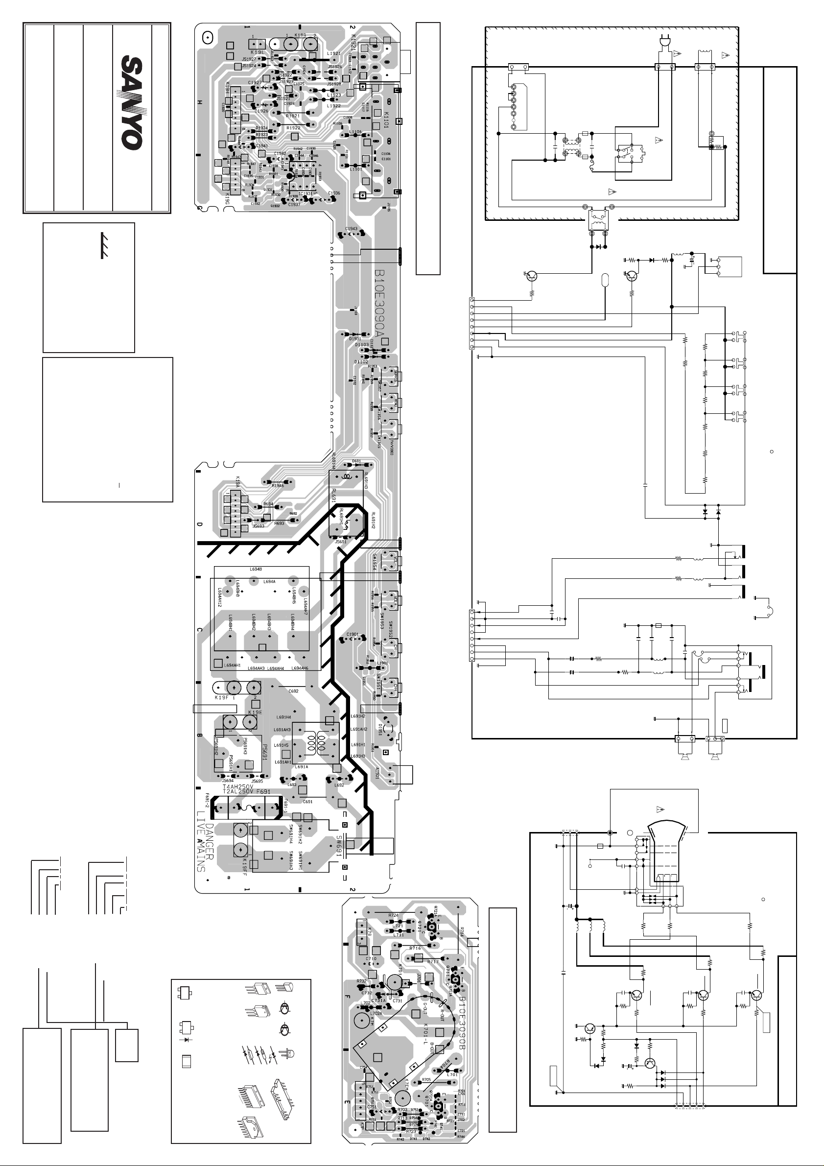
ASSY,PWB,FRONT C3YFV (1AA0B10E661BA)
PWB,FRONT C3AC (1AA4B10E3090A)
AT3AT3AT3AT3
AT3
AT3
AT3
TO_MAIN
KA
J11EH080N
K19A
1
8
POWER&
RL
KEY
RC
9V
LED 1
RC5V
GND
Q692
8.2K
R694
D1951
DLXRB0001653C
9V
Q1951
R1952
1/16GJ
47KC
1/16GJ
1.5KC
R1953
C1102
KK1000GQ
R1101
1/16GJ
2.2KC
330C
1/16GJ
R1960
1/16GJ
15KC
1/16GJ
8.2KC
1/16GJ
4.7KC
1/16GJ
2.7KC
1/16GJ
2.2KC
1/16GZ
0C
R1954
R1955
R1956
R1957
R1958
R1959
1SS133
D1103
AMP
RC
D1102
1SS133
A1901
U20B20900
SW1951
1170N
S10B
SW1952
1170N
S10B
- ++-
SW1953
1170N
S10B
VOLCH
SW1954
1170N
S10B
A4B10E30900
:A4B10E3090A
PB1901
TO_MAIN
KH
KK1000
GQ
C1929
GND
8
AV3-R
GND
AV3-L
GND
AV3-V
GND
L-IN
1
R-IN
J11EH080N
K19H
J10EA030N
K7Q
250EM22
CY
3
C710
KK1000
GQ
16PM
10P
16PM
10P
TO_MAIN
KQ
C1928
C1926
C1927
1
0250N
L721
J
J30B
K7D1
KK0.01
GQ
1/2
DJ150
R1922
1/2DJ150
1AA0W31B07300
W902
L702A
Z20103---
K7M
J30B0250N
C731
2000KZ
1000HE
L701
L711
J
J
C1925
R1921
GQ
275
-41
9
10
KK0.01
2.7K
2.2KC
L1921
Z21B0040N:
Z21B0710B
KK0.01GQC1923
C1924
L1922
L2C1120JN
L1923
L2C1120JN
:A10B15000
AT1
R717
1/2DJ
1/2DJ
2.7K
R716
1/16GJ
R1106
KK0.01GQC1922
J30B0250N
1
SP902
A10B22200
11
8
6
9100
L1101
L2B
KN
9100
L1106
L2B
KN
JS1928
J
K19R-2
J30B0250N
K19R-1
L-OUT
R-OUT
(W76EGV023X115)
BXXAVB114VIU
Q901
J11B3090N
K701-L
J31B01000
K1101
LRV
JS1929
J
J10EA020N
K19L
1
:A10B15000
A10B22200
SP901
A4B10E30900:
A4B10E3090B
1/2DJ
2.7K
R705
PB701
2SJ
12K
R704
1/16GZ0C
JS1923
J12B05400:
J12B04901
K1921
Q701/Q711/Q721
QT0392
QT0392
QT0392
R714
2SJ
220C
D752
1/16GJ
D753
KP
Q711
R711
D754
TO_MAIN
R-OUT
470
1
12K
R713
050N
K7P
J10EA
GQ
220C
KK560
1/16GJ
R701C701
470
R703
C732
KK1200
Transistor
B
C
E
Diode
A
123
12 x 10
3
= 12k
K
Resistor
B
C
E
B
C
E
K
1
2
3
9
10
1
2
3
4
5
6
7
K
A
A
N
E
C
B
B
C
B
E
A
K
1
E
C
N/2
N/2 + 1
Q741/Q751
2SA1037AKR:
2SA1179NM6P:
TXXKBB001P:
TXXKBB002P:
TXXKBB003P
TP-7E
680C
1/16GJ
R744
0C
0C
1/16GJ
1.2KC
Q741
1/16GZ
D741
D742
1/16GZ
GQ
R741
C721
KK560
1/16GJ
5.6KC
330CD
1/16GJ
10KC
R742
16EM
R753
220C
C751
1/16GJ
0C
R721
1/16GZ
R751
12K
Q721
470
R723
1SS355
D751
Q751
R724
2SJ
G-OUT
1/16GJ
10KC
R752
KK560GQC711
5
1SS3551SS355
1SS355
1AA4B10E3090B PWB,SOCKET,C3AC
1AA0B10E661BB ASSY,PWB,SOCKET,C3YFV
B-OUT
Q701
TP-7B
Page 2
MAIN BOARD
JW11
JW12
JW13
C3132
10
R625
R627
C3122
12
11
R3129
R3128
J603
C614
R024
J609
C639
C3123
J544
J607
D633
R3417
J546
C3133
L3469
J538
J653
J655
J654
J656
J657
R874
R875
J620
D615
C635
J536
J537
Q611
J517
R646
L641
R645
C823
J434
R642
J407
1
J406
Z13
D616
R611
L861
R647
J601
JW18
R644
4
R624
R628
R864
R626
Z31
R002
R001
C015
R021
2
IC001
10
C009
C013
C007
Q001
R013
R023
J554
Q044
J542
J541
R821
R822
R830
R829
C834
J533
X801
C833
R832
R831
R840
R852
R853
R860
C811
J630
C810
C861
C826
C824
29
J633
R885
J616
Q808
D646
IC641
C637
R641
VR641
Q641
R689
2
Q686
R688
3
R622
D614
R619
D617
JS611
L611
R014
R016
J651
C002
C001
1
C005
11
C011
J649
R003
C003
R004
C004
R008
C006
R007
F001
R005
R006
C008
C021A
R010
C021
R009
C012
R022
J652
J644
PB1
1
KH
J648
J647
1
KG
J623
Z32
R018
J646
R827
R826
J641
56
49
Q879
10
R879
IC801
40
C819C818 R839
C803
C822 R842
C807
C817
R838
C816
J635
C802
8
5
R872
C801
IC803
R871
JS617
1
4
J617
D641
R884
J618
IC643
C648
C649
IC642
R643
E
Q661
R661
D645
D685
C685
Q685
R637-1
R687
KF
R602-2
C604
C606
J622
J621
R824
R823
R817
J643
J637
R815
1
C827
J642
R863
Q807
J639
R862
R861
R819
D826
R818
R808
J636
R881
R653
R654
R880
20
C835
D637
D638
J634
R809
28
L803
L802
J632
R870
L801
R873
J615
J631
D647
J619
1
C650
KA
R681
R648
R659
C682
Q645
R660
Q682
C666
R667
J610
R686
R637
Q666
R666
D666
E
R637-2
Q666A
C636
X
D683
R663
JS637
12
KF-2
KF-1
XX
XX
KGG-2KGG-1
C603
R602-1
R602
D603
D604
D605
C605
C607
R620
R621
1
D606
HT
HT
C612
C613
C607-2C607-1
D1002
R1201
C305
Q1043
E
L432
D439
T451
L102
J236
J233
J237
L1204
J224
J223
C1043
R440
T451-6
30V
JS105
Q1205
C1042
R1219
R1220
Q431
J201
5
R138
L1202
JS301
J312
R1224
R153
C1214
C306
J205
J311
D438
C421
NC
J242
J241
J246
C432
J202
T451-5
J244
8
J217
J240
1
Q1203
T431
JS107
D101
Q153
IF
R137
C1202
T451-4
R308
R307
Q1206
C433
R152
R214
R215
R1215
D1041
D1042
R434
R432
C431
X
KDY-1
T451-3
Q1202
R1218
R1216
R1225
C1201
J218
T451-1
R146
D132
R147
R145
C138
R144
R157
Z04
C421-2
R443
1
2
JS132
1
C136
R139
R149
Z03
R143
IC301
C1217
R859
C815
C423-2
R466
R148
J340
JS202
10
9
JS806
R1034
R858
C434
Q432-C
J336
16
Q432-E
KDY
R150
C145
J323
Q141
JS131
C123
L201
R855
Q432
C446A
T451-2
J245
J243
D131
J355
R1217
J308
R302
Q806
Q805
R510
C137
J322
JS111
C124
L431
C446
C131
C208
J328
R301
KDY-3
X
JS108
C140
C1207
X
R158
L243
J203
R140
C132
C133
R141
C238
C232
C215
J326
Q301
C814
C423
3
C446-1
C446-2
C446A-2
C106
Q133
R142
C127
L103
Q152
C144
C239
C230
R256
R257
L242
R854
C501
IC501H3
X131A
Q151
X132
C207
R303
J307
Q432-B
Q132
C134
JS104
C128
R135
T131
J335
R136
C120
C135
C146
C203
R201
C209
C201
C202
65
C125
X131
C121
70
80
110 2024
X231
C231
C126
R233
R238
R230
C235
R234
C233
C236
J327
R240
R239
Q242
C237
R242
J325
R243
R241
J324
Q243
Q244
R848
J344
J343
R258
J247
L244
KP
J248
1
J314
R849
R304
R309
J351
J313
J310
J309
J305
J304
J303
R857
R856
J423
J424
R217
J425
Q804
J301
R437
C527
R514
D501
R537
10
C503
R534
R512
R503
L501
C529
D449
R449
R459
R467
R476
R475
C511
C423-1
KDY-5
KDY-6
X
X
6
5
Q425
R461
R442
L443A
C443-1
C441-1
C443-2
C441
X
C441-2
L443
C443
X
X
C442
C442A
X
C451
J334
J333
64
IC201
C234
R462
R464
C528
R511
L441
R134
C130
R161
L124
Q424
D464
R487
D465
C161
R209
C210
R251
D463
R847
D503
D422
R460
D423
C443A
C443A-1
C437A
C437
R132
R264
C223
25
R247
R246
C242
L231
R843
R844
R845
R851
C502
R518
R513
C504
R516
D502
C441A
C441A-1
L461
J302
R133
C206
5060
30
C214
Z10
C428
L461A
Q131
C301
R542
C261
C243
IC501
C505
D504
L122
C222
R248
C429
R477
L442-1
C139
X121
JW19
C3402
R3411
J524
R523
C217
C212
J522
R3486
R3476
Q3453
R3474
C3441
R3441
C3442
R3442
R491
R657
C427-1
J504
C483
Z21Z22
R632
R473
Q3455
C3443
C3444
Q491
R469
C3417
Q3452
C463
C3419
R3488
L643
D3418
C3416
C3413
JS3503
R3413
L3457
C3484
L3456
D461
C462
C3418
C3421
C3485
Q3454
R3473
C686
J527
R3412
R3414
R3475
D648
C486
C3408
C3490
C3488
R3487
R3485
D3441
R3443
R3444
R103
Z01
R656
R650
R655
Z02
TP-B
C642A-1
Q461A
D460
13 20
24
C3481
C3480
C3477
D3442
T611-8
E
C113
C3401
C3129
J516
X
T611-11
Q462
C3403
IC3401
C3415
R3133
64
60
R3471
40
33
R492
C642
Q461
R471
D466
C468
R468
50
L632
C3414
C3126
D3121
Q642
C642A
T611-12
C3406
C3409
C3404
R3127
C3405
12
C3407
10
J553
C3411
C3412
R3134
1
R3403
C3128
C3420
C3127
R3132
L3121
J548
C3456
J549
C3452
R3453
C3453
C3454
J547
C3462
C3489
C3493
C3492
C3494
C3495
C3483
C3482
IC3451
D041
C3476
C3431
C3432
D3443
C3433
R3415
C3436
D3444
C3434
R3416
J515
R658
R652
R651
R636
Q643
C633
E
R649
J306
C642A-2
D630
C646
L642
T611-13
T611-5
LIVE MAINS
Q613-B
C631
R631
R048
C010
Q043
J521
C3131
C3121
C3124
J552
L3122
J551
30
33
34
22
23
20
PB
PB
40
IC3121
1
44
R3131
R3121
JS3452
1
JS3451
J543
C3458
R3452
C3461
10
20
C3435
32
C3459
C3467
C3446
C3447
L3459
J608
J606
X3451
L3452
R3451
C3460
R3126
R3123
R3122
C651
J605
Q651
E
C640
D643
D635
D642
D644
C641
L635
T611-17
T611
C647
T611-2
T611-3
DANGER
C615
D618
D619
R623
Q612
R615
R617
L612
Q613
Q613-C
Q613-E
C617
X
C616B
C616A
C616
R3124
Z16
R130
C129
R129
R128
R123
JS109
Q121
L121
R124
R127
Q162
R163
C263
C262
R165
C216
R213
C221
C241
C219
41
R263
J341
C213
40
R231
J339
Q122
R131
R126
R164
J338
R162
Q161
C224
R216
C218
JS3504
J342
R219
C220
J332
R212
J331
Q211
R232
Q231
R218
R254
R202
R255
C251
J329
J416
J414
R253
J330
R250
J418
J421
J422
J512
J431
J510
J435
R546
J316
R515
R483
R547
Q532
J436
J432
1
R502
C506
C506A
C687
R517
JS501
J433
D431
C426
R436
IC501H2
J200
C436
C427
X
L442-2
JS114
R455
R441
R454
R435-1
L442
J506
J503
R435
J502
R486
R435-2
R472
R470
R474
R463
D469
R465
R488
C450
C470
R450
J114
C112
C1031
C108
TU
AGC
ADR
R101
C057
C056
J113
D1051
1
KCPA
C101
X
KEM2
C102
K1003
R1015
C1038
5
R1014
R1049
L1012
C1017
5
R1031
R1032
L1003
K1001
D1019
20
C1016
J104
J102
L1019
L1018
R1207
C1200
J105
L1205
C1044
20
R1002
D1003
R1005
R1007
R1009
10
R1011
R1012
C1034
C1013
C1014
D1018
R1018
D1021
L1017
R1017
R1048
R1019
D1044
D1047
D1046
R1050
10
R1020
R1021
J110
J111
C1046
C1047
15
C1033
K1002
15
C1037
L1022
C1036
1
C1035
R1022
R1023
J109
C053
C435
C466
R1206
J230
C1213
C1011
R1013
C1111
D1043
C1045
D1007
D1008
L1010
C1010
C1012
C1015
JW16
R102
SCL
C104
X
J106
J103
R1042
D1010
R1016
J221
R1047
L1020
L1023
C1212
J232
C1204
R1043
L1013
J211
C1029
C1027
R1001
SDA
J108
TP-A
C1218
D1203
L1201
Q1041
1
L1011
IC1401
8
R1226
D1026
D1025
X
C424A
J107
R1203
C052
C1215
J214
J213
J212
J215
J216
C1021
J225
C1024
C1028
C109
L101
J337
R835
R834
C1205
L1206
R1230
Q1042
J226
J222
C424
C107
MB
C103
R1003
J220
C1026
Q802
C149
Q1044
L1021
J219
A101
R154
R1041
J229
J227
X
BP
NC
C110
J239
IC1201
9
C1203
C1211
J231
1
Z33
R1227
L301
D1202
C303
J228
16
D1022
C1020
10
9
R1046
R1044
R433
D1052
J206
C438
R445
C422A
C422
JW17
C465
L462-1
L462
L462A
L462-2
KQ
3
C482
R482
2
1
1
R452
R448
D442
R451
T451-11A
R456
C447
Q447
D441
R481
C445
KSC
X
T451A-11
T451-11
D446
D445
R447
R458
R457
D448
R453
PB
T451-11B
C421-1
Z09
Q451
3
4
R444
D481
D482
R480
T451-10
T451A
T451-7
7
T451A11A
Page 3

TO
Part No. SKP20370 C3YFV (SHEET 2-3)
FRONT
K19H
KH
J10EF080N
1
2
3
4
5
6
7
8
R SP
L SP
27V
C021A
35EM
1000CD
R014
DJ680
AV3-V
AV3-L
AV3-R
R016
DJ680
C012
25EM
2200CD
C011
25EM
2200CD
PB101
A4B10E30800
-
P_
+
R SP AMP
+
R_
L SP AMP
VCC
1110987654321
F001
J
C009
25KZ
0.1GQF
C013
Z31
25KZ
2400010
0.1GQF
Z32
R010
2400010
4.7
C008
25KZ
0.1GQF
C007
25KZ
0.1GQF
R009
4.7
PW
GND
R006
1.5K
R008
1.5K
C003
16KK0.47
(BA:GMB)
-
R004
1/16GJ
1KC
R003
1/16GJ
3.3KC
C006
25EM
33CD
KK0.012
Q043
R007
47
C004
GQ
25EM47CD
C010
16EM
100CD
1/16GJ
560C
C015
D041
1SS133
R023
1AA0HEA0100--
pre
GND
C005
25EM
33CD
R005
47
R001
1/16GJ
3.3KC
R013
1/16GJ
2.7KC
+9V
IC001-1
R048
1/16GJ
10KC
Q044
TDA7263M
C002
C001
16KK0.47
(BA:GMB)
Q001
R024
2.2K
IC001
KK0.012
GQ
R002
1/16GJ
1KC
R018
1/16GJ
10KC
R022
1Q001/Q044
2SC2412KR:
2SC2412KR:
2SC2812NL6P:
2SC2812NL6P:
TXXKBB004P:
TXXKBB004P:
TXXKBB005P:
TXXKBB005P:
TXXKBB006P
TXXKBB006P
1/16GJ
47KC
C3401
25EM4.7CD
Q043
2SA1037AKR:
2SA1179NM6P:
TXXKBB001P:
TXXKBB002P:
TXXKBB003P
C3409
25EM4.7CD
JS3503
J
JS3504
L3456L3457
MOL
SCL
C3485
KK0.01
GQ
C3484
6.3EM
47CD
C3493
KK0.01
GQ
MOR
SDA
R3452
100
L2B9
2R2KN
C3494
25KZ
0.1GQF
DDA3SSA1
V
V
C3452
16KK
0.47BA:
16KK
0.47GMB
AUXOL
DDA1
V
1/16
GJ10KC
C3495
25KZ
0.1GQF
R3453
AUXOR
Iref
C3483
KK0.01
GQ
DDA3
V
P1
C3453
CJ
47
CGQ
Q3454/Q3455
2SC2412KR:
2SC2812NL6P:
TXXKBB004P:
TXXKBB005P:
TXXKBB006P
C3482
KK0.01
GQ
PCAPL
PCAPR
SIF2
Vref1
C3454
25KZ
0.1GQF
R3487
1/16GJ
470C
C3481
6.3EM
47CD
Vref3
SIF1
C3458
CJ
47
CGQ
Q3455
R3488
1/16GJ
2.2KC
R3485
1/16GJ
470C
SCOL2
SCOR2
SSD1
ADDR2
V
L3459
1/16GZ
0C
C3459
6.3EM47CD
R3486
1/16GJ
2.2KC
SSA4
V
DDD1
V
L3452
L2B9
2R2KN
SSD2
V
CRESET
C3461
16KZ1FA
Q3454
6.3EM
47CD
SCOL1
SCOR1
XTALO
XTALI
X3451
V10B
2830N
24.576MHz
C3480
5V-1
R3475
1/16
GJ470C
Vref2
Vtune
Q3453
CAPR1
P2
R3476
1/16
GJ2.2KC
CAPR2
SYSCLK
43444546474849505152535455565758596061626364
SSA2
V
SCK
L2B9
2R2KN
C3489
KK0.01GQ
R3411
1/16GZ
0C
R3413
1/16GZ
0C
C3492
KK0.01
GQ
LOL
DDD2
LOR
V
IC3451
TDA9875A/V2
PCLK
NICAM
ADDR1
12345678910111213141516171819202122
R3451
100
J
TO
FRONT
K19A
KA
J10EF080N
RELAY
1
2
3
+9V
4
5
SPARK
6
7
8
IC803
CAT24WC08P:
M24C08-BN6:
24LC08B/P
1
2
3
45
R861
1/16GJ
680C
D826
MTZJ4.3B
8
7
6
Q807
R862
1/16GJ
8.2KC
R863
1/16GJ
15KC
L801
L2B95R6KN
16KZ2.2FA:
16KZ2.2GWF
R809
1/16GJ
10KC
C801
KK0.01
GQ
Q807
2SA1037AKR:
2SA1179NM6P:
TXXKBB001P:
TXXKBB002P:
TXXKBB003P
C827
R873
1/16GJ
3.9KC
R847
1/16GJ
4.7KC
R848
1/16GJ
4.7KC
R849
1/16GJ
4.7KC
R872
1/16GJ
3.9KC
5R6KN
L802
L2B9
R871
1/16GJ10KC
C802
10EM47CD
L803
L2B95
R6KN
R843
2.7K
R844
2.7K
R845
2.7K
R875
R870
1/16GJ
100C
470
R874
C803
25KZ0.1
GQF
C807
C816
KK4700
GQ
R880
470
1/16G
J39KC
R881
1K
R851
J
25KZ
0.1GQF
C817
CJ22
CGQ
KK1000
R808
100
C821
R815
100
R824
100
R823
100
C835
KK4700
GQ
R838
1/16GJ
5.6KC
IC801
QXXAVC007---N
1
RC IN
RESET
2
OUT
3
50/60
4
H-BLK
5
V-BLK
6
AV SW2
7
AV SW1
8
KEY IN
9
H-P
RELAY
10
11
Protect
12
HP-MUTE
13
BBE
14
15
B-OUT
16
G-OUT
17
R-OUT
18
FB-OUT
19
SDA
20
SCL
21
VDD
22
23
24
25
AVDD3
26
TEST0
27
MCFM
28 29
8Pin
(SC1)
8Pin
(SC2)
POWER&RL
P-TTARI
AGC
H-PHASE
S-VHS SW
LED
Mute
IGNOR
STATUS
ACK
V-SYNC
H-SYNC
VDDA
PXFM
AVDD2
TXCF
L/L'
56
55
54
53
52
51
50
X801
EX0046XC:
EX0046SC
49
48
47
46
45
44
43
42
41
40
39
38
37
36
35
34
33
32
31
30
1/16GJ
33KC
R884
47K
R842
1/16GJ
15KC
R829
Q808
C834
CJ27
CGQ
R817
100
1/16GJ
33KC
C824
R830
CJ82
CGQ
D1051
UDZS10BG
R826
220
C833
CJ27
CGQ
Q808
2SC2412KR:
2SC2812NL6P:
TXXKBB004P:
TXXKBB005P:
TXXKBB006P
C819
CJ22
CGQ
C826
PM
0.47P
C861
CJ150
CGQ
C822
KK2200
GQ
R831
1/16GJ
10KC
R839
1/16GJ
5.6KC
C818
KK4700
GQ
R860
1/16GJ
270C
R852
1/16GJ
27KC
R832
1/16GJ
10KC
1/16GJ
1KC
R853
1/16GJ
22KC
R840
R885
1K
KCPA
J10AN050N
1
R821
J
R822
J
R834
47K
2SC2412KR:
2SC2812NL6P:
TXXKBB004P:
TXXKBB005P:
TXXKBB006P
L861
L2B95R6KN
Q802
+5V
JS806
1/16GZ
R835
3.9K
0C
R859
1/16GZ
0C
R143
1/16GZ
0C
R144
1/16GJ
220C
C138
KK0.01
GQ
R145
1/16GJ
68KC
C131
KK0.01
GQ
1SS356
R147
1/16GJ
10KC
R148
1/16GJ
10KC
R149
56
Q152
2SC2412KR:
2SC2812NL6P:
TXXKBB004P:
TXXKBB005P:
TXXKBB006P
Q121/Q162
2SC2412KR:
2SC2412KR:
2SC2812NL6P:
2SC2812NL6P:
TXXKBB004P:
TXXKBB004P:
TXXKBB005P:
TXXKBB005P:
TXXKBB006P
TXXKBB006P
1/16GZ0C
R146
1/16GJ
22KC
D132
JS109
Q141
2SC
2814F4P:
2SC
2814-F5
R139
1/16GJ
27C
D131
1SS356
R150
1/16GJ
33KC
+5V
DJ27B
1/16GJ
47C
1/16GJ
5.6KC
R142
1/16GJ
1KC
Q151
2SC2412KR:
2SC2812NL6P:
TXXKBB004P:
TXXKBB005P:
TXXKBB006P
Q152
16EM47CD
R164
1/16GJ
1KC
Q121
R127
1/16GJ
560C
R123
C106
KK0.01
GQ
R140
R141
C136
KK0.01
GQ
L103
C120
J
Q162
R163
1/16GJ
2.7KC
R124
1/16GJ
2.7KC
+9V
C132
CC5CGQ
C133
CC5CGQ
C143
1/16GZ
0C
R152
27K
T131
SL0004XV
X131
SB6315T
C127
KK0.01
GQ
L124
J
C146
16EM47CD
1/16GZ0C
C134
CJ82
CGQ
X132
SF5315
:SF5315U
C121
KK0.01
GQ
C125
16EM10CD
C203
16KK0.47BA:
16KK0.47GMB
R201
1/16GJ
C202
470C
KK22
00GQ
KK0.01
GQ
C130
JS104
1/16GZ0C
Q133
2SC2412KR:
2SC2812NL6P:
TXXKBB004P:
TXXKBB005P:
TXXKBB006P
C135
R154
1/16GJ
10KC
R158
1/16GJ
39KC
1/16GJ
100C
80
79
78
77
76
75
74
73
72
71
70
69
68
67
66
65
R136
+5V
R157
1/16GJ
10KC
C123
KK
0.01GQ
C144
16KZ1
FA
C140
C124
FK0.01BE
16EM10CD
12345678910
IF-AGC
PIFVCO
FIL
C232
CC10
CGQ
RIPPLE
C238
CC1
CGQ
1/16GJ
33KC
PIF-IN
PIF-IN
RF-AGC
NC
SIF-IN
SIF-IN
IF-VCC-5V
SIF-IN
IF-GND
SIF-OUT
DC-NF
LOOP-FILTER
IF-DET-OUT
IF-VCC-9V
DAC3
C128
10EM
220CD
R137
1/16GJ
470C
R138
1/16GJ
470C
AU-TV-OUT
DE-EMP
R153
1/16GJ
470C
Q133
R209
1/16GZ0C
C209
16KZ
1FA
Q153
2SA1037AKR:
2SA1179NM6P:
TXXKBB001P:
TXXKBB002P:
TXXKBB003P
DC-RESTOR
Y/CVBS1-IN
C210
16KZ1FA
R264
1/16GJ
100C
R230
X231
V10B
2961N
X-TAL
YS
KK22
00GQ
C231
C230
16KK0.22BA
APC
FILTER
C-IN
KK0.01
GQ
C206
C126
16KK0.47
(BA:GMB)
R-IN
25KZ0
S-FILTER
B-IN
.1GQF
C261
25KZ0
.1GQF
C262
G-IN
55565758596061626364
1FA
16KZ
C263
2
C614
HJ0.1G
R619
1/2DJ
47
D617
ES1(:Z)
1/16GJ
22KC
34
R626
DG
2.2K
R615
1
R622
DJ
15K
L611
L2E9220KN:
L2E7220KN:
L2J4220KN
TO
FRONT
K19F
KF-1
J30B
0250N
KF-2
J30B
0250N
Q611
R602
5WK1.8V:
5WK1800K
R602-1
2400010
1000KK
1000
(CBB:HB)
1000KK
1000
(CBB:HB)
2SA1037AKR:
2SA1179NM6P:
TXXKBB001P:
TXXKBB002P:
TXXKBB003P
D603/.../D606
R602-2
2400010
C603
C604
D616/D618
1SS133
1SS133
ERC05-10B
:RM11C
D605
D603
D604
R611
1/16GJ
5.6KC
Q611
D619
MTZJ
11B
R623
1/16GJ
1.5KC
D606
D618
D616
1/16GJ
1.2KC
D615
PC123F2
C607
400EM220
R617
(XD:XN)
C607-2
2400010
C607-1
2400010
:ERA18-04
R628
2SJ56
Q612
2SC3807
RYA
C615
FJ0.015
(BE:D)
R620
1/2DJ
120K
R621
1/2DJ
120K
D614
1SS133
R624
2SJ47
L612
L3004
R625
2SJ22
C616
2000KK
2200
(CTB:NH)
Q613
2SC4429LYB
:2SC4429MYB
2400010
Q613-B
C617
FK0.033
(BE:D)
R627
2SJ22
Q613-1
0HEA0099--
Q613-C
2400010
2400010
Z13
2400010
Q613-E
Z16
2400010
R631
1/2CK
5.6MXG
:1/2XJ
5.6MVA
T611-3
2400030
T611
L51B4850N
T611-2
2
17
2400030
3
16
15
T611-5
5
2400030
18
6
14
7
13
12
11
T611-8
2400030
810
R632
1/2CK
5.6MXG
:1/2XJ
5.6MVA
C631
400KM2200XS
:400KK2200XP
:250KK2200XH
C682
R681
R660
10K
1/16GJ10KC
R651
DJ10K
145V
R689
1/16GJ22KC
R688
1/16GJ
10KCQ686
D685
MTZJ6.2B
R658
10K
16EM
33CD
Q645
2SC2412KR:
2SC2812NL6P:
TXXKBB004P:
TXXKBB005P:
TXXKBB006P
Q661
2SB764E:
2SA1020Y
R661
R637
5WK2.2V
R637-1
2400010
Q651
2SB985(S:T):
2SA1707(S:T)
Q685
C685
EM1CD
Q682
2SC2412KR:
2SC2812NL6P:
TXXKBB004P:
TXXKBB005P:
TXXKBB006P
R663
1/2DJ
390
R637-2
2400010
R652
DJ3.9K
D683
1SS355
R686
1/16GJ
220KC
R687
1/16GJ
560KC
Q685
2SC2412KR:
2SC2812NL6P:
TXXKBB004P:
TXXKBB005P:
TXXKBB006P
R653
1/16GJ
22KC
R654
1/16GJ
6.8KC
27V
D637
1SS133
R644
2SJ18
R648
2SJ22
R643
J
IC642
BA178M09T
:MC78M09CT
:UPC78M09AHF
123
C649
16EM
100CD
IC641
BA178M05T
:MC78M05CT
:UPC78M05AHF
:L78M05CV
321
C648
6.3EM
100CD
IC643
BA178M05T
:MC78M05CT
:UPC78M05AHF
:L78M05CV
123
C651
6.3EM
1000CD
C650
6.3EM100CD
1SS355
D646
1SS355
C139
6.3EM47CD
D647
1SS355
L3469
J
D641
+9V
+5V
C137
KK
0.01GQ
5V-1
TECT
PRO
R646
DJ
150K
R659
1/2DJ
68K
R645
DJ22K
C687
25EM
1000T
1/16GJ
10KC
R647
1/16GJ10KC
Q666
R666
2SC3807RYA
1/2DJ18
R667
D635
RU4YXLF-L1
D630
EU2(:Z):
D642
ERB44-02
RU4AMLF-L1
C642A-2
2400010
C642A-1
2400010
C642
200EM220XD
D648
RU3YX
R649
10K
2SA1037AKR:
2SA1179NM6P:
TXXKBB001P:
TXXKBB002P:
TXXKBB003P
560
C666
16EM47CD
D633
ERC91-02L
C637
35EM
2200CD
R642
NF150K
R641
1/16GJ
6.2KC
C686
25EM
470CD
R650
100K
MTZJ5.6B
C640
25EM
2200CD
R636
10K
C633
25EM
470CD
2SC2412KR:
2SC2812NL6P:
TXXKBB004P:
TXXKBB005P:
TXXKBB006P
VR641
R3L1202NJ
:R3D7222NJ
R656
100K
D666
1SS355
Q643
D644
1SS355
D643
Q641
D645
MTZJ6.2B
Q642
2SC4487(S:T):
2SD1347(S:T)
R655
DJ2.2K
R657
1SJ3.3
C647
KK680GQ
T611-17
2400030
L635
ZZ0122
L641
J
L632
J
L642
J
T611-13
2400030
T611-12
C641
2400030
1000KK1500
(NH:CTB)
T611-11
2400030
L643
J
Q643/Q686
Page 4

Q3452/Q3453
2SC2412KR:
2SC2812NL6P:
TXXKBB004P:
TXXKBB005P:
Q3452
D3441
UDZS10BG
DDA2
V
SCIL2
SDI1
TEST1
+9V
R165
1/16GJ
1KC
R162
1/16GJ
2.2KC
R257
1/16GJ
1KC
Q243
TXXKBB006P
C3431
CJ100
CGQ
D3442
UDZS
10BG
SCIR2
MONO_IN
R3415
1/16GJ
15KC
C3467
16KZ1FA
AM
C3447
16KK
0.33BA:
16KK
0.33GMB
R258
1/16GJ
1KC
Q242/Q243/Q244
2SA1037AKR:
2SA1179NM6P:
TXXKBB001P:
TXXKBB002P:
TXXKBB003P
Q244
YC-GND
1/16GJ15KC
C3432
UDZS
10BG
SSG
V
TEST2
C3435
CJ100
CGQ
1/16GJ
10KC
VM-OUT
R3441
D3443
1/16GJ
100C
R233
SCIL1
EXTIR
DAC1
CJ100CGQ
C3433
CJ100CGQ
33343536373839404142
SCIR1
EXTIL
R234
YSM
D3444
UDZS10BG
R3416
1/16GJ
15KC
C3436
CJ100
CGQ
C3446
16KK
0.33BA:
16KK
0.33GMB
R3442
1/16GJ15KC
C3434
CJ100
CGQ
25KZ0.1
C235
R-IN-CPU
C3441/3442/
C3443/3444
16KK0.33BA:
16KK0.33GMB
R3443
1/16GJ15KC
R3444
1/16GJ15KC
GQF
25KZ0.1
GQF
C236
G-IN-CPU
B-IN-CPU
C3129
KK
0.01GQ
R3473
1/16
GJ470C
R3474
1/16
GJ2.2KC
C3476
16KK0.47BA:
16KK0.47GMB
R3471
C3477
1/16
6.3
GJ
EM47
270C
CD
Vref(n)
CAPL1
SDO2
R240
1/16GJ
2.2KC
R242
1/16GJ
2.2KC
R-OUT
1/16GJ
1KC
R239
1/16GJ
100C
Vref(p)
SDO1
SDI2
Q161
2SC2412KR:
2SC2812NL6P:
TXXKBB004P:
TXXKBB005P:
TXXKBB006P
R161
100
C161
KK
0.01GQ
R256
Q242
R241
1/16GJ
100C
R243
1/16GJ
100C
G-OUT
B-OUT
CAPL2
WS
23 24 25 26 27 28 29 30 31 32
R238
1/16GJ
2.2KC
L201
J
C207
KK0.01
GQ
C208
16EM
47CD
11 12 13 14 15 16 17 18 19 20 21 22 23 24
YC-VCC-5V
IC201
TB1262FM
Y/MON-OUT
BLACK-DET
R213
1/16GJ
100KC
2SA1037AKR:2SA1179NM6P:
TXXKBB001P:TXXKBB002P:
1/16GJ
1KC
C216
16EM10CD
Q211
TXXKBB003P
IC501
LA7846N
VCC
OUT
GND
IC501H3
2400010
IC501H2
2400010
0HEA0072--
CB-OUT
R218
IN
IC501-1
CR-OUT
Q211
C501
10
9
8
7
6
5
4
3
2
1
DIG-GND
C223
KK0.01
GQ
JS107
1/16GZ
0C
25EM
1000T
L26B0800N:
L26B4410N:
L2G33R3KN:
L2PC3R3KN
C511
100FK
0.033AD:
100FK
0.033BE
CR3-IN
R515
1FJ3.3
C502
35EM220CD
D501
EM01Z:
ERA15-02
C505
L501
CB3-IN
C222
+5V
500CD
8GAA
R512
1SJ470
KDY-6
J30B
0250N
KK0.01
GQ
JS501
R513
1/16
GZ0C
V-OUT
J
R542
1/16GJ
10KC
KDY-5
J30B
0250N
R503
1/16GJ
56KC
V-RAMP
C241
HJ0.47
R514
1/16GJ
6.8KC
J30B
0250N
R502
1/2FJ1.5
C506
HJ0.47
KDY-3
H-VCC
C221
KK0.01
GQ
R492
1/16GJ
10KC
R518
1/16GJ
47KC
16KK
0.33
(BA:GMB)
R510
1SJ
0.68
KDY-1
J30B
0250N
Y3/CVBS3-IN
C219
KK5600
GQ
Q491
R534
1/6NF
5.6K
C504
C528
25KZ
0.1GQF
H-AFC
R491
1/16GJ
2.7KC
R516
6.8K
SYNC^OUT
C220
EM1CD
VD
1/16GJ
10KC
D502
1SS355
C237
25KZ0.1
RGB-VCC-9V
HD-SCP
4142434445464748495051525354
R216
1/16GJ
4.7KC
R523
J
R537
D503
MTZJ
6.8B
GQF
C3441
C3443
SCL
SDA
EHT-IN
ABCL-IN
BED-PIN
EW-OUT
CW-OUT
DIG-VCC
DAC2
FBP-IN
H-OUT
R263
1/16GJ
10KC
1/16GJ
4.7KC
Q804
C503
KK0.01
GQ
R517
1/16GJ
27KC
C3442
C3444
L231
25
26
27
28
29
30
31
32
33
34
35
36
37
38
39
VD
40
C212
KK1000
GQ
P-TTARI
Q491/Q804/Q805
2SC2412KR:
2SC2812NL6P:
TXXKBB004P:
TXXKBB005P:
TXXKBB006P
R856
1/16GJ
4.7KC
R855
1/16GJ
10KC
C814
KK3300GQ
D504
1SS355
C529
16EM10CD
J
C242
16KZ
1FA
R212
270
C224
KK1000
GQ
R854
C233
16EM47CD
R215
R214
C251
16KZ
1FA
R247
1/16GZ0C
R248
1/16GJ
82KC
C218
KK0.01
GQ
CJ330CGQ
+9V
Q805
D449
EM01Z:
ERA15-02
100
100
1/16GJ
120KC
R202
1/16
GJ
27KC
C243
16KK
0.47
(BA:GMB)
C213
16EM47CD
C141
PRO
TECT
C234
25KZ
0.1GQF
R251
R253
100K
R246
1/16GJ
39KC
R254
100K
R857
1/16GJ
33KC
D463
1SS133
C438
KK1000GQ
R255
1/16GJ
56KC
R250
4.7K
ABCL IN
R464
J
J10EA050N
KP
1/16GJ
5.6KC
R486
1/2DJ47K
C486
160EM
0.47CY
TO_SOCKET_K7P
+9V
FBP
H OUT
R437
330
R434
R217
10K
R432
1/16
GJ1KC
C431
16KK
0.47
(BA:GMB)
12345
L244
L2B92R2KN
D431
MTZJ9.1B
1/2DJ
1K
Q431
2SC
3332
(R:S)
C467
16KZ
1FA
L243
L2B92R2KN
L242
L2B92R2KN
A101
F1BEB0250
TUNER(WITH PLL & BAND SW)
13 14
GND
12
IF1
BT
N.C
BP
MB
DATA
CLOCK
C102
6.3EM
470CD
R445
100
R436
DJ10K
R433
C433
500KK
3900A
145V
Y IN
1
2 3
R462
J
R488
1/16GJ
470KC
R103
1SJ33K
JS202
1/16GZ0C
D441
L18B0600N
C432
500KK
1000A
R487
J
R463
330
PC817(C:D):
TLP521-1
R449
1/2DJ47
C113
KZ
0.01F
1/16GZ
T431
D465
1SS133
Q1202
R1217
1/16GJ
470C
JS301
0C
1/2DJ
100K
4
D101
MTZJ36B
R1215
1/16GJ
100C
Q1206
R1227
1/16
GJ
270C
C1214
CJ82
CGQ
250MJ
0.22
(AT:UAP:AV)
R443
R444
10K
L431
L26B2790N:
L26B4400N:
L2G31R0MN:
L2PC1R0KN
S2055N--3E
C434
35EM
47CD
Q461-1
2HEA0127--
C470
FK
0.022
2SB1274
BE
(Q:R:S):
2SB1565
(E:F)
EM10CD
C446
C446A-2
2400030
Q461
C104
L1204
L2B94
Z22
C103
6.3EM
470CD
C110
KK0.01
GQ
L102
+5V
2SC2412KR:
2SC2412KR:
2SC2812NL6P:
2SC2812NL6P:
TXXKBB004P:
TXXKBB004P:
TXXKBB005P:
TXXKBB005P:
TXXKBB006P
TXXKBB006P
R7KN
C1020
1/16GZ
0C
L441
L71B0160N:
L71B0530N
C446-2
2400030
C446-1
2400030
Q451
TXXGA0
00868N
Q432-1
0HEA
0099--
Q432-B
2400010
Q432
L432
J
Z21
2400010
2400010
J
C1200
16EM10CD
R1207
75
R1226
1/16GJ
1KC
C443A-1
2400030
C443-2
2400030
C443-1
2400030
C443
250MJ
0.18(AT:UAP:AV)
Q432-C
2400010
Q432-E
2400010
Z10
2400010
Z09
2400010
D461
1SS133
R102
1/16GJ
100C
R101
1/16GJ
100C
L101
J
C109
KK
0.01
GQ
+9V
IC1201
LA7954
OUT
A
B
123456789
L1201
L2B94
R7KN
R1206
1/16GJ
270C
C1206
CJ22
CGQ
10
11
12
13
14
G
15
16
+5V
R
G
B
JS114
J
R441
1SJ1K
C442
250MJ
0.12
C441A-1
(AT:UAP:AV)
2400030
C441-2
2400030
C441-1
2400030
Q462
2SC3114
(R:S:T)
C441
250MJ
0.2
(AT:UAP
:AV)
1500MH
9800XK
D438
ERD07
D439
ERB44
R473
680
-15L
L443
LM0016D:
L26B0180N
R442
2SJ120
C421
C423
1500MH
C421-2
C423-2
8200XK
2400030
2400030
C421-1
C423-1
2400030
2400030
C424
630NJ
0.015EAQ
-04
C422
630NJ
0.015EAQ
R470
56K
R472
J
R471
1.5K
ADDRESSTUAGC
AV3
2400030
Z33
C1211
CJ82
CGQ
L1205
L2B94
R7KN
R1203
1/16
GJ
270C
C1204
16EM10CD
D1203
UDZS10BG
0X
1X
VCC
RGB_SW
IC1401
TC4053BF
Q1043
2SC2812NL6P:
TXXKBB004P:
TXXKBB005P:
Q1044
2SA1179NM6P:
R466
1/2DJ
2.7B
C468
25EM
22CD
GND
1234567891011
C101
16EM47CD
SC1
C1202
16EM47CD
C1215
CJ82
CGQ
D1202
UDZS10BG
0Z
1Z
0Y
1Y
2SC2412KR:
TXXKBB006P
2SA1037AKR:
TXXKBB001P:
TXXKBB002P:
TXXKBB003P
L462-1
2400010
L462
AA0017:
L26B0790N
L462-2
C466
2400010
100GJ
2.2P
C465
100GJ2.2P
L461
L26B0170N
:L26B0260N
:LM0045
:LM0045D
C463
100FK
6800
(BE:D)
EU1:
R469
ERA22-04
12K
R468
J
D466
MTZJ20B
15
TP-A
J30B0250N
SC2
89
7
6
5
B
4
3
2
1
R474
1/2DJ
820
D469
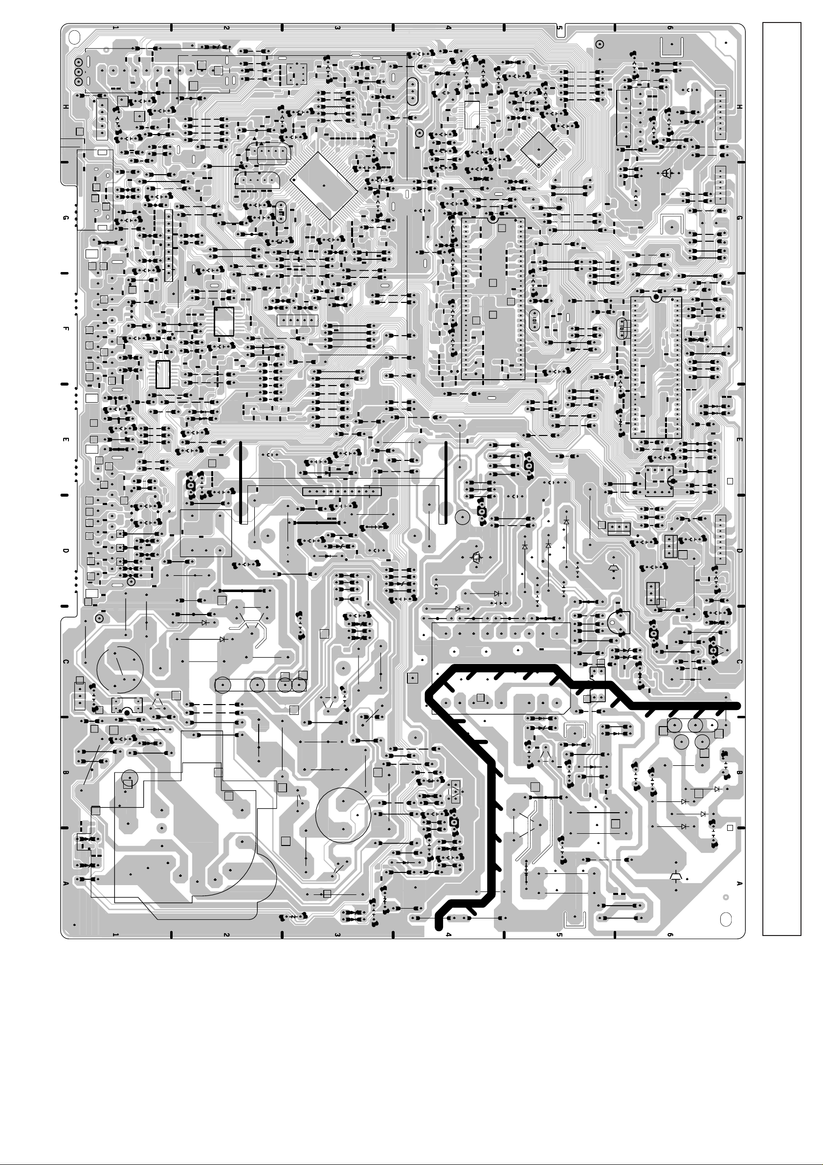
1AA0B10E662G0 ASSY,PWB,MAIN C3YFV
1AA4B10E30800 PWB,MAIN C3AC
C053
CJ180CGQ
TV
C1203
KK0.01
GQ
C1212
CJ82
CGQ
R1201
1/16
GJ
270C
L1202
L2B94
R7KN
C1213
16EM10CD
R1230
1/16GJ
270C
L1206
L2B94
R7KN
C1205
16EM10CD
R480
1/2DJ
2.2B
EU1:
ERA22-04
C1218
CJ82
CGQ
D481
T451-4
2400010
R435
R435-2
2400010
7WK4.7
(I:VC)
R435-1
2400010
145V
TP-B
J30B0250N
C482
250GK
0.1P
2SA1037AKR:
2SA1179NM6P:
TXXKBB001P:
TXXKBB002P:
D1042
1SS133
R1017
1/16GJ
75C
R1050
1/16GJ
75C
R1034
1/16GJ
10KC
D1025
UDZS10BG
D1026
UDZS10BG
D1052
UDZS10BG
T451
L40B10000
T451-6
2400010
6
T451-5
2400010
5
T451-3
2400010
3
4
T451-1
2400030
1
T451-10
2400010
10 7
T451-2
2400030
2
C437
250GJ0.47:
250GJ0.47PA
R450
15K
R455
R454
DJ39K
DJ56K
R481
DJ
270K
R482
8.2K
D482
1SS133
TECT
R1043
1/16GJ
4.7KC
1SS133
TXXKBB003P
R1003
75
D1002
UDZS10BG
+5V
Q1044
UDZS10BG
R453
1K
PRO
D445
1SS355
D1041
Q1042
L1004
UDZS10BG
UDZS10BG
UDZS10BG
C1015
16EM10CD
KK1000GQ
R1044
1/16GJ
4.7KC
Q1043
UDZS10BG
D1047
C1027
16EM10CD
KK1000GQ
C1029
16EM10CD
KK1000GQ
C1042
16EM10CD
KK1000GQ
C1043
16EM10CD
KK1000GQ
C450
100PM
2.2X
+5V
J
D1003
UDZS10BG
D1007
D1008
D1010
L1010
L2B9
100KN
C1010
CJ100
CGQ
C1012
CJ100
CGQ
C1014
C1017
16EM10CD
R1046
1/16GJ
22KC
R1047
100
D1043
UDZS10BG
D1046
UDZS10BG
C1024
CJ100
CGQ
C1026
C1028
C1044
C1045
T451-11
2400010
11
T451-7
2400010
R447
1/16GJ
4.7KC
Q1041
2SC2412KR:
2SC2812NL6P:
TXXKBB004P:
TXXKBB005P:
TXXKBB006P
R1042
100
L1011
L2B9
100KN
L1012
L2B9
100KN
C1016
KK1000GQ
D1044
L1020
L2B9
100KN
C1021
CJ100
CGQ
L1021
L2B9
100KN
L1022
L2B9
100KN
L1023
L2B9
100KN
L1018
L2B9
100KN
100KN
R451
2SJ2.7
C451
100PM
2.2X
MTZJ8.2B
VIDEO OUT
R1002
1/16GJ
75C
R1005
1/16GJ
75C
R1009
1/16GJ
75C
R1011
1/16GJ
75C
R1012
1/16GJ
2.2KC
C1034
CJ100
CGQ
R1021
2.2K
R1022
1/16GJ
560C
R1023
1/16GJ
560C
L1019
L2B9
R1032
1/16GJ
560C
D446
R1013
1/16GJ
2.2KC
R1014
1/16GJ
560C
L1013
L2B9
100KN
UDZS10BG
R1048
1/16GJ
75C
R1019
1/16GJ
75C
R1049
1/16GJ
75C
R1020
2.2K
R1001
39K
R1031
1/16GJ
560C
R1041
1/16GJ
22KC
1/16GJ
75C
D1021
R
R1007
G
B
R1016
39K
L1017
ZZ0122
R448
DJ330
L1003
ZZ0122
R1015
1/16GJ
560C
R1018
75
C IN
L-OUT
KQ
J10EA030N
J30B0250N
D442
1SS355
C445
EM10CD
R
G
B
R-OUT
KSC
21
19
17
15
13
11
9
7
5
3
1
21
19
17
15
13
11
9
7
5
3
1
J12B2821N
3
2
1
20
18
16
14
12
10
8
6
4
2
K1001
J1EK1745B
:J11B0490N
20
18
16
14
12
10
8
6
4
2
K1002
J1EK1745B
:J11B0490N
K1003
3
TO
SOCKET
2
K7Q
1
HV
SCREEN
VIDEO IN
L-IN
R-IN
DY1
X
Page 5

MAIN BOARD
BLOCK DIAGRAM (OUTLINE)
Part No. SKP20370 C3YFV (SHEET 3-3)
C607
R602
R637
IC643
KA KH
IC642
IC801
IC803
IC001
Q613
Q641
T451
T611
Q432
VR641
IC641
IC501
TP-B
C502
C501
IC3451
KP
IC201
T131
X131
X132
SPEAKER
SP902
SP901
D603-D606
C607
SW901
AC
Q613
Q611
8/10
IC001
AUDIO-OUT
<TDA7263M>
T611
CONVERTER
5
8
2
3
D615
15
18
11
14
13
10
1 5
12
-27V
Q666
Q661
Q642
L462
25V
Q651
Q641
KEY SW
I2C BUS
CONTROL
IC803
MEMORY
5V
IC641
IC642
IC643
27V
145V
Reg.
Q643
RC RECEIVER
SDA
SCL
5V
D646
9V
5V-1
Q645
T431
K1002
A1901
RC-IN
KEY-IN
SDA
SCL
PROTECT
D641
D647
D637
Q685
Q686
IC801
CPU
1
8
19
20
21
11
Q682
MUTE
45
BLK
18
R
17
G
16
B
15
H-BLANK
4
34
33
53
54
SCREEN
POWER
WIDTH
CONTROL
D441
IC501
V-OUTPUT
<LA7846>
IC1201
A101
K1001
TP-A
K1003
KCPA
Video-IN
R/G/B-IN
Video/
R/G/B-IN
B
R
PICTURE
G
AERIAL
SCL
SDA
C-IN
Y-IN
19
C-IN
TUBE
19
SCART SC1
20
11/7/15
15
20
SCART SC2
15
7/11/15
K1001
K1002
IC3451
71
26
27
20
21
22
23
33
47
39
R
12
G
13
B
14
R/G/B-OUT
NICAM/
STEREO
IF-IN
80
79
SIF-IN
75
76
IF/VIDEO/CHROMA/DEF
X131
<TB1251>
IC201
54
48
46
58
61
51/53
57
56
55
Video-Out
C-IN
Y-IN
M-OUT
R
G
B
T451 FLYBACK
CRT
HEATER
A101
TUNER
C-OUT
13
12
1/3/13
2/5/12
IF
X132
AV-VIDEO-SW <LA7954>
IC1201
9816
Video/Y-Out
4
14
15
IC1401
RGB-SW
<TC4053BF>
Q701
Q711
Q721
60 61
5
SDA
Q462
Q461
12
SIF-OUT
SCL
SDA
EW-OUT
V-OUT
H-OUT
L461
L462
4
SCL
6
3
Q432
H-OUTPUT
Q431
H.V
D.Y
200V
FOCUS/SCREEN
Page 6

OPTION SETTING
[After replacing the Memory IC (IC803)]
The memory IC, IC803, stores the option data of TV set and service adjustments data for each circuit, therefore,
when the memory IC is replaced, it should be performed following setting and “SERVICE ADJUSTMENT” on next
page.
To enter to the Option Mode
+ Press and hold the F/OK button on the remote control and P▼ button on the front panel of the TV. The option
window will appear on the screen.
OPTION
ON-TIMER ON
SORT MODE SORTING
P&P ON
WEL. TEXT ON
COMB FILTER OFF
BBE OFF
AUTO VOLUME OFF
HEADPHONE OFF
COUNTRY BG/DK/I/LL'
WIDE ON
ADJUST : EXIT : RECALL
OPTION MODE FOR CE32WN5F-C-04
To set the option mode
+ Highlight the desired option item by using the P▲ or P▼ button .
+ To switch the option mode, use the Volume - (LEFT) or Volume + (RIGHT) button.
+ The data which is set in the option mode is stored into the memory IC automatically.
Following table shows the available option items and default setting mode.
Option Mode Mode Description & Note
ON-TIMER ON or OFF On-timer available, default “ON”
SORT MODE SORTING or Tuning mode, default “SORTING”
TUNING
P & P ON or OFF Plug & Play mode, default “ON”
WEL. TEXT ON or OFF Display message when first set up, default “ON”
COMB FILTER OFF or ON For factory use, default “OFF”
BBE ON or OFF BBE sound mode, default “OFF”
AUTO VOLUME ON or OFF Default “OFF”
HEADPHONE ON or OFF Headphone control , default “OFF”
COUNTRY UK, IRE TV system, default “UK”
BG/DK / I / LL’
WIDE ON or OFF Wide mode, default ON
Exit from the Service Mode
+ Press the RECALL button.
?
SERVICE ADJUSTMENTS
Note: Some items of the service adjustments for this chassis are controlled by the CPU, IC801, and the
adjustments are carried out by using the RC handset.
[After replacing the Memory IC (IC803)]
The memory IC, IC803, stores the service adjustments data for each circuit, therefore, when the memory IC is
replaced, it should be programmed by using “OPTION SETTING” on previous page and the following adjustments.
ADJUSTABLE SERVICE ADJUSTMENT
REGULAR
Item No. OSD Description
1 AGC AGCAdjustment
2 -- Cut-Off Drive Adjustment
3 GR Y G-Drive Adjustment (white balance)
4 GR Y B-Drive Adjustment (white balance)
5 CTR Contrast Adjustment (use factory setting)(for factory use)
6 -- Screen Adjustment mode
8 OSD OSD Positioning Adjustment
IMAGE
ADJUSTMENTS
IMPORTANT NOTICE
Do not attempt to adjust the following service adjustments except when adjustments are required in servicing
otherwise it may cause loss of performance and product safety.
ADJUSTMENT
+ B VOLTAGE
1. Receive white raster pattern.
2. Set controls to normal.
3. Connect digital voltmetre to test point TP-B and GND.
4. Adjust voltage to 145 ±0.5V by using VR641.
ADJUSTMENT
AGC ADJUSTMENT
1. Input and tune an RF signal which is UHF to the clearest station.
2. Connect digital voltmetre to test point TP-A and GND.
4. Enter to the service mode and select mode “REGU-
LAR”, and select item no.1 “REGULAR 1, AGC”.
5. Press the LEVEL+ or LEVEL - button to adjust volt-
age to be 3.2Vdc.
FOCUS ADJUSTMENT
By using FOCUS VR, adjust focus control for well
defined scanning lines.
GREY SCALE ADJUSTMENT
SCREEN
ADJUSTMENT
1. Receive black & white pattern.
2. Enter to the service mode and select mode “REGU-
LAR”, and select item no. 2 “REGULAR 2, CUT”. The
horizontal line will appear on the screen.
3. Set the SCREEN VR for one colour to be just visible.
4. Using the numeric buttons shown set each colour to
minimum by decreasing to the point where any further
decrease resets the adjustment to maximum value.
ADJUSTMENT
BIAS
5. By using the buttons 1, 2, 4, 5, 7, 8 on the remote
control, adjust the line to be white.
The key allocation is as follows;
Button No. Operation
1 Increase Red
2 Decrease Red
4 Increase Green
5 Decrease Green
7 Increase Blue
8 Decrease Blue
CORNER ADJUSTMENT
1. Receive cross hatch pattern and set screen mode to
“FULL”.
2. Enter to the service mode and select mode “IMAGE”,
and select item no. 11 “IMAGE 11.P ECT” for top corner adjustment OR item no. 12 “IMAGE 12.P ECB for
bottom corner adjustment.
3. Press the LEVEL+ or LEVEL - button to correct the
distortion of the vertical line around the corners.
HORIZONTAL ADJUSTMENT
HORIZONTAL CENTRING ADJUSTMENT
1. Receive circular pattern and set screen mode to
“FULL”.
2. Enter to the service mode and select mode “IMAGE”,
and select item no. 2 “IMAGE 2.P H-P”.
3. Press the LEVEL+ or LEVEL - button to adjust the
horizontal centre.
HORIZONTAL WIDTH ADJUSTMENT
1. Receive circular pattern and set screen mode to
“FULL”.
2. Enter to the service mode and select mode “IMAGE”,
and select item 6 “IMAGE 6.P H-S”.
3. Press the LEVEL+ or LEVEL - button to adjust the
horizontal width.
DRIVE
6. Select item no.3 “REGULAR 3, GRY” (G-Drive) or 4
“REGULAR 4, GRY” (B-Drive) and adjust both initially
to 40.
7. Change data value of each item by using LEVEL + or
LEVEL - button to obtain the proper white balance.
PCC ADJUSTMENT
PCC
ADJUSTMENT
1. Receive cross hatch pattern and set screen mode to
“FULL”.
2. Enter to the service mode and select mode “IMAGE”,
and select item no. 7 “IMAGE 7.P E-P”.
3. Press the LEVEL+ or LEVEL - button to adjust the
vertical line to be straight.
TRAPEZOID
1. Receive cross hatch pattern and set screen mode to
2. Enter to the service mode and select mode “IMAGE”,
3. Press the LEVEL+ or LEVEL - button to correct the
ADJUSTMENT
“FULL”.
and select item no. 8 “IMAGE 8.P E-T”.
trapezum distortion of the vertical line.
VERTICAL ADJUSTMENT
CENTRING ADJUSTMENT
VERTICAL
1. Receive circular pattern and set screen mode to
“FULL”.
2. Enter to the service mode and select mode “IMAGE”,
and select item no. 1 “IMAGE1.P V-C”.
.3 Press the LEVEL+ or LEVEL - button to adjust the
vertical centre.
VERTICAL HEIGHT ADJUSTMENT
1. Receive circular pattern and set screen mode to
“FULL”.
2. Enter to the service mode and select mode “IMAGE”,
and select item no. 5 “IMAGE 5.P V-A.
3. Press the LEVEL+ or LEVEL - button to adjust the
vertical height.
Item No. OSD Description
1 PV-C P Vertical Position Adjustment
2 PH-P P Horizontal Position Adjustment
3 PV-L P Vertical Linearity Adjustment
4 PVSC P Vertical S-Correction Adjustment
5 PV-A P Vertical Size Adjustment
6 PH-S P Horizontal Size Adjustment
7 PE-P P Pin Cushion Adjustment
8 PE-T P Trapezoid Distortion Adjustment
11 P ECT P Top Corner Correction Adjustment
12 P ECB P Bottom Corner Correction Adjustment
13 P HPA P Parallelogram Distortion Adjustment
IMPORTANT NOTICE
Do not attempt to adjust service adjustments not listed on the above otherwise it may cause
loss of performance and product safety.
To enter to the Service Mode
+ Press and hold the GREEN button on the remote control and then press the P▼ button inside of the door. Press
the P▼ button to highlight the mode required (Regular, Image, others and TB12**). Then press the F/OK button to
select the mode.
The available adjustment items are as follows;
Image : This can be adjusted for picture images/shapes.
Regular : This can be adjusted for the service adjustment.
other : This is for factory setting. DO NOT ADJUST.
TB1251 : This is for the factory setting. DO NOT
To select the mode and service item and change data value
+ Highlight the desired adjustment mode by using the P▲ or P▼ button and then press the F/OK button.
+ To select the adjustment item, use the P▲ or P▼ button.
+ To change the service data, use the Volume -(LEFT) or Volume + (RIGHT) button.
+ The data which is set in the service mode is stored into the memory IC automatically.
REGULAR mode
REGULAR
1, AGC 38
Adjustment No.
and Item name
Adjustment Data
ADJUST
.
Adjustment No.
and Item name
IMAGE mode
IMAGE
1. P V-P 1F
Adjustment Data
Exit from the Service Mode
+ Press the RECALL button or turn off the TV set by using the Mains switch.
?
INITIALISATION OF MEMORY IC
To initialise the memory IC (IC803), press and hold the NORMAL button on the remote control, then press
the P▼ button on the front panel of the TV set and then turn the Mains switch Off and On. The initialisation is now
completed.
When initialised the memory IC and all of the setting data (option data and service adjustment data) stored in the IC
are reset to the default value. It is necessary to set the option settings and readjust the service adjustments listed on
page 6 and to re-tune all the channels.
OSD POSITIONING ADJUSTMENT
1. Receive circular pattern and set screen mode to
“FULL”.
HIGH-VOLTAGE CONFIRMATION
1. Receive circular pattern and set screen mode to
“FULL”.
2. Set controls for brightness and contrast to maximum.
3. Connect high-voltage meter to the anode of CRT and
GND.
4. Confirm that voltage is:
26.5±1.0kV,1.1mA for 24” Wide model
29.5±1.0kV,1.15mA for 28” Wide model.
30.5±1.0kV,1.4mA for 32” Wide model.
29.5±1.0kV,1.35mA for 28” Flat wide model.
30.5±1.0kV,1.45mA for 32” Flat wide model.
2. Enter to the service mode and select mode “REGULAR”, and select item no. 8 “REGULAR 8 OSD”. The
OSD test bar will appear on the top of screen.
3. Press the LEVEL+ or LEVEL - button to adjust prop-
er OSD positioning.
❚❚❚❚❚❚❚❚❚❚❚❚❚❚❚❚❚❚❚❚
CPU PORT FUNCTIONS
Pin No. Function Name Function IN/OUT
1 RC IN RC Signal Input IN
2 RESET Reset Input IN
3 50/60 50/60Hz output 50Hz:H OUT
4 H-BLK H-Blank (on/off?) OUT
5 V-BLK -6 AV-SW2 Option SW2 -7 AV-SW1 Option SW1 -8 KEY IN Key switch signal input IN
9 H-P
10 RELAY To operate degauss circuit OUT
11 PROTECT Power failure detect input “L” error IN
12 HP-MUTE OUT
13 BBE OUT
14 ? OUT
15 B-OUT Blue output OUT
16 G-OUT Green output OUT
17 R-OUT Red output OUT
18 FB-OUT Fast Blanking output OUT
19 SDA SDA IN/OUT
20 SCL SCL OUT
21 VDD Power -22 Not used -23 Not used -24 Not used -25 AVDD3 Analogue VDD of PLL -26 TEST0 Test -27 MCFM Test -28 -29 TXCF Analogue pin for Teletext slicerline PLL -30 -31 AVDD2 Analogue power supply -32 Not used -33 Video input (H.F) IN
34 Video input (L.F.) IN
35 Not used -36 Not used -37 Not used -38 PXFM Analogue pin for the Display Pixel Frequency Multiplier -39 VDDA -40 H-SYNC Horizontal Sync. Input IN
41 V-SYNC Vertical Sync. Input IN
42 ACK Answer for status OUT
43 STATUS Request for BUS open IN
44 INGNOR Not Used -45 MUTE Sound Mute on/off switch OUT
46 L/L’ Not used OUT
47 LED Led drive OUT
48 S-VHS-SW Not used -49 H-PHASE Not used -50 OSC Clock oscillator
51 OSC Clock oscillator IN
52 AGC Auto gain control IN
53 P-TTAR1 Pittari switch (Natural wide) OUT
54 POWER & RL Power & relay On/Off control OUT
55 8PIN (SC2) AV2 Scart function input IN
56 8PIN (SC1) AV1 Scart function input IN
IN
 Loading...