

Page 1
Part No. SKSM0821 N2RL SEPTEMBER 2005
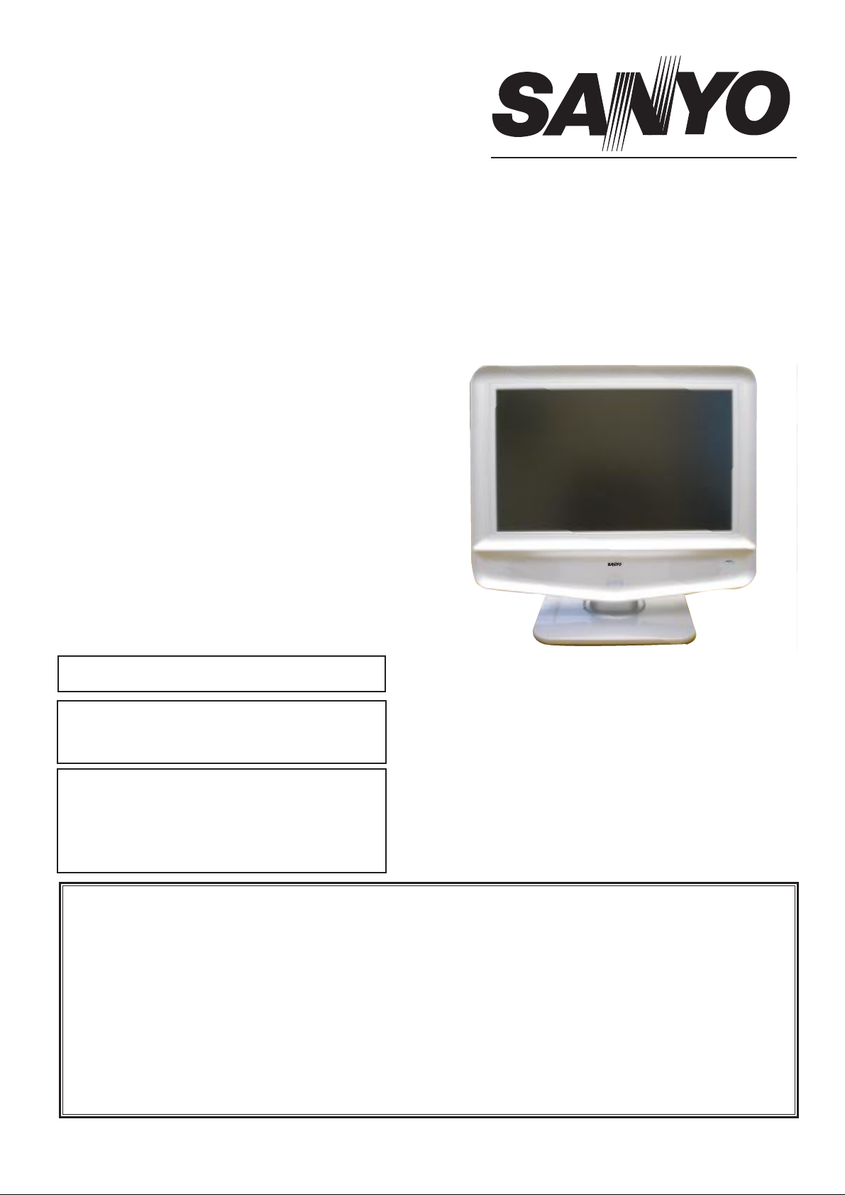
Colour Television
Service Manual
Model CE23LC4-C
Service Ref. No. CE23LC4-C-00
PRODUCT CODE: 111374310
ORIGINAL VERSION:Chassis No.UK1-A
Give complete "SERVICE REF. NO." for parts
order or servicing, it is shown on the rating sheet
on the cabinet back of the TV set.
Note
This TV receiver will not work properly in foreign
countries where the television transmission
system and power source differ from the design
specifications. Refer to the specifications for the
design specifications
CE23LC4-C
Contents
Safety precautions/Specifications ..................................................................................................................2
Option settings............................................................................................................................................3~4
IC descriptions............................................................................................................................................5~6
Service Data ..............................................................................................................................................7~8
Block Diagram ................................................................................................................................................9
IC Block Diagrams........................................................................................................................................................................10~14
CPU Functions ........................................................................................................................................15~19
Cabinet Parts List ........................................................................................................................................20
Cabinet Disassembly....................................................................................................................................21
Pin description of semiconductors................................................................................................................22
Part Description and reading of schematic diagram ....................................................................................23
Electric Parts List....................................................................................................................................24~30
Please use Schematic Diagram SKP20552
inserted with this Service Manual.
Page 2
-2-
N2RL
SAFETY PRECAUTION
X-RADIATION PRECAUTION
The primary source of X-RADIATION in the television receiver is the picture tube. The picture tube is specially
constructed to limit X-RADIATION emissions. For continued X-RADIATION protection, the replacement tube
must be the same type as the original including suffix letter. Excessive high voltage may produce potentially
hazardous X-RADIATION. To avoid such hazards, the high voltage must be maintained within specified limit.
Refer to this service manual, high voltage adjustment for specific high voltage limit. If high voltage exceeds
specified limits, take necessary corrective action. Carefully follow the instructions for +B1 volt power supply
adjustment, and high voltage adjustment to maintain the high voltage within the specified limits.
PRODUCT SAFETY NOTICE
SPECIFICATIONS
Product safety should be considered when a component replacement is made in any area of a receiver.
Components indicated by mark in the parts list and the schematic diagram designate components in which
safety can be of special significance. It is particularly recommended that only parts designated on the parts list in
this manual be used for component replacement designated by mark . No deviations from resistance wattage
or voltage ratings may be made for replacement items designated by mark .
1: An isolation transformer should be connected in the
power line between the receiver and the AC line
when a service is performed on the primary of the
converter transformer of the set.
2: Comply with all caution and safety-related notes
provided on the cabinet back, inside the cabinet, on
the chassis or the picture tube.
3: When replacing a chassis in the cabinet, always be
certain that all the protective devices are installed
properly, such as, control knobs, adjustment covers
or shields, barriers, isolation resistor-capacitor networks
etc. Before returning any television to the customer,
the service technician must be sure that it is completely
safe to operate without danger of electrical shock.
Power source AC 220~240V, 50Hz
Television system System I
Colour system PAL/NTSC4.43 (PAL/NTSC4.43/NTSC3.58 IN AV MODE)
Receiving channel UHF: #21~69
Aerial input impedance 75ohm
Rear AV terminal
AV1: CENELEC standard
INPUT: Composite video, RGB and Audio L/R
OUTPUT: TV-output with composite video and audio L/R
AV2: CENELEC standard
INPUT: Composite video, RGB, S-VHS and Audio L/R
OUTPUT: Monitor output with composite video and Audio L/R
Front AVterminal
AV3: RCA jacks
INPUT: Composite video and Audio L/R
Sound output(Music) 12 x 2
Dimensions (WxHxD) 580 x 480 x 257mm
Weight 8.4 Kg
!
!
!
Important recycling information.
Your SANYO product is designed and manufactured with high quality
materials and components which can be recycled and reused.
This symbol means that electrical and electronic equipment, at their
end-of-life, should be disposed of separately from your household
waste.
Please dispose of this equipment at your local community waste collection / recycling centre.
In the European Union there are separate collection systems for used electrical and electronic
products.
Please help us to conserve the environment we live in!
Note: This symbol mar k and recycle system are applied only to EU countries and are not applied
to other countries of the world.
Page 3
-3-
N2RL
OPTION SETTING
To enter to the Option Mode
+ Press and hold the F/OK button on the remote control and P▼ button on the front panel of the TV. The option win-
dow will appear on the screen.
To set the Option Mode
+ Highlight the desired option item by using the P▲ or P▼ button .
+ To switch the option mode, use the Volume - (LEFT) or Volume + (RIGHT) button.
+ The data which is set in the option mode is stored into the memory IC automatically.
The following table shows the available option items and default setting mode.
Exit from the Option Mode
+ Press the MENU button.
Option Mode Mode Description & Note
OSD H-POS Set value to 6
COUNTRY EU or UK Country default “EU”
SORT MODE Sort mode, default “Sorting”
PLUG & PLAY ON or OFF Plug & Play mode, default “ON”
WELCOME TEXT ON or OFF Welcome Text default “ON”
SURROUND ON or OFF Surround sound default “ON”
BASS FEATURE Bass Feature default “BBE+Bass Exp”
AVL ON or OFF AVL mode, default “OFF”
AV3 ON or OFF AV3 mode, default “ON”
COLOUR SYSTEM ON or OFF Colour system, default “OFF”
AFC ON or OFF AFC mode, default “ON”
PROGRAM NAME ON or OFF Program name default “OFF”
TEXT NO SIGNAL ON or OFF Disables Text when no signal, default “ON”
BLUE BACK ON or OFF Blue Black mode, default “OFF”
DIGITAL MODE ON or OFF Digital mode, default “OFF”
SCART Set value to 2
OPTION MODE FOR CE23LC4-C-00
Option
OSD H-Pos 6
Country EU
Sort Mode SORTING
Plug & Play ON
Welcome Text ON
Surround ON
Bass Feature BBE+Bass Exp
AVL OFF
AV3 ON
Colour System OFF
AFC OFF
Program Name ON
Text no signal ON
Blue Back OFF
Digital Mode OFF
Scart 2
i
Page 4

-4-
N2RL
OPTION SETTINGS
Analogue Settings for All UK1A N2R* and N2S*
38 38 38 25 25
50 50 50 50 50
30 30 30 33 33
N2RJ N2RK N2RL N2SJ N2SL
PICTURE
Brightness
35 35 35 35 35
Contrast
Colour
Sharpness
47 47 47 30 30
63 63 63 63 63
35 35 35 40 40
40 40 40 40 40
Brightness
Contrast
Colour
Sharpness
31 31 31 25 25
32 32 32 35 35
30 30 30 35 35
32 32 32 35 35
Brightness
Contrast
Colour
Sharpness
00000
Off Off Off Off Off
Dyn skin tone
10 10 10 10 10
Max Max Max Max Max
TXT Brightness
SOUND
Volume
Balance
00000
00000
Off Off Off Off Off
Off Off Off Off Off
Normal Normal Normal Normal Normal
Bass
Treble
Sound Preset
BBE
Surround
OPTION
OSD H-Pos 66666
Country EU UK EU EU EU
Sort Mode Sorting Sorting Sorting Sorting Sorting
Plug+Play On On On On On
Welcome Txt On On On On On
Surround On On On On On
Bass Feature BBE+Bass Exp BBE+Bass Exp BBE+Bass Exp BBE+Bass Exp BBE+Bass Exp
AVL Off Off Off Off Off
AV3 OnOnOnOnOn
Colour System Off Off Off Off Off
AFC Off Off Off Off Off
Program Name On On On On On
TXT no signal On On On On On
Blue Back Off Off Off Off Off
Digital Mode Off On Off Off Off
Scart 22222
Page 5

-5-
N2RL
IC Descriptions for UK1A
IC001
This is an LA42052 which is the audio amplifier for the set. It has left and right inputs from the LOC and left and right
outputs to the speakers and headphone socket. It also has mute and standby functions which are activated by the
LOC as appropriate.
IC1101 (monitor sets only)
This is a switching IC, NJM2233BM, which allows the sync signal input on monitor sets to be switched between pin
20 of SCART 1 (conventional & ALBOS) and pin 14 of SCART 1 (SIS signal). The IC takes a 5V supply and is
switched by the control line SC2_8, which is normally used for SCART 2 pin 8 signalling but is adapted fro the moni-
tor sets.
IC1205
This a ROHM BA7603F triple video switch which allows the RGB input to be switched between SCART 1 and
SCART 2. The switch is controlled by the RGB_SW line from the IC.
IC2001
This is a picture improvement chip, Philips TDA9178, which takes a YUV input from the LOC and carries out vector
processing of luminance and colour to improve overall picture quality and reduce noise. The IC requires an 8V
power supply and is also connected to the I2C bus.
IC201
This is the Philips LOC 1 chip which is the main system processor. It consists of three ICs encapsulated in one BGA
package with 388 balls. The “Cosmic” and “Picasso” chips carry out analogue and digital processing respectively,
and together from the UOC III which is used in many other sets. These are complemented by the Lithium IC which
carries out digital processing and scaling functions.
The IC requires 5V, 3.3V and 1.8V for correct operation – although only 5V and 3.3V are required in “standby”
mode. Full descriptions of all port functions are given elsewhere in this manual.
IC1221(digital only)
This is a ROHM BA7609F triple video switch which allows audio and video from the digital system to be output to
the SCART 2 socket for recording. The IC is controlled by the REC_CTL signal from the MCU IC860.
IC4001
This is a SST SST39VF020 CMOS multi-purpose flash with a capacity of 2Mbits. It is connected to the LOC using
address lines, data input/output, write enable and control lines. The flash IC is powered by the 3V3 SW supply.
IC4002
This is a ROHM BD5260G open drain voltage detector IC which works in conjunction with the backlight enable line
BL_EN. It takes input from the main power and the 5V CPU line.
IC6600
This is a chopper regulator, Sharp PQ1CY series, which provides the power for the LCD panel – 3.3V for 15” and
20”, 5V for 17” and 23”. The regulator is switched on at power up via the control line POWER 1 and transistor
Q6600. The power is switched to the panel, also by POWER 1, via the FET switch Q1600.
IC6602
This is a Sharp PQ1CZ series chopper regulator which provides the 14V supply for the audio IC. It is switched by
the control line POWER 1 from the LOC.
Page 6

-6-
N2RL
IC Descriptions for UK1A (continued)
IC6603(digital only)
This is a Sharp PQ1CZ series chopper regulator which provides the 6V supply for the digital module, hence it is only
present on digital sets. The regulator is switched by the POWER 1 control line from the LOC.
IC6604
This is a linear voltage regulator providing in this case 8V to supply the picture improvement IC IC2001. The regulator is switched by the control line POWER 1.
IC6605
This is a chopper regulator, Sharp PQ1CY series, which provides 6V. This voltage is clamped by a diode after the
regulator to produce 5V CPU. This voltage is passed to IC 6606.
IC6606
This is a linear voltage regulator, ROHM BA05SFP, which takes the 6V from IC6605 as an input and produces 5V
SW. This regulator is controlled by the POWER 1 control line from the LOC.
IC6607
This is a linear voltage regulator which takes the 6V from IC6605 and produces 3V3 STB used by the LOC in standby mode.
IC6608
This is a ROHM BA00BC0WFP linear regulator which converts the 6V from IC6605 to the 1V8 use by the LOC
when the set is powered on. This regulator is controlled by the POWER 1 control line.
IC6642
This is also a ROHM linear regulator which takes the 5V SW from IC6606 as an input and produces 3V3 SW used
by various parts of the circuit.
IC701 (20” LCD only)
This is a THine THC63LVDF84B LCD panel interface which converts 4 LVDS data streams from the LOC into 28bits
of RGB data and a clock to send to the panel. Currently this IC is only required on 20” LCD sets where the panel
requires data in RGB form rather than LVDS.
The IC requires a 3V3 power supply on several pins.
IC801
This is the non-volatile memory(NVM) IC which contains data settings for the LOC and stored user data such as picture settings and programs. It also contains data relating to the LCD panel type and data requirements. It is a 24C64
64K EEPROM arranged as 8192 x 8bits. It uses the 3V3 STB power supply and is connected to the LOC via the
12C bus.
IC860(digital only)
This is a Renesas RSF21162SP microprocessor which acts as a controller for the digital module via the I2C bus and
the D/A_CTL and REC_CTL line to IC1251 and IC1221. This IC has a small amount of memory which contains the
ICs program, this is programmed separately from the LOC program via the KSUB socket.
IC861(digital only)
This is a ROHM BD4828G CMOS voltage detector which controls the reset line to the IC860 microprocessor.
Page 7

-7-
N2RL
To enter to the Service Mode
+ Press and hold the GREEN button on the remote control and then press the P▼ button on the cabinet.
To select the service item and change data value
+ To select the adjustment item, use the P▲ or P▼ button.
+ To change the service data, use the Volume -(LEFT) or Volume + (RIGHT) button.
+ The data which is set in the service mode is stored into the memory IC automatically.
EXAMPLE: 000 GTV 4.0 E4.17
ITEM NO SECTION VALUE
ITEM
Exit from the Service Mode
+ Press the MENU button or turn off the TV set by using the Mains switch.
Page 8
-8-
N2SL
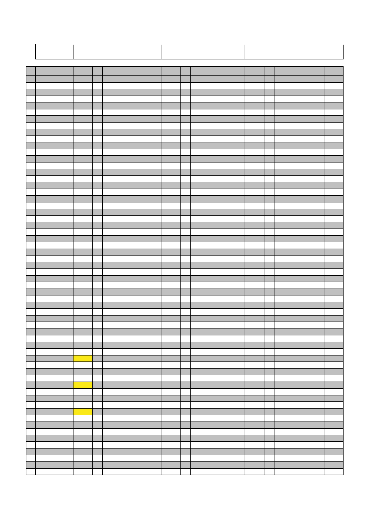
SERVICE DATA
Software ver E417Model: N2RL NVM file: N2RL_070405_5C4E
items marked have changed from previous NVM data
# item value # item value # item value # item value
0 Soft. Version E417 60 MUS 0 120 9178 CTI-RF 1 180 CHSE 2
1 Init TV 0 61
2 ISP Mode 0 62 CB 0 122 9178 SP-RF 32 182 NUEL 200
3 Sedna version 10601 63 CB PF PAL 0 123 9178 CR-RF 32 183 DSG 1
4 PWT 0 64 CB AV NT 0 124 9178 LW-RF 32 184 FMWS 1
DCXO
5
6 DCXO Auto 0 66 FCO 0 126 PeakFrq-RF 3 186 PA-BA-MU 48
7 WSS 1 67 PeakFreqPAL443 3 127 SCA Lit H Flt-RF 30 187 PA-TR-MU 45
8 WPR 20 68 PeakFreqPALM 3 128 SCA Lit V Flt-RF 27 188 PA-BA-TK 28
9 WPG 20 69 PeakFreqPALN 3 129 9178 CFS-AV 1 189 PA-TR-TK 40
10 WPB 20 70 PeakFreqNTSC443 3 130 9178 VDC-AV 1 190 PA-BA-NR 32
11 BLOR 20 71 PeakFreqNTSCM 3 131 9178 CDS-AV 0 191 PA-TR-NR 32
12 BLOG 20 72 PeakFreqSECAM 3 132 9178 CTI-AV 1 192 BEEP-VOL 35
13 WPR-SECAM 0 73 PeakFreqAV 3 133 9178 PK-AV 35 193 BEEP-FRQ 4
14 WPG-SECAM 0 74 Tint Def 32 134 9178 SP-AV 32 194 AGC Speed 1
15 WPB-SECAM 0 75 Tint NT 0 135 9178 CR-AV 20 195 AGC Take over 27
16 BLOR-SECAM 0 76 Blackstretch 1 136 9178 LW-AV 32 196 OIF 32
17 BLOG-SECAM 0 77 Bluestretch 0 137 UOC COR-AV 3 197 VA 3
18 reserve 32 78 Whitestretch 0 138 UOC PeakFrq-AV 3 198 VAI 0
reserve
19
RGB Bright
20
TXT MIN 6 81 BSD 0 141 HPOS50 425 201 BPB 0
21
22
TXT MID 16 82 AAS 0 142 VPOS50 14 202 BPB2 1
23 TXT MAX 31 83 PeakRatioOvShot 0 143 203 TXT-H-POS 10
24 BR RF PN 245 84 RatioPreAftShot 0 144 204 TXT-H-POSA 24
25 BR AV 245 85 CRA0 0 145 SACR 17 205 TXT-H-POSB 6
26 BR RGB 245 86 DL 0 146 SACG 17 206 OSD-H-POS 6
27 BR S 245 87 Tint NTSC 31 147 SACB 17 207
28 CN RF PN 0 88 OSO 0 148 SAGR 31 208 PGR 45
29 CN AV 0 89 FSL 0 149 SAGG 31 209 PGG 45
30 CN RGB 0 90 HP2 0 150 SAGB 31 210 PGB 45
31 CN S 0 91 SoftClipLevel 0 151 reserve 32 211 BackLight 63
32 SH RF PN 0 92
33 SH AV 0 93
34 SH RGB 0 94 AMS 1 154 reserve 58 214 BL PWMFreq 240
35 SH S 0 95 LDH 1 155 reserve 63 215 GAMMA 32
36 CL RF P 0 96 FHS 0 156 OP AUDIO CON 2 216 BRIFE 55
37 CL AVP 0 97 WLB 1 157 OP DUB DBE 0 217 SATBE 35
38 CL N 0 98 DEM 0 158 AVL-LEV 5 218 CONBE 35
39 CL S 0 99 CD2-0 0 159 AVL-WGT 0 219 PANEL 0
40 CL RGB 0 100 OSP 0 160 AVL-MOD 3 220
41 PV-BR-DY 47 101 WPO 0 161 LOUD-NA 3 221 EGL 0
42 PV-CL-DY 35 102 DSK 1 162 LOUD-CH 0 222 RBL 0
43 PV-CT-DY 63 103 ASK 0 163 BBE-CONT 10 223 FILT BW M 0
44 PV-SH-DY 40 104 WSK 0 164 BBE-PROC 10 224 FILT BW 2
45 PV-BR-ST 38 105 SSK 1 165 OP CLIP 0 225 SCAN TIME 6
46 PV-CL-ST 30 106 DGR 1 166 ADC-AV-L 16 226 Phi 1 2
47 PV-CT-ST 50 107 GGR 0 167 DEC-LEV 16 227 reserve 32
48 PV-SH-ST 35 108 WGR 0 168 MONO-LEV 16 228 reserve 0
49 PV-BR-EC 31 109 SGR 1 169 NIC-LEV 16 229 reserve 32
50 PV-CL-EC 30 110 DBL 0 170 SAP-LEV 16 230 reserve 32
51 PV-CT-EC 32 111 GBL 0 171 E2D 0 231 reserve 63
52 PV-SH-EC 32 112 SBL 0 172 FFI 0 232 reserve 41
53 CLO SECAM 0 113 BON 0 173 MR VOL L 63 233 reserve 58
54 DTR SECAM 1 114 BT5-0 0 174 MR VOL H 4 234 reserve 63
55 YSECAM 12 115 NL5-0 0 175 L HI CUT 26 235 POS chg 30
56 YNTSC 0 116 VG5-0 32 176 ASD SC1 THR 16 236 POS chg no sig 40
57 YPAL 4 117 9178 CFS-RF 1 177 AGN 0 237 zoom or txt 30
58 YAV 4 118 9178 VDC-RF 1 178 OVMADAPT 0 238 dcxo swing 96
59 ACL 0 119 9178 CDS-RF 0 179 OVMTHR 0 239
48 65 BPS 0 125 UOC COR-RF 3 185 CV2 0
32 79 GAM 0 139 SCA Lit H Flt-AV 38 199 SVO 0
29 80 PWL 0 140 SCA Lit V Flt-AV 27 200 GD 1
PWLDAC 8 121 9178 PK-RF 35 181 NLEL 100
CL 0
FO
Picture booster
0 152 reserve 63 212 BL PWMMin 0
1 153 reserve 41 213 BL PWMMax 255
LPG 1
Page 9
-9-
N2RL
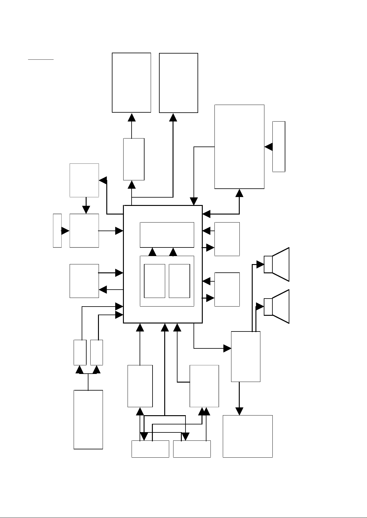
BLOCK DIAGRAM
This is a diagram for all models and therefore differs slightly from the actual block diagram.
i
)
n
Outline
20"
VGA
LCD panel
LCD panel
XGA / WXGA
XGA/WXGA
15", 17", 23"
Digital i
IC860
sub cpu
RSF21162SP
IC1251
BA7603F
YUV switch
IC801
64K NVM
(digital on
(digital on
I2C
TTL
IC701
LVDS to TTL
THC63LVDF84B
IC201 LOC1 TDA15521E
Lithium
Cosmic
LVDS
Picasso
control
IC4001
SST39VF020
IC2001
TDA9178
2Mb flash
power regulators
IC6600 - IC6609, IC 6642
Power Input
RGB
SAW
SAW
video
sound
IC1205
BA7603
RGB switch
tuner
A101
UHF/VHF
SCART 1 SCART 2
sync
video & aud
IC1101
sync switch
NJM2233BM
(monitor only
IC001
LA42052
audio amplifier
side AV
headphone
audio, video
Page 10
-10-
N2SL
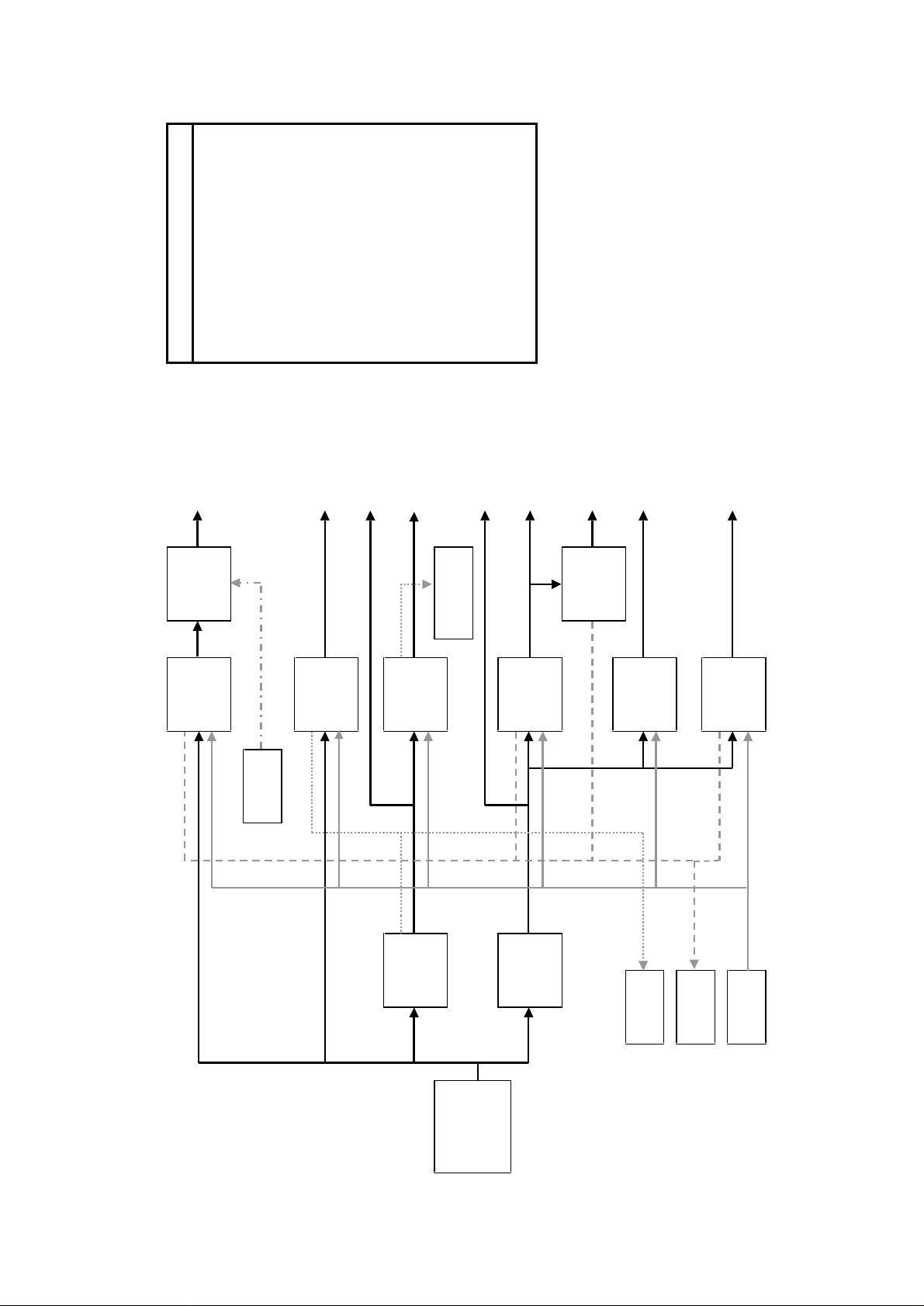
Power Operation
p
e
e
y
p
p
a
g
e
Mains power on, set in "standby", 5V
3V3 STB are available via IC6605 and
When set powers on a HIGH on control
"power 1" switches on regulators to
other voltages required by set.
Power failure at any of these suppli
to the LOC by either "P_FAIL 1" or "P
depending on which supply has failed.
will force the set back into standby.
Once all the voltages are present th
will be enabled by "power 3" via FET
Q1600.
In digital sets the failure of the di
power from IC6603 will be signaled b
DM" to the LOC
ower swIC6600
anel
Q1600
8V
IC6604
UK1A Power - Block Diagram
power 3
from LOC
ital modul
14V audio
6V di
IC6603
5V CPU
to LOC
digi power f
5V SW
3V3 SW
IC6642
3V3 STB
IC6607
1V8 SW
IC6608
IC6602
power input
IC6605 IC6606
to LOC
power fail
power fail
to LOC
power 1
from LOC
Page 11
-11-
N2RL
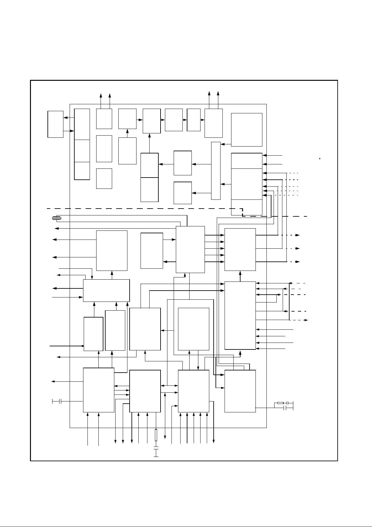
IC201
BLOCK DIAGRAMS
FLASH
FLASH
INTERFACE
µC
SLAVED
4k
SRAM
GPIO
GPIO
GLOBAL
PANEL
PWM
PWM
FONT
CONTROL
PLL
OSD
8k ROM
12k RAM/
MIXER
OVERLAY
SCALER
UP/DOWN
LINE
MEMORY
LUT
OUTPUT
COLOUR
COLOUR
AUTO
UNIT
DITHER
MATRIX
ADJUST
LVDS
(single
or dual
OUTPUT
INTERFACE
INPUT SELECT
pixel)
TEST
IMAGE
2
ANALOG
INTERFACE
LINE
GENERATOR
C
I
(AVI)
PLL
LOC I series
Backend
DDC
PC/HD IN
(RGB H/V sync)
I/Os
LS-OUT
HP-OUT
S
2
I
4 AUDIO IN
1 AUDIO OUT
SSIF
QSSO/AMOUT
REFO
VOLUME
AUDIO CONTROL
A/D
AUDIO
SELECT
SOUND PLL
DEEMPHASIS
AGC
SWITCH
QSS MIXER
QSS SOUND IF
DACs
FEATURES
TREBBLE/BASS
&
D/A
AM
A/D CONVERTER
MULTI-STANDARD
AM DEMODULATOR
PAL/SECAM/NTSC
STEREO DEC.
PLL DEMOD.
VISION IF/AGC/AFC
256K FLASH
REF
DECODER
BASE-BAND DL
VIDEO AMP.
SOUND TRAP
GROUP DELAY
MAIN µC &
DIGITAL
H/V
C
BCR
DECODER
TELETEXT
BL R G
2H/4H
COMB FILTER
Y DELAY ADJ.
Y
VIDEO IDENT.
VIDEO SWITCH
VIDEO FILTERS
RGB MATRIX
TEXT INSERT
BLUE STRETCH
RGB CONTROL
INSERT
R
P
B
RGB/YP
H/V SYNC SEP.
BLACK STRETCH
YUV
/ UV DELAY
YUV INTERFACE
PEAKING
SKIN TONE / U/V TINT
VERTICAL
H-OSC. + PLL
COUNTDOWN
HV
Vi
Ui
Vo Uo Yo Yi
G/Y
BL
B
B/P
R
R/P
RG B
B
B/P
(Cx)
R
R/P
G/Y
(CVBSx/Yx)
SWO1 BL
SIFIN/DVBIN
VIFIN
IFVO/SVO/
AGCOUT
DVBO/FMRO
DVBO/IFVO/
FMRO
CVBSI
YSYNC
CVBS3/Y3
C2/C3
CVBS2/Y2
CVBS4/Y4C4CVBSO/
PIP
Page 12
-12-
N2SL
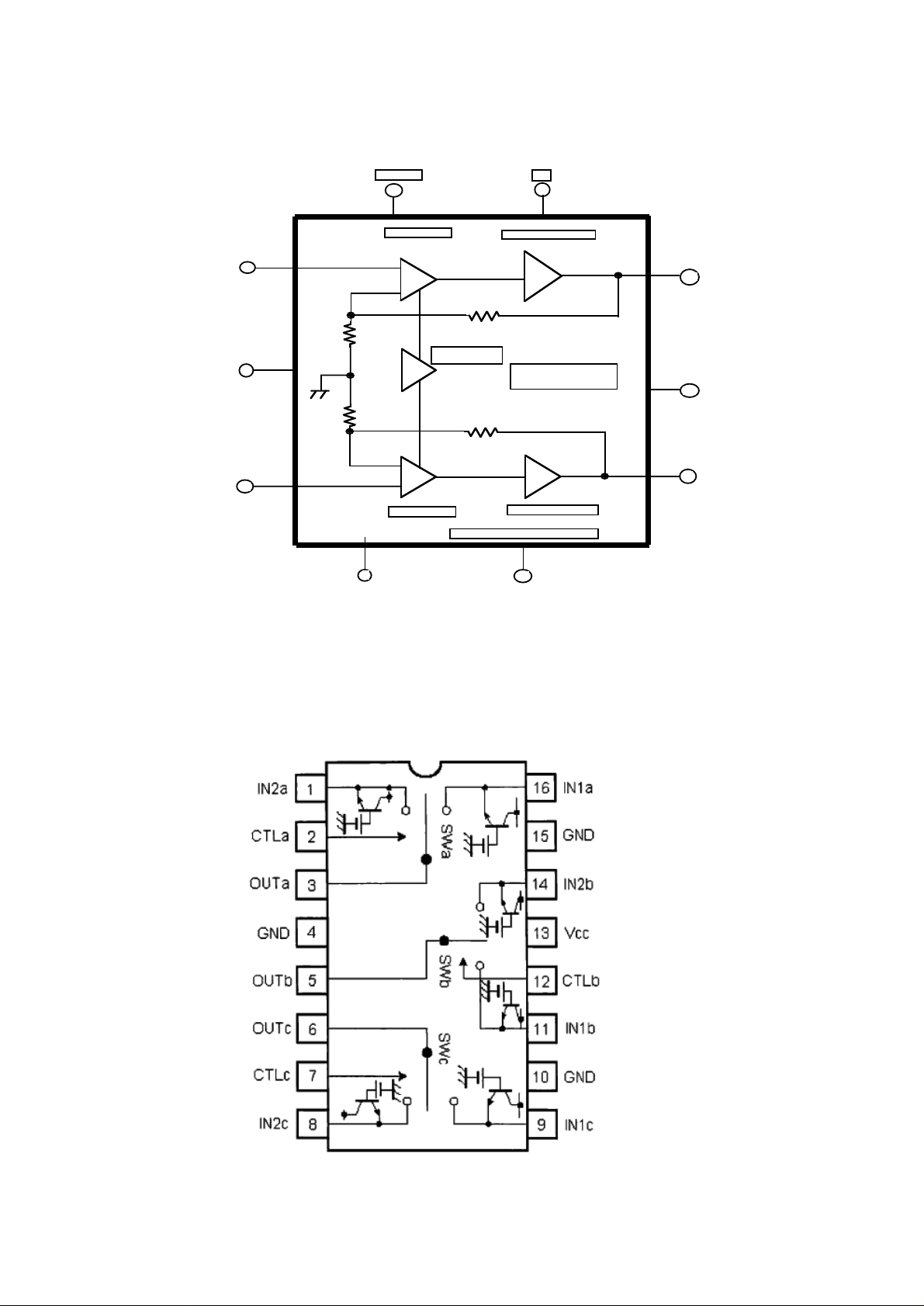
IC BLOCK DIAGRAMS
IC001 LA42052 <Audio Output>
Vcc
IC1205 BA7603F
STAND BY
5 7
INPUT AMPLIFIER
IN 1
REFERENCE
3
IN 2
4
INPUT AMPLIFIER
RIPPLE FILTER
1
RIPPLE FILTER
AMPLIFIER
OUTPUT AMPLIFIER
THERMAL PROTECTION CIRCUIT
OUTPUT AMPLIFIER
POP NOISE PREVENTION BLOCK
6
P.P
12
OUT 1
POWER
10
GND
OUT 2
8
Page 13

-13-
N2RL
IC BLOCK DIAGRAMS
IC2001
IC4001
Sout
Yin
Uin
Vin
DEC
Vcc
'ground
'Sandcastle'
2
I C-
DIG
generation
calibrate
input-
stage
supply
window
luminance vector processing
luminance
Y
processing
U.V
saturation
correction
skin tone correction
green enhancement
blue stretch
noise
measuring
featuremode
detection
black stretch
histogram processing
gamma control
colour vector processing
2
I C-control
'cue flash'
spectral processing
smart peaking
LT1
VDC
delay
control
colour
processing
CDS
CT1
ADC
stage
Vout
Yout
Uout
CF
output
ADext1(low frequencies)
ADext2(low frequencies)
ADext3(low frequencies)
DQ0
A12
A15
A16
A18
VDDWE#
A17
A12
A15
A16NCVDDWE#
A12
A15
A16NCVDDWE#
A12
A15NCNC
SST39LF/VF512SST39LF/VF010SST39LF/VF020SST39LF/VF040 SST39LF/VF010 SST39LF/VF020 SST39LF/VF040SST39LF/VF512
A7
A6
A5
A4
A3
A2
A1
A0
DQ0
A7
A7
A6
A6
A5
A5
A4
A4
A3
A3
A2
A2
A1
A1
A0
A0
DQ0
4 3 2 1 32 31 30
5
A7
6
A6
7
A5
8
A4
A3
A2
A1
A0
DQ0
32-lead PLCC
9
T op View
10
11
12
13
14 15 16 17 18 19 20
SS
V
DQ1
DQ2
DQ2
DQ2
DQ2
DQ3
SS
V
DQ3
SS
V
DQ3
SS
V
DQ3
SST39LF/VF512SST39LF/VF010SST39LF/VF020SST39LF/VF040 SST39LF/VF010 SST39LF/VF020 SST39LF/VF040SST39LF/VF512
DQ1
DQ1
DQ1
VDDWE#
DQ4
DQ5
DQ4
DQ5
DQ4
DQ5
DQ4
DQ5
A17
NC
NC
29
28
27
26
25
24
23
22
21
DQ6
DQ6
DQ6
DQ6
A14
A14
A13
A13
A8
A8
A9
A9
A11
A11
OE#
OE#
A10
A10
CE#
CE#
DQ7
DQ7
1150 32-plcc NH P4.3
A14
A13
A8
A9
A11
OE#
A10
CE#
DQ7
A14
A13
A8
A9
A11
OE#
A10
CE#
DQ7
FIGURE 1: PIN ASSIGNMENTS FOR 32- LEAD PLCC
Page 14

-14-
N2SL
IC BLOCK DIAGRAMS
IC6600 / IC6605 PQ1CY1032ZP
Page 15

N2RL
-15-
CPU PORT FUNCTIONS
BALL PA D NAME TYPE DESCRIPTION
A1 N / C N / A Not Connected
A2 N / C N / A Not Connected
A 3 VSS_CORE51 Digital Ground Common digital core 1V8 ground
A4 N / C N / A Not Connected
A 5 VSS_CORE5 Digital Ground Common digital core 1V8 ground
A 6 VSS_CORE4 Digital Ground Common digital core 1V8 ground
A7 N / C N / A Not Connected
A8 N / C N / A Not Connected
A9 N / C N / A Not Connected
A1 0 N /C N/ A Not Connected
A1 1 N /C N/ A Not Connected
A1 2 N /C N/ A Not Connected
A1 3 N /C N/ A Not Connected
A14 VSS_LVDS1 LVDS Ground LVDS supply ground
A1 5 UIN U-input for YUV interface (2nd B input / PB input)
A16 HOUT Ho rizontal Output
A1 7 N /C N/ A Not Connected
A1 8 N /C N/ A Not Connected
A1 9 N /C N/ A Not Connected
A 2 0 AUDIOIN2R Audio 2 Input (Right signal)
A2 1 N /C N/ A Not Connected
A2 2 N /C N/ A Not Connected
A23 AUDIOIN4L Audio 4 Input (Left signal)
A2 4 N /C N/ A Not Connected
A2 5 N /C N/ A Not Connected
A2 6 N /C N/ A Not Connected
B1 N / C N / A Not Connected
B2 N / C N / A Not Connected
B3 GPIO0/T0/TMS 5v TTL General Purpose I/O / Counter input / Test control
B4 N / C N / A Not Connected
B5 N / C N / A Not Connected
B6 VDD_IO3 Digital Supply Digital 3V3 supply used for I/Os
B7 VDD_CORE4 Digital Supply Digital 1V8 supply used for core logic
B8 N / C N / A Not Connected
B9 N / C N / A Not Connected
B10 N/C N/ A Not Connected
B11 N/C N/ A Not Connected
B12 VDD_LVDS3 LVDS Supply LVDS supply voltage (3.3 Volt)
B13 VSS_LVDS2 LVDS Ground LVDS supply ground
B14 YIN Y input for YUV interface (2nd G input / Y input or CVBS/Yx input)
B15 VIN V input for YUV interface (2nd R input / PR input or CX input
B16 FBISO/CSY Flyback input / sandcastle output or composite H/V timing output
B17 SVM Test signal, Do not connect
B1 8 CVBSO/PIP CVBS / PIP output
B19 CVBS2/Y2 CVBS2 / Y2 input
B20 AUDIOIN2L/SSIF (2) Audio 2 Input (Left signal) / sound IF input
B21 CVBS4/Y4 CVBS4 / Y4 input
B22 N/C N/ A Not Connected
B23 IFVO/SVO/CVBSI (1) IF video output / selected CVBS output / CVBS input
B24 SIFAGC/DVBAGC (1) AGC Sound IF / internal-external AGC for DVB applications
B25 N/C N/ A Not Connected
B26 N/C N/ A Not Connected
C1 N/ C N/ A Not Connected
C2 N/ C N/ A Not Connected
C3 N/ C N/ A Not Connected
C4 N/ C N/ A Not Connected
C5 N/ C N/ A Not Connected
C6 VDD_CORE5 Digital Supply Digital 1V8 supply used for core logic
C7 N/ C N/ A Not Connected
C8 N/ C N/ A Not Connected
C9 RSN9
C10 N/C N/ A Not Connected
C11 N/C N/ A Not Connected
C12 VSS_LVDS11 LVDS Ground LVDS supply ground
C13 VDD_LVDS2 LVDS Supply LVDS supply voltage (3.3 Volt)
C14 VDD_LVDS1 LVDS Ground LVDS supply ground
C15 VSScomb Ground connection for Comb filter
C 16 AUDOUTHPR Audio output for headphone channel (right signal)
C1 7 AUDOUTLSL Audio output for audio power amplifier (left signal)
C18 C2/C3 Chroma 2/3 input
C1 9 AUDIOIN3R Audio 3 input (right signal)
C20 C4 Chroma 4 input
C2 1 AUDIOIN4R Audio 4 input (right signal)
C2 2 AGC2SIF AGC capacitor second sound IF
C23 DVBO/FMRO (1) Digital Video Broadcast output / FM radio output
C24 PLLIF IF-PLL loop filter
C25 N/C N/ A Not Connected
C26 N/C N/ A Not Connected
LVDS
differential
ROW A
ROW B
ROW C
L VDS Panel Bus PB for ODD / EVEN pixels
Page 16

-16-
N2SL
CPU PORT FUNCTIONS (continued page 2 of 5)
D1 GPIO5 5 V T TL General purpose I/O
D2 XTAL0 external crystal (scaler)
D3 GPIO2/TCK 5V TTL General purpose I/O / test control
D4 N/C N /A Not Connected
D5 N/C N /A Not Connected
D6 VSS_IO3 Digital Ground Digital 3V3 ground used for I/Os
D7 N/C N /A Not Connected
D8 N/C N /A Not Connected
D9 RSP9
D1 0 RSN8
D11 RSP8
D1 2 VSS_LVDS21 LVDS Ground LVDS supply ground
D13 N/C N/ A Not Connected
D14 N/C N/ A Not Connected
D15 VDDcomb Supply voltage for Comb filter (5 V)
D1 6 AUDOUTHPL Audio output for headphone channel (left signal)
D1 7 AUDOUTLSR Audio output for audio power amplifier (right signal)
D18 CVBS3/Y3 CVBS3 / Y3 input
D1 9 AUDIOIN3L Audio 3input (left signal)
D20 N/C N/ A Not Connected
D21 VP2 2nd supply voltage TV processor (+5 V)
D2 2 VCC8V 8 Volt supply for audio switches
D23 DVBO/IFVO/FMRO (1) Digital Video Broadcast output / IF video output / FM radio output
D2 4 GND1 Ground 1 for TV processor
D25 N /C N /A Not Connected
D26 N /C N /A Not Connected
E1 GPIO3/TRST General purpose I/O / Test control
E2 VSS_CORE7 Digital Ground Common digital core 1V8 ground
E3 VDDA_XTAL Crystal oscillator supply voltage (1.8 V scaler)
E4 GPIO1/T1/TDI 5v TTL General Purpose I/O / Counter input / Test control
E23 QSSO/AMOUT/AUDEEM (1) QSS intercarrier output / AM output / deemphasis (front-end audio out)
E 2 4 DECSDEM Decoupling sound demodulator
E2 5 AUDOUTSR A udio output for SCART/CINCH (right signal)
E 2 6 YSYNC Y input for Sync separator
F1 VSSA_PPLL panel PLL analog supply ground
F2 SDA/GPIO13 I2C data HS-I2C 3.4 MHz, General purpose I/O
F3 VSSA_XTAL C r ystal oscillator supply ground (scaler)
F4 VSS_CORE6 Digital Ground Common digital core 1V8 ground
F2 3 AUDOUTSL Audio output for SCART/CINCH (left signal)
F2 4 AUDIOIN5R Audio 5 input (right signal)
F2 5 AUDIOIN5L Audio 5 input (left signal)
F26 YOUT Y output (for YUV interface)
G1 VDDA_PPLL
G2 N /C N /A Not Connected
G3 SCL/GPIO12
G4 XTAL1
G23 N/C N /A Not Connected
G24 REFO/REFIN (1)(2) Automatic Volume Levelling / Switch output / sound IF input /subcarrier
G25 AGCOUT Tuner AGC output
G26 VSC Vertical sawtooth capacitor
H1 VDD_IO01 Digital Supply Digital 3V3 supply used for I/Os
H2 VSS_CORE41 Digital Ground Common digital core 1V8 ground
H3 GPIO9/ACLK 5 V TTL General purpose I/O / Analog video clock I/O
H4 GPIO4/PWM1/TCP_TDO 5 V TTL General pur pose I/O / Pulse width modul. output / test control
H23 SIFIN2/DVBIN2 (1) SIF input 2 / DVB input 2
H24 EHTO Test signal, Do not connect
H 2 5 IREF R e f erence current input
H2 6 VDRA v ertical drive A output
J1 KBD0 Keyboard ADC input (scaler)
J2 VDD_IO0 Digital Supply Digital 3V3 supply used for I/Os
J3 N/ C N /A Not Connected
J 4 RST_N
J2 3 SIFIN1/DVBIN1 (1)
J 2 4 GNDIF
J 2 5 VDRB
J2 6 EWD/AVL
K1 A17/GPIO11 5V TTL Memory address bus, general purpose I/O
K2 KBD1 Keyboard ADC input (scaler)
K3 N/ C N /A Not Connected
K 4 VSS_CORE3 Digital Ground Common digital core 1V8 ground
K2 3 VIFNI2 IF input 2
K2 4 VIFIN1 IF input 1
K2 5 DECBG Bandgap decoupling
K 2 6 SECPLL SECAM PLL decoupling
LVDS
differential
LVDS
differential
LVDS
differential
ROW D
LVDS Panel Bus PB for ODD / EVEN pixels
LVDS Panel Bus PB for ODD / EVEN pixels
LVDS Panel Bus PB for ODD / EVEN pixels
ROW E
ROW F
ROW G
reference output / external reference signal input for Isignal mixer for
p
ROW H
ROW J
ROW K
Page 17

-17-
N2RL
CPU PORT FUNCTIONS (continued page 3 of 5)
d
d
ocessor (+3.3 V)
ocessor (+3.3 V)
d
s)
d
d
d
d
d
d
d
d
d
d
d
L1 GPIO6 General purpose I/O
L2 VSS_IO31 Digital Ground Digital 3V3 ground used for I/Os
L3 VDD_CORE11 Digital Supply Digital 1V8 supply used for core logic
L 4 PWM0 5 V T TL Pulse width modulated backlight brightness control
L11 RSN7
L12 VSS_LVDS3 LVDS Ground LVDS supply ground
L1 3 N/C N/ A Not Connected
L1 4 N/C N/ A Not Connected
L1 5 GND1 ground 1 for TV processor
L1 6 VP3 3rd supply for TV processor (+5 V)
L2 3 VP1 1st supply for TV processor (+5 V)
L 2 4 GND1 Ground 1 for TV processor
L 2 5 PH1LF Phase 1 filter
L 2 6 PH2LF Phase 2 filter
M1 VDD3V3_RGB2 Analog supply voltage (3.3 V)
M2 VSS_CORE11 Digital Ground Common digital core 1V8 ground
M3 VSS_CORE01 Digital Ground Common digital core 1V8 ground
M4 N /C N/ A Not Connected
M1 1 RSP7
M12 N/C N/ A Not Connected
M13 N/C N/ A Not Connected
M14 N/C N/ A Not Connected
M15 VDDA1
M16 VDDA1
M2 3 GND1 Ground 1 for TV processor
M24 DECDIG Decoupling digital supply
M25 VGUARD/SWIO
M26 XTALOUT Crystal oscillator output (TV processor)
N1 VDDA1V8_ADC_B Analog supply voltage for ADC (1.8 V)
N2 VSSA_ADC_B Analog supply ground for ADC
N3 IN_B Analog Blue colour input (scaler)
N4 VSSA_RGB2 Analog supply ground
N11 RSP5
N1 2 RSN5
N1 3 RSN6
N14 RSP6
N1 5 VREFAD_POS Positive reference voltage (+3.3 V)
N1 6 VREFAD_NEG Negative reference voltage (0 V)
N2 3 VREF_POS_LSR+HPR Positive reference voltage SDAC (+3.3 V)
N2 4 VREF_POS_HPR Positive reference voltage SDAC (+3.3 V)
N2 5 VREF_NEG_HPL+HPR Negative reference voltage SDAC (0 V)
N2 6 XTALIN Cr ystal oscillator input (TV processor)
P1 VSSA_RGB1 Analog supply ground
P2 VDD3V3_RGB1 Analog supply voltage (+3.3 V)
P3 AVI_TEST
P4 REF_B Reference voltage Blue
P1 1 RSP4
P12 RSN4
P13 VDD_LVDS0 LVDS Supply LVDS supply voltage (3.3 Volt)
P14 VSS_LVDS0 LVDS Ground LVDS supply ground
P15 VREFAD Reference voltage for audio ADCs (3.3/2 V)
P16 GNDA ground
P23 VDDA3 Supply (+3.3 V)
P2 4 VREF_POS_LSL Positive reference voltage SDAC (+3.3 V)
P2 5 VREF_NEG_LSR+HPR Negative reference voltage SDAC (0 V)
P26 N/C N / A Not Connected
R1 VDDA1V8_ADC_G Analog supply voltage for ADC (+1.8 V)
R2 VSSA_ADC_G Analog supply ground for ADC
R3 IN_G Analog Green input (scaler)
R4 REF_G Reference voltage Green
R11 RSN3
R1 2 RSP3
R13 RSN2
R1 4 RSP2
R15 VDDA Analog supply for audio ADCs (+1.8 V)
R16 VDDA2 supply voltage for SDAC (+3.3 V)
R2 3 VSSC4 g round
R2 4 VDDC4 digital supply for SDACs (+1.8 V)
R25 N/C N / A Not Connected
R26 N/C N / A Not Connected
T1 VDD3V3_IN Analog supply for analog input buffer (+3.3 V) (scaler)
T2 VSSA_CLEAN Analog supply ground (clean)
T3 RBIAS External bias resistor
T4 SOGIN Green input for sync separation (scaler)
T11 RSN0
LVDS
differential
river
LVDS
differential
river
LVDS
differential
river
LVDS
differential
river
LVDS
differential
river
LVDS
differential
river
LVDS
differential
river
LVDS
differential
river
LVDS
differential
river
LVDS
differential
river
LVDS
differential
river
LVDS
differential
river
LVDS
differential
river
ROW L
LVDS Panel Bus PB for ODD / EVEN pixels
ROW M
LVDS Panel Bus PB for ODD / EVEN pixels
Analog supply for TCG u-controller and digital supply for TV
pr
Analog supply for TCG u-controller and digital supply for TV
pr
V-guard / I/O switch (e.g. 4mA current sinking capability for direct
rive of LED
ROW N
LVDS Panel Bus PB for ODD / EVEN pixels
LVDS Panel Bus PB for ODD / EVEN pixels
LVDS Panel Bus PB for ODD / EVEN pixels
LVDS Panel Bus PB for ODD / EVEN pixels
ROW P
LVDS Panel Bus PB for ODD / EVEN pixels
LVDS Panel Bus PB for ODD / EVEN pixels
ROW R
LVDS Panel Bus PB for ODD / EVEN pixels
LVDS Panel Bus PB for ODD / EVEN pixels
LVDS Panel Bus PB for ODD / EVEN pixels
LVDS Panel Bus PB for ODD / EVEN pixels
ROW T
LVDS Panel Bus PB for ODD / EVEN pixels
Page 18

-18-
N2SL
CPU PORT FUNCTIONS (continued page 4 of 5)
s)
U1 VDD_CORE0 Digital core supply (+1.8 V)
U2 VSSA_RGB0 Analog supply ground
U3 IN_R Analog Red colour input (scaler)
U4 REF_R Reference voltage Red
U2 3 R/PrIN3 3rd R input / PR input
U24 INSSW3 3rd RGB / YPRPB insertion input
U2 5 N/C N / A Not Connected
U2 6 N/C N / A Not Connected
V 1 VDD3V3_RGB0 Analog supply voltage (+3.3 V)
V 2 VDDA1V8_ADC_R Analog supply voltage for ADC (+1.8 V)
V 3 VDD3V3_LPLL LPLL Supply voltage (+3.3 V)
V 4 VSSA_ADC_R Analog supply ground for ADC
V 23 B/PbIN3 3rd B input / PB input
V 24 G/YIN3 3rd G input / Y input
V 2 5 N/C N/A Not Connected
V 2 6 N/C N/A Not Connected
W1 VDD1V8_LPLL Analog supply voltage (+1.8 V)
W2 VSSA_CLEAN_LPLL LPLL supply ground (clean)
W3 VSSA_LPLL Analog supply ground
W4 N/C N /A Not Connected
W 2 3 BLKIN Test signal, Do not connect
W24 BCLIN Beam current limiter input
W2 5 N/C N / A Not Connected
W2 6 N/C N / A Not Connected
Y1 AHS 5 V TTL Horizontal / Composite sync
Y2 AVS 5 V TTL Vertical Sync
Y3 N/ C N/A Not Connected
Y4 VDD_CORE01 Digital Supply Digital 1V8 supply used for core logic
Y2 3 GO Green output
Y2 4 RO Red output
Y2 5 BO Blue output
Y2 6 N/ C N/A Not Connected
AA1 ASCL/GPIO14 DDC clock 400 kHz, general purpose I/O
AA2 ASDA/GPIO15 DDC data 400 kHz, general purpose I/O
AA3 VDD_IO1 Digital Supply Digital 3V3 supply used for I/Os
AA 4 N/C N/ A Not Connected
AA23 P1.1/T0 Port 1.1 or Counter Timer 0 input
AA24 P1.0/INT1 Port 1.0 or external interrupt 1
AA25 INT0/P0.5
AA26 N/C N/A Not Connected
AB1 N/C N / A Not Connected
AB2 VDD_CORE1 Digital Supply Digital 1V8 supply used for core logic
AB3 N/C N / A Not Connected
AB4 D4 5 V TTL Memor y data bus
AB23 N/C N/A Not Connected
AB24 N/C N/A Not Connected
AB25 N/C N/A Not Connected
AB26 N/C N/A Not Connected
AC1 N/C N/A Not Connected
AC 2 IAPMUTE 5 V T TL Control signal for in-circuit emulation
AC3 D6 5 V TTL Memory data bus
AC4 VSS_IO0 Digital Ground Digital 3V3 ground used for I/Os
AC5 A0/CFG0 5 V TTL Memory address bus, config pins for boot strap
AC6 A5/CFG5 5 V TTL Memory address bus, config pins for boot strap
AC 7 RDPSEN_N 5 V T T L Memory read enable, program store enable
AC8 VDD_CORE1 Digital Supply Memory read enable, program store enable
AC9 A14/CFG14 5 V TTL Memory address bus, config pins for boot strap
AC10 N/C N/A Not Connected
AC11 VSS_CORE21 Digital Ground Common digital core 1V8 ground
AC12 VSS_IO11 Digital Ground Digital 3V3 ground used for I/Os
AC13 N/C N/A Not Connected
AC 14 VDD_CORE3 Digital Supply Digital 1V8 supply used for core logic
AC15 VDD_CORE51 Digital Supply Digital 1V8 supply used for core logic
AC16 N/C N/A Not Connected
AC17 VDDC2 Digital Supply Digital 1V8 supply used for core logic
AC18 P0.2/I2SDO2 Port 0.2 or I2S digital output 2
AC19 P1.7/SDA Port 1.7 or I2C bus data line
AC20 VDDP Supply to periphery and on chip voltage regulator (+3.3 V)
AC21 VDDC1 Digital Supply Digital 1V8 supply used for core logic
AC22 DECV1V8 Decoupling 1.8 V supply
AC23 VDDC3 Digital Supply Digital 1V8 supply used for core logic
AC24 N/C N/A Not Connected
AC25 N/C N/A Not Connected
AC26 N/C N/A Not Connected
ROW U
ROW V
ROW W
ROW Y
ROW AA
External interrupt 0 or port 0.5 (4mA sinking capability for direct drive of
LED
ROW AB
ROW AC
Page 19

-19-
N2RL
CPU PORT FUNCTIONS (continued page 5 of 5)
AD1 D7 5 V TTL Memory data bus
AD2 N/C N/A Not Connected
AD3 D2 5 V TTL Memory data bus
AD4 VDD_CORE0 Digital Supply Digital 1V8 supply used for core logic
AD5 A2/CFG2 5 V TTL Memory address bus, config pins for boot strap
AD6 A7/FCG7/RSTOUT 5 V TTL Memory address bus, config pins for boot strap, reset output
AD7 A9/CFG9/PWM2 5 V TTL Memory address bus, config pins for boot strap, PWM[2] output
AD 8 VSS_CORE1 Digital Ground Common digital core 1V8 ground
AD9 A15/CFG15 5 V TTL Memory address bus, config pins for boot strap
AD10 VSS_I01 Digital Ground Digital 3V3 ground used for I/Os
AD11 N/C N/A Not Connected
AD12 VSS_I021 Digital Ground Digital 3V3 ground used for I/Os
AD13 N/C N/A Not Connected
AD14 VSS_CORE31 Digital Ground Common digital core 1V8 ground
AD15 VSS_CORE41 Digital Supply Digital 1V8 supply used for core logic
AD16 N/C N/A Not Connected
AD17 VSSC2 Digital Ground Common digital core 1V8 ground
AD18 P0.3/I2SCLK Port 0.3 or I2S clock
AD19 P1.6/SCL Port 1.6 or I2C clock line
AD20 P2.2/PWM1 Port 2.2 or PWM1 output
AD21 P3.1/ADC1 Port 3.1 or ADC1 input
AD22 VSSC/P Digital Ground Common digital core 1V8 ground for u-controller and periphery
AD23 VSSC3 Digital Ground Common digital core 1V8 ground
AD24 N/C N/A Not Connected
AD25 N/C N/A Not Connected
AD26 N/C N/A Not Connected
AE1 D5 5 V TTL Memor y data bus
AE2 D3 5 V TTL Memor y data bus
AE3 D0 5 V TTL Memor y data bus
AE4 A1/CFG1 5 V TTL Memory address bus, config pins for boot strap
AE5 A4/CFG4 5 V TTL Memory address bus, config pins for boot strap
AE6 WR_N/GPIO8 5 V TT L Memory write enable, general purpose I/O
AE7 A11/CFG11 5 V TTL Memor y address bus, config pins for boot strap
AE8 A10/CFG10 5 V TTL Memor y address bus, config pins for boot strap
AE9 A16/GPIO10 5 V TTL Memory adress bus, general purpose I/O
AE10 VDD_IO2 Digital Supply Digital 3V3 supply used for I/Os
AE11 N/C N/ A Not Connected
AE12 VSS_CORE2 Digital Ground Common digital core 1V8 ground
AE13 VDD_IO11 Digital Supply Digital 3V3 supply used for I/Os
AE14 T_ENABLE LVTTL, pull down Test control enable
AE15 VDD_CORE31 Digital Supply Digital 1V8 supply used for core logic
AE16 N/C N/ A Not Connected
AE17 VDD_CORE2 Digital Supply Digital 1V8 supply used for core logic
AE18 P0.4/I2SWS Port 0.4 or I2S Word Select
AE19 P1.3/T1 Port 1.3 or Counter/Timer1 input
AE20 P2.1/PWM0 Port 2.1 or PWM0 output
AE21 P3.0/ADC0 Port 3.0 or ADC0 input
AE22 P3.3/ADC3 Port 3.3 or ADC3 input
AE23 P2.5/PWM4 Port 2.2 or PWM4 output
AE24 P1.4/RX Port 1.4 or UART bus
AE25 P1.5/TX Port 1.5 or UART bus
AE26 N/C N/ A Not Connected
AF1 N /C N / A Not Connected
AF2 D1 5 V TTL Memory data bus
AF3 VSS_CORE0 Digital Ground Common digital core 1V8 ground
AF4 A3/CFG3 5 V TTL Memory address bus, config pins for boot strap
AF5 A6/CFG6 5 V TTL Memory address bus, config pins for boot strap
AF6 A8/CFG8/CLKOUT 5 V TTL Memory address bus, config pins for boot strap, crystal clock output
AF7 A12/CFG12 5 V TTL Memory address bus, config pins for boot strap
AF8 A13/CFG13 5 V TTL Memory address bus, config pins for boot strap
AF9 INT_N/GPIO7 5 V T TL Open drain interrupt request output, general purpose I/O
AF10 N/C N /A Not Connected
AF11 VSS_IO01 Digital Ground Digital 3V3 ground used for I/Os
AF12 VSS_IO2 Digital Ground Digital 3V3 ground used for I/Os
AF13 VDD_IO21 Digital Supply Digital 3V3 supply used for I/Os
AF14 VSS_CORE71 Digital Ground Common digital core 1V8 ground
AF15 VDD_CORE21 Digital Supply Digital 1V8 supply used for core logic
AF16 N/C N /A Not Connected
AF17 N/C N /A Not Connected
AF18 P0.1/I2SDO1 Port 0.1 or I2S digital output 1
AF19 P0.0/I2SDI1/O Port 0.0 or I2S digital input 1 or I2S digital output
AF20 P2.0/TPWM Port 2.0 or Tuning PWM output
AF21 P2.3/PWM2 Port 2.3 or PWM2 output
AF22 P3.2/ADC2 Port 3.2 or ADC2 input
AF23 P2.4/PWM3 Port 2.4 or PWM3 output
AF24 P1.2/INT2 Port 1.2 or external interrupt 2
AF25 N/C N /A Not Connected
AF26 N/C N /A Not Connected
ROW AD
ROW AE
ROW AF
Page 20

-20-
N2RL
CABINET PARTS LIST FOR MODELS CE23LC4-C-00
CE23LC4-C-00
CABINET PARTS
1 610 321 3491 CABINET FRONT-N2RJ
2 610 322 3865 BUTTON UNITED-N2RJ
3 665 000 5525 PLAIN,CAB BACK-N2RP
4 665 000 5242 PLAIN,CAB BOTTOM-N2RC
5 665 000 5617 PLAIN,LID SIDE-N2RA
6 610 317 1982 DEC IND-N2RA
7 610 321 1831 HANDLE-N2RJ
8 610 322 3728 ASSY HINGE-N2RAA
9 610 322 4190 COVER TOP-N2RJ
10 610 322 3995 COVER SHAFT-N2RJ
11 610 322 3940 COVER SHAFT TOP-N2RJ
12 610 320 7940 COVER USB-N2RJ
13 610 321 5549 DEC STAND-N2RA
14 610 321 8144 FRAME SIDE-N2RJ
15 610 317 2187 HOLDER PANEL BTM-N2RA
16 610 317 2194 HOLDER PANEL TOP-N2RA
17 610 317 2422 STAND BASE-N2RA
18 610 321 8328 STAND TOP-N2RJ
19 610 317 2477 SHAFT STAND-N2RA
20 610 317 2484 SHAFT SLIDE-N2RA
21 610 317 2545 SLIDE TOP-N2RA
22 610 317 2552 SLIDE BASE-N2RA
23 610 317 2569 SLIDE SHAFT-N2RA
24 610 321 2005 CHASSIS BASE-N2RJ
25 610 317 2033 PAD RUBBER-N2RA
26 610 321 1718 MOUNTING BRKT-N2RJ
27 610 322 9706 SHIELD CASE LVDS-A-N2RJ
Note: Parts order must contain Service Ref. No., Part No., and descriptions.
30
26
1
6
13
12
28 665 000 5228 TERMINAL SIDE-N2RK
29 665 000 5235 TERMINAL BTM-N2RK
ACCESSORIES
30 645 066 4991 ASSY,REMOCON JXPLA
645 054 9533 BATTERY ENERGIZER R6SH2VP
645 075 9666 ADAPTOR,AC-DC
645 067 6475 CORD,POWER-2.0MK
665 000 3941 INST MANUAL - N2RL (1)
665 000 4863 INST MANUAL - N2RL (2)
665 000 3965 INST MANUAL - N2RL (3)
3
10
8
18
5
17
4
29
13
11
24
27
7
2
9
14
28
Item Part No. Description Item Part No. Description
JXPLA
Page 21

N2RL
-21-
CABINET DISASSEMBLY
CABINET BACK DISASSEMBLY
1. Remove 11 screws(A) for 23”
2. Pull out the cabinet back.
(A)
(A)
(A)
(A)
(A)
(A)
(A)
(A)
(A)
(A)
(A)
Page 22

-22-
N2SL
PIN DESCRIPTION OF SEMICONDUCTORS
● Diode
● Transistor/FET
● IC
FET
● Diode
K
A
● Transistor/FET
K
A
K
AA
KK
A
K
K
K: Cathode
A: Anode
A
A
C
B
C
E
● IC
1
Index
C1
3
E
C2
Vdd
2
1
C1
B1 B2
E
B2
GND
C2
C
E
2
C
E
B
C
3
E
B
B
2
3
1
E
C1
CBE
C2
B2
E
3
2
C
B
B1
1
C
BE
B1
RESET
Index
1
2
N
1
2
N
C2
E2 C1
B1
B2
B1
B2
(IN)
E1
1
(GND)
2
4
5
6
Index
E1
C1
C2
E2
3
(OUT)
C: Collector
B: Base
E: Emitter
G
3
2
1
Index
D: Drain
G: Gate
S: Source
S
G
D
S
D
3
21
5
4
Index
N
1
Index
Index
Index
N
1
N
1
N
1
Index
N
1
N
1
Index
Page 23

-23-
N2RL
PARTS DESCRIPTION AND READING IN SCHEMATIC DIAGRAM
1. The parts specification of resistors, capacitors and
coils are expressed in designated code. Please
check the parts description by the following code
table.
2. Some of transistors and diodes are indicated in
mark for the substitution of parts name. Please
check the parts name by the following code table.
3. Voltages and waveforms were taken with a video
colour bar signal(1Vp-p at 75 ohms terminated) and
controls to normal.
4. Voltages were taken with a high-impedance digital
voltmetre.
Example 2000 K K 1000 BG
Characteristic
Example 160 E M 10
Capacitance value
Tolerance
Type
Rated voltage
Excepting electric capacitors, all
capacitance values of less than 1
are expressed in µF and more
than 1 are in pF.
Example L2
C1 4R7 K N
Tolerance
Inductance value
Manufacture code
Unique code
Mark Material
E Electrolytic
P Electrolytic (non-Polarised)
C Ceramic (temperature compensation)
K Ceramic
F Polyester
N Polypropylene
M Metalised polypropylene
H Metalised polypromylar
B Ceramic (semiconductor)
G Metalised polyester
Y Composite film
S Styrol
T Tantalum oxide solid electrolytic
U Organic semiconductive electrolyte
D Electric double layer electrolytic
Mark Tolerance
A not specified
B ±0.1
C ±0.25
D ±0.5
F±1
G±2
E ±2.5
H±3
J±5
K±0
M±20
N±30
P +100 -0
Q +30 -10
T +50 -10
U +75 -10
V +20 -10
W +100 -10
X +40 -20
Y +150 -10
Z +80 -20
Mark Tolerance (nH) Mark Tolerance (%)
C ±0.25 G ±2
D ±0.5 J ±5
S ±0.3 K ±10
A ±0.2 L ±15
M±20
Coil Reading
Capacitor Reading
Example 1/2 D J 10K B
Example 6 W K 8.2
Example 1/2 C K 1M
Resistor Reading
Characteristic
Z (Carbon fuse)
B (Non-burnable)
Resistance value
Tolerance (see below table)
Material (see below table)
Rated wattage (W)
K indicates in KΩ
M indicate in MΩ
Note: Resistor which is indicated with resistance value only are
1/6W carbon resistor. Resistor which is indicated with material, tolerance and value are 1/4W rated wattage.
Mark Material
D Carbon
N Metal film
S Oxide metal film
C Solid
G Metal glaze
W Wire wounding or cement
H Ceramic
F Fusible
Mark Tolerance
A ±0.05
B ±0.1
C ±0.25
D ±0.5
F±1
G±2
J±5
K±10
M±20
P +5 -15
Z used in 0 ohm
● Material table
● Tolerance table
● Material table
● Tolerance table
Mark Type number
-- 1S1555,1S2473,1S2076,1SS133,DS442,1SS176
K 1S1555,1S2473,1S2076,DS442
L 1S1555,1S2076A,1S2471
M 1SS133,1SS176,GMA01
N 1S1555,1S2473,1S2076,1SS133,DS442,1SS176,1N4148
P 1S1555,1S2076A,1S2471,1N4148
R 1S1555,1S2076,1S2473,DS442,1N4148
AA 1S1555,1S2076,1S2473,1SS133,DS442,1SS176,1N4148,GMA01
● Diode
Mark Type number
-- 2SC536 2SC945A 2SC1815 2SC1740 2SC1740S KSC945C
A E, F, G P, Q, R O, Y, G Q, R, S Q, R, S
B E, F, G P, Q, R O, Y, G Q, R, S
D F, G P, Q Y, G Q, R, S
F F, G P G R, S
H F, G P, Q Y, G Q, R, S Y, G
I E, F, G P, Q, R O, Y, G Q, R, S Y, G
G F, G P G R, S G
AD F, G Q, R Y, GR Q, R, S
AE E, F, G Q, R O, Y, GR Q, R, S
● Transistor (NPN type)
Mark Type number
-- 2SA608 2SA564A 2SA1015 2SA933 2SA933S KSA733C
Y E, F Q, R O, Y, G Q, R
WF R Y, G R
V E, F Q, R O, Y, G Q, R Y, G
U F R Y, G R G
Z E, F Q, R O, Y, G Q, R Q, R
AB F R Y Q, R
AE E, F Q, R O, Y R
● Transistor (PNP type)
Diode/Transistor Type Reading
Page 24

N2RL
-24-
CHASSIS ELECTRICAL PARTS LIST
Product safety should be considered when a component replacement is made in any area of a receiver.
Components indicated by a mark in this parts list and the circuit diagram show components whose value have
special significance to product safety. It is particularly recommended that only parts specified on the following
parts list be used for components replacement pointed out by the mark .
013N2RJ ELECTRICAL PARTS
LIQUID CRYSTAL DISPLAY
EL901 645 079 1192 LCD(V230W1-L02 REVC2) PBF
ELECTRICAL
KC-A 645 079 1437 CORE,FERRITE 14X8
K7H-PN 610 322 7009 CORD 20P 1.25MM (LVDS)
SP1101 652 001 4466 SPEAKER,8
SP1102 652 001 4466 SPEAKER,8
1AA0B10N134EA ASSY,PWB,SIGNAL,N2RL
CAPACITOR
C003 403 299 1612 CERAMIC 1U K 16V
C004 403 299 1612 CERAMIC 1U K 16V
C005 403 157 7312 GRM188R71H682KA01D PT115
C006 403 157 7312 GRM188R71H682KA01D PT115
C009 403 218 8151 ELECT 1000U M 25V
C010 403 218 8151 ELECT 1000U M 25V
C011 403 164 0214 GRM188F51E104ZA01D PT115
C012 403 164 0214 GRM188F51E104ZA01D PT115
C013 403 164 0214 GRM188F51E104ZA01D PT115
C021 403 387 6918 ELECT 100U M 25V
C022 403 184 8412 ELECT 4.7U M 25V
C023 403 218 8151 25 YK 1000 M TA 1020
C030 403 164 0214 GRM188F51E104ZA01D PT115
C1001 403 174 6213 ELECT 47U M 10V
C1003 403 157 3611 GRM1885C1H101JZ01D PT115
C1005 403 157 3611 GRM1885C1H101JZ01D PT115
C1006 403 157 3611 GRM1885C1H101JZ01D PT115
C1007 403 157 3611 GRM1885C1H101JZ01D PT115
C1008 403 157 3611 GRM1885C1H101JZ01D PT115
C1009 403 157 3611 GRM1885C1H101JZ01D PT115
C101 403 184 7910 ELECT 22U M 6.3V
C1011 403 174 6213 ELECT 47U M 10V
C1016 403 157 3611 GRM1885C1H101JZ01D PT115
C1017 403 157 3611 GRM1885C1H101JZ01D PT115
C1018 403 157 3611 GRM1885C1H101JZ01D PT115
C1019 403 157 3611 GRM1885C1H101JZ01D PT115
C102 403 215 2211 GRM188R71H103KA01D PT115
C1020 403 157 3611 GRM1885C1H101JZ01D PT115
C1021 403 157 3611 GRM1885C1H101JZ01D PT115
C1022 403 157 3611 GRM1885C1H101JZ01D PT115
C1023 403 157 3611 GRM1885C1H101JZ01D PT115
C1024 403 157 3611 GRM1885C1H101JZ01D PT115
C1025 403 157 3611 GRM1885C1H101JZ01D PT115
C103 403 398 1513 ELECT 1000U M 6.3V
C1038 403 323 8815 GRM21BF51C225ZA01K PT115
C1039 403 323 8815 GRM21BF51C225ZA01K PT115
C104 403 215 2211 GRM188R71H103KA01D PT115
Ref. No.
Part No.
Description
Chassis construction
CE23LC4-C-00
013N2RJ ELECTRICAL PARTS (Page 19)
1AA0B10N134EA ASSY,PWB,SIGNAL,N2RL (Page 19 - 24)
1AA0B10N1350A ASSY,PWB,SIDE-AV,N2RJ (Page 25)
1AA0B10N1350B ASSY,PWB,KEY,N2RJ (Page 25)
1AA0B10N1350C ASSY,PWB,LED,N2RJ (Page 25)
Read description in the Capacitor and Resistor as follows:
CAPACITOR
CERAMIC 100P K 50V
Tolerance Symbols:
Less than 10PF
A: Not specified B: ±0.1PF C:±0.25PF
D: ±0.5PF F: ±1PF G: ±2PF
R: ±0.25-0PF S: ±0-0.25PF E: +0-1PF
More than 10PF
A: Not specified B: ±0.1% C: ±0.25%
D: ±0.5% F: ±1% G: ±2%
H: ±3% J: ±5% K: ±10%
L: ±15% M: ±20% N: ±30%
P: +100-0% Q: +30-10% T: +50-10%
U: +75-10% V: +20-10% W:+100-10%
X: +40-20% Y: +150-10% Z: +80-20%
Material:
CERAMIC............Ceramic
MT-PAPER ..........Metallized Paper
POLYESTER ......Polyester
MT-POLYEST......Metallized Polyester
POLYPRO............Polypropylene
MT-POLYPRO ....Metallized Polypropylene
COMPO FILM......Composite film
MT-COMPO ........Metallized Composite
STYRENE............Styrene
TA-SOLID............Tantalum Solid
AL-SOLID............Aluminium Solid
ELECT ................Electrolytic
NP-ELECT ..........Non-polarised Electrolytic
OS-SOLID ..........Aluminium Solid with Organic Semiconductive Electrolytic
DL-ELECT ..........Double Layered Electrolytic
RESISTOR
CARBON 4.7K J A 1/4W
Rated Wattage
Performance Symbols:
A: General B: Non flammable Z: Low noise
Other: Temperature coefficient
Tolerance Symbols:
A: ±0.05% B: ±0.1% C: ±0.25% D: ±0.5%
F: ±1% G: ±2% J: ±5% K: ±10%
M:±20% P: +5-15%
Rated value, ohms:
K: 1,000, M: 1,000,000
Material:
CARBON ............Carbon
MT-FILM..............Metal Film
OXIDE-MT ..........Oxide Metal Film
SOLID..................Composition
MT-GLAZE ..........Metal Glaze
WIRE WOUND ....Wire Wound
CERAMIC RES....Ceramic
FUSIBLE RES ....Fusible
Rated Voltage
Rated value: P=pico farad, U=Micro farad
Note: Parts order must contain Service Ref. No., Part No., and descriptions.
!
!
!
Page 25

-25-
N2RL
Part No.
Ref. No.
Part No.
Description
Ref. No.
Description
C1040 403 207 0317 GRM21BF51C105ZA01L PT297
C1041 403 207 0317 GRM21BF51C105ZA01L PT297
C1042 403 207 0317 GRM21BF51C105ZA01L PT297
C1043 403 207 0317 GRM21BF51C105ZA01L PT297
C1044 403 207 0317 GRM21BF51C105ZA01L PT297
C1045 403 207 0317 GRM21BF51C105ZA01L PT297
C106 403 073 1210 CERAMIC 0.033U K 50V
C107 403 073 1210 CERAMIC 0.033U K 50V
C108 403 215 2211 GRM188R71H103KA01D PT115
C111 403 215 2211 GRM188R71H103KA01D PT115
C112 403 368 7316 CERAMIC 10U M 6.3V
C113 403 155 2319 GRM188R71H472KA01D PT115
C114 403 155 2319 GRM188R71H472KA01D PT115
C115 403 155 2319 GRM188R71H472KA01D PT115
C116 403 172 6116 GRM1885C1H271JD01D PT115
C117 403 073 1210 CERAMIC 0.033U K 50V
C122 403 215 2211 GRM188R71H103KA01D PT115
C1231 403 164 0214 GRM188F51E104ZA01D PT115
C1233 403 314 5915 GRM21BR71C474KA01L PT297
C1234 403 314 5915 GRM21BR71C474KA01L PT297
C1241 403 314 5915 GRM21BR71C474KA01L PT297
C1242 403 314 5915 GRM21BR71C474KA01L PT297
C126 403 215 2211 GRM188R71H103KA01D PT115
C127 403 215 2211 GRM188R71H103KA01D PT115
C131 403 265 3213 GRM1885C1H102JA01D
C133 403 155 2418 GRM188R71H562KA01D PT115
C134 403 155 2418 GRM188R71H562KA01D PT115
C1607 403 398 8215 ELECT 330U M 35V
C2001 403 207 0317 GRM21BF51C105ZA01L PT297
C2002 403 215 2211 GRM188R71H103KA01D PT115
C2003 403 164 0214 GRM188F51E104ZA01D PT115
C2004 403 145 9915 GRM1885C1H220JZ01D PT115
C2006 403 145 9915 GRM1885C1H220JZ01D PT115
C2007 403 145 9915 GRM1885C1H220JZ01D PT115
C201 403 164 0214 GRM188F51E104ZA01D PT115
C202 403 164 0214 GRM188F51E104ZA01D PT115
C203 403 164 0214 GRM188F51E104ZA01D PT115
C204 403 164 0214 GRM188F51E104ZA01D PT115
C205 403 157 3611 GRM1885C1H101JZ01D PT115
C206 403 368 7316 CERAMIC 10U M 6.3V
C207 403 164 0214 GRM188F51E104ZA01D PT115
C208 403 164 0214 GRM188F51E104ZA01D PT115
C209 403 184 8511 ELECT 2.2U M 50V
C210 403 157 3611 GRM1885C1H101JZ01D PT115
C211 403 164 0214 GRM188F51E104ZA01D PT115
C212 403 368 7316 CERAMIC 10U M 6.3V
C213 403 164 0214 GRM188F51E104ZA01D PT115
C214 403 323 8815 GRM21BF51C225ZA01K PT115
C215 403 157 3611 GRM1885C1H101JZ01D PT115
C216 403 157 7213 CERAMIC 3900P K 50V
C217 403 323 8815 GRM21BF51C225ZA01K PT115
C218 403 184 8412 ELECT 4.7U M 25V
C219 403 164 0214 GRM188F51E104ZA01D PT115
C221 403 314 5915 GRM21BR71C474KA01L PT297
C222 403 323 8815 GRM21BF51C225ZA01K PT115
C223 403 323 8815 GRM21BF51C225ZA01K PT115
C224 403 314 5915 GRM21BR71C474KA01L PT297
C226 403 260 2944 MT-COMPO 0.33U J 50V
C227 403 164 0214 GRM188F51E104ZA01D PT115
C228 403 178 6318 ELECT 100U M 6.3V
C229 403 164 0214 GRM188F51E104ZA01D PT115
C231 403 368 7316 CERAMIC 10U M 6.3V
C232 403 269 5916 GRM219R71C224KC01D PT115
C233 403 157 7312 GRM188R71H682KA01D PT115
C234 403 175 7318 ELECT 1U M 50V
C236 403 314 5915 GRM21BR71C474KA01L PT297
C239 403 269 5916 GRM219R71C224KC01D PT115
C241 403 323 8815 GRM21BF51C225ZA01K PT115
C242 403 269 5916 GRM219R71C224KC01D PT115
C243 403 398 1513 ELECT 1000U M 6.3V
C244 403 164 0214 GRM188F51E104ZA01D PT115
C245 403 215 2211 GRM188R71H103KA01D PT115
C246 403 269 5916 GRM219R71C224KC01D PT115
C248 403 368 7316 CERAMIC 10U M 6.3V
C249 403 164 0214 GRM188F51E104ZA01D PT115
C250 403 269 5916 GRM219R71C224KC01D PT115
C251 403 269 5916 GRM219R71C224KC01D PT115
C252 403 178 6318 ELECT 100U M 6.3V
C253 403 269 5916 GRM219R71C224KC01D PT115
C254 403 269 5916 GRM219R71C224KC01D PT115
C256 403 164 0214 GRM188F51E104ZA01D PT115
C257 403 178 6318 ELECT 100U M 6.3V
C258 403 164 0214 GRM188F51E104ZA01D PT115
C259 403 178 6318 ELECT 100U M 6.3V
C261 403 269 5916 GRM219R71C224KC01D PT115
C262 403 164 0214 GRM188F51E104ZA01D PT115
C263 403 164 0214 GRM188F51E104ZA01D PT115
C264 403 164 0214 GRM188F51E104ZA01D PT115
C266 403 113 3815 GRM188R71H102KA01D PT115
C267 403 174 6213 ELECT 47U M 10V
C268 403 157 2911 GRM1885C1H470JZ01D PT115
C269 403 157 2911 GRM1885C1H470JZ01D PT115
C271 403 157 2911 GRM1885C1H470JZ01D PT115
C276 403 172 6116 GRM1885C1H271JD01D PT115
C277 403 172 6116 GRM1885C1H271JD01D PT115
C278 403 172 6116 GRM1885C1H271JD01D PT115
C4001 403 164 0214 GRM188F51E104ZA01D PT115
C4002 403 164 0214 GRM188F51E104ZA01D PT115
C4003 403 164 0214 GRM188F51E104ZA01D PT115
C4004 403 164 0214 GRM188F51E104ZA01D PT115
C4006 403 164 0214 GRM188F51E104ZA01D PT115
C4007 403 164 0214 GRM188F51E104ZA01D PT115
C4008 403 164 0214 GRM188F51E104ZA01D PT115
C4009 403 164 0214 GRM188F51E104ZA01D PT115
C4011 403 164 0214 GRM188F51E104ZA01D PT115
C4012 403 164 0214 GRM188F51E104ZA01D PT115
C4013 403 164 0214 GRM188F51E104ZA01D PT115
C4014 403 164 0214 GRM188F51E104ZA01D PT115
C4016 403 164 0214 GRM188F51E104ZA01D PT115
C4017 403 164 0214 GRM188F51E104ZA01D PT115
C4018 403 164 0214 GRM188F51E104ZA01D PT115
C4019 403 164 0214 GRM188F51E104ZA01D PT115
C4021 403 164 0214 GRM188F51E104ZA01D PT115
C4022 403 164 0214 GRM188F51E104ZA01D PT115
C4023 403 164 0214 GRM188F51E104ZA01D PT115
C4024 403 113 3815 GRM188R71H102KA01D PT115
C4026 403 164 0214 GRM188F51E104ZA01D PT115
C4027 403 164 0214 GRM188F51E104ZA01D PT115
C4028 403 164 0214 GRM188F51E104ZA01D PT115
C4029 403 113 3815 GRM188R71H102KA01D PT115
C4031 403 164 0214 GRM188F51E104ZA01D PT115
C4032 403 164 0214 GRM188F51E104ZA01D PT115
C4033 403 164 0214 GRM188F51E104ZA01D PT115
C4034 403 372 7517 CERAMIC 2.2U K 6.3V
C4036 403 113 3815 GRM188R71H102KA01D PT115
C4037 403 164 0214 GRM188F51E104ZA01D PT115
C4038 403 368 7316 CERAMIC 10U M 6.3V
C4039 403 368 7316 CERAMIC 10U M 6.3V
C4041 403 139 7316 GRM1882C1H180JA01D PT115
C4042 403 139 7316 GRM1882C1H180JA01D PT115
C4043 403 368 7316 CERAMIC 10U M 6.3V
C4044 403 368 7316 CERAMIC 10U M 6.3V
C4046 403 368 7316 CERAMIC 10U M 6.3V
C4047 403 368 7316 CERAMIC 10U M 6.3V
C4048 403 368 7316 CERAMIC 10U M 6.3V
C4053 403 157 3611 GRM1885C1H101JZ01D PT115
C4054 403 073 1210 CERAMIC 0.033U K 50V
C4056 403 073 1210 CERAMIC 0.033U K 50V
C4057 403 073 1210 CERAMIC 0.033U K 50V
C4058 403 072 1617 CERAMIC 0.022U K 50V
Page 26

-26-
N2RL
Ref. No.
Part No.
Description
Ref. No.
Part No.
Description
C4059 403 157 3611 GRM1885C1H101JZ01D PT115
C4061 403 073 1210 CERAMIC 0.033U K 50V
C4062 403 073 1210 CERAMIC 0.033U K 50V
C4063 403 157 3611 GRM1885C1H101JZ01D PT115
C4064 403 073 1210 CERAMIC 0.033U K 50V
C4065 403 164 0214 GRM188F51E104ZA01D PT115
C4066 403 284 4314 CERAMIC 0.022U K 50V
C6600 403 398 8215 ELECT 330U M 35V
C6601 403 215 2211 GRM188R71H103KA01D PT115
C6602 403 164 0214 GRM188F51E104ZA01D PT115
C6603 403 398 8215 ELECT 330U M 35V
C6604 403 397 6014 ELECT 1000U M 10V
C6605 403 382 7811 CERAMIC 2.2U 10V
C6606 403 164 0214 GRM188F51E104ZA01D PT115
C6609 403 368 7316 CERAMIC 10U M 6.3V
C6610 403 398 8215 ELECT 330U M 35V
C6617 403 164 0214 GRM188F51E104ZA01D PT115
C6618 403 397 6717 ELECT 470U M 25V
C6624 403 279 4312 GRM21BR71C334KA01L PT297
C6625 403 296 9512 ELECT 100U M 16V
C6627 403 164 0214 GRM188F51E104ZA01D PT115
C6628 403 397 6014 ELECT 1000U M 10V
C6629 403 279 4312 GRM21BR71C334KA01L PT297
C6630 403 178 6318 ELECT 100U M 6.3V
C6632 403 279 4312 GRM21BR71C334KA01L PT297
C6633 403 398 2114 ELECT 330U M 6.3V
C6634 403 279 4312 GRM21BR71C334KA01L PT297
C6635 403 178 6318 ELECT 100U M 6.3V
C6636 403 279 4312 GRM21BR71C334KA01L PT297
C6637 403 204 4417 ELECT 10U M 50V
C6638 403 164 0214 GRM188F51E104ZA01D PT115
C6639 403 164 0214 GRM188F51E104ZA01D PT115
C6640 403 164 0214 GRM188F51E104ZA01D PT115
C6641 403 164 0214 GRM188F51E104ZA01D PT115
C6642 403 164 0214 GRM188F51E104ZA01D PT115
C701 403 164 0214 GRM188F51E104ZA01D PT115
C753 403 157 3611 GRM1885C1H101JZ01D PT115
C754 403 169 2817 GRM1885C1H331JD01D PT115
C801 403 269 5916 GRM219R71C224KC01D PT115
C803 403 164 0214 GRM188F51E104ZA01D PT115
C804 403 269 5916 GRM219R71C224KC01D PT115
C806 403 269 5916 GRM219R71C224KC01D PT115
C807 403 368 7316 CERAMIC 10U M 6.3V
C808 403 269 5916 GRM219R71C224KC01D PT115
C809 403 269 5916 GRM219R71C224KC01D PT115
DIODE
D1001 407 206 5618 ZENER D. UDZS-TE-1710B
D1002 407 206 5618 ZENER D. UDZS-TE-1710B
D1003 407 206 5618 ZENER D. UDZS-TE-1710B
D1004 407 206 5618 ZENER D. UDZS-TE-1710B
D1005 407 206 5618 ZENER D. UDZS-TE-1710B
D1006 407 206 5618 ZENER D. UDZS-TE-1710B
D1007 407 206 5618 ZENER D. UDZS-TE-1710B
D1008 407 206 5618 ZENER D. UDZS-TE-1710B
D1009 407 206 5618 ZENER D. UDZS-TE-1710B
D101 407 149 0817 DIODE 1SS355-TE-17
D1012 407 206 5618 ZENER D. UDZS-TE-1710B
D1013 407 206 5618 ZENER D. UDZS-TE-1710B
D1014 407 206 5618 ZENER D. UDZS-TE-1710B
D1017 407 206 5618 ZENER D. UDZS-TE-1710B
D1018 407 206 5618 ZENER D. UDZS-TE-1710B
D1019 407 206 5618 ZENER D. UDZS-TE-1710B
D102 407 149 0817 DIODE 1SS355-TE-17
D1020 407 206 5618 ZENER D. UDZS-TE-1710B
D1021 407 206 5618 ZENER D. UDZS-TE-1710B
D1022 407 206 5618 ZENER D. UDZS-TE-1710B
D103 407 149 0817 DIODE 1SS355-TE-17
D104 407 228 4910 ZENER DIODE UDZS33B-TE-17
D1201 407 149 0817 DIODE 1SS355-TE-17
D1202 407 149 0817 DIODE 1SS355-TE-17
D121 407 166 1118 DIODE 1SS356-TW11
D1231 407 206 5618 ZENER D. UDZS-TE-1710B
D201 407 206 5618 ZENER D. UDZS-TE-1710B
D202 407 206 5618 ZENER D. UDZS-TE-1710B
D4001 407 149 0817 DIODE 1SS355-TE-17
D6600 407 213 8520 DIODE SPB-G56SVR
D6607 407 124 0719 DIODE SFPB-64-V
D6608 407 149 0817 DIODE 1SS355-TE-17
D6611 407 149 0817 DIODE 1SS355-TE-17
D6613 407 149 0817 DIODE 1SS355-TE-17
D6617 407 206 6318 ZD UDZS-TE-175.1B
D6618 407 149 0817 DIODE 1SS355-TE-17
D6619 407 213 8520 DIODE SPB-G56SVR
D802 407 206 5618 ZENER D. UDZS-TE-1710B
INTEGRATED CIRCUIT
IC001 409 569 1907 IC LA42052
IC001A 610 320 7780 HEAT SINK A-N2RJ
IC1205 409 311 4121 IC BA7603F
IC2001 409 436 3716 IC TDA9178T/N1
IC201 410 564 1908 IC TDA15521E/N1C82
IC4001 410 580 9506 IC SST39VF020-70-4C-NHE
IC4002 409 636 6715 IC BD5260G
IC6600 409 550 1414 IC PQ1CY1032ZP
IC6602 409 533 3312 IC PQ1CZ41H2ZP
IC6604 409 608 8914 IC BA08CC0WFP
IC6605 409 550 1414 IC PQ1CY1032ZP
IC6606 409 503 8019 IC BA05SFP
IC6607 409 588 6313 IC BA33BC0FP
IC6608 409 563 0312 IC BA18BC0FP
IC6642 409 588 6313 IC BA33BC0FP
IC801 409 636 7405 IC M24C64WBN6-P LEAD FREE
COIL
L1001 645 036 3894 BLM21PG221SN1D E258
L1002 645 036 3894 BLM21PG221SN1D E258
L101 645 049 6875 IMPEDANCE,1000 OHM P
L102 645 075 7419 INDUCTOR,390U J
L103 645 059 2782 INDUCTOR,47U M
L1600 645 075 9703 INDUCTOR,15U M
L2001 645 049 6875 IMPEDANCE,1000 OHM P
L201 645 049 6875 IMPEDANCE,1000 OHM P
L202 645 049 6875 IMPEDANCE,1000 OHM P
L203 645 049 6875 IMPEDANCE,1000 OHM P
L204 645 036 3894 BLM21PG221SN1D E258
L206 645 049 6875 IMPEDANCE,1000 OHM P
L207 645 049 6875 IMPEDANCE,1000 OHM P
L208 645 049 6875 IMPEDANCE,1000 OHM P
L209 645 049 6875 IMPEDANCE,1000 OHM P
L211 645 049 6875 IMPEDANCE,1000 OHM P
L212 645 049 6875 IMPEDANCE,1000 OHM P
L213 645 049 6875 IMPEDANCE,1000 OHM P
L214 645 049 6875 IMPEDANCE,1000 OHM P
L216 645 049 6875 IMPEDANCE,1000 OHM P
L4001 645 049 6875 IMPEDANCE,1000 OHM P
L4002 645 049 6875 IMPEDANCE,1000 OHM P
L4003 645 049 6875 IMPEDANCE,1000 OHM P
L4004 645 049 6875 IMPEDANCE,1000 OHM P
L4006 645 049 6875 IMPEDANCE,1000 OHM P
L4007 645 049 6875 IMPEDANCE,1000 OHM P
L4008 645 049 6875 IMPEDANCE,1000 OHM P
L4009 645 049 6875 IMPEDANCE,1000 OHM P
L4011 645 049 6875 IMPEDANCE,1000 OHM P
L6600 645 077 5840 INDUCTOR,1000 OHM
L6601 645 075 0502 INDUCTOR,100U M
L6604 645 075 1028 INDUCTOR,47U M
L6606 645 075 9710 INDUCTOR,47U M
L700 645 068 9680 LINE FILT DLW31SN601SQ2L
L701 645 068 9680 LINE FILT DLW31SN601SQ2L
Page 27

-27-
N2RL
Ref. No.
Part No.
Part No.Description
Ref. No. Description
L702 645 068 9680 LINE FILT DLW31SN601SQ2L
L703 645 068 9680 LINE FILT DLW31SN601SQ2L
L704 645 068 9680 LINE FILT DLW31SN601SQ2L
L801 401 105 7919 MT-GLAZE 0.000 ZA 1/16W
L802 645 049 6875 IMPEDANCE,1000 OHM P
L803 645 049 6875 IMPEDANCE,1000 OHM P
L804 645 049 6875 IMPEDANCE,1000 OHM P
L806 645 049 6875 IMPEDANCE,1000 OHM P
TRANSISTOR
Q001 405 014 4519 TR BC847B,235
Q1001 405 134 5925 TR BC857B,235
Q1002 405 014 4519 TR BC847B,235
Q1003 405 134 5925 TR BC857B,235
Q1004 405 014 4519 TR BC847B,235
Q111 405 014 4519 TR BC847B,235
Q112 405 015 9721 TR 2SC2814-F4-TB
Q113 405 015 9721 TR 2SC2814-F4-TB
Q114 405 210 9912 TR 2SC5730-R
Q1201 405 014 4519 TR BC847B,235
Q1202 405 134 5925 TR BC857B,235
Q1203 405 014 4519 TR BC847B,235
Q1204 405 014 4519 TR BC847B,235
Q1205 405 134 5925 TR BC857B,235
Q201 405 014 4519 TR BC847B,235
Q202 405 212 1617 TR 2SA2048-Q TSMT3
Q203 405 212 1617 TR 2SA2048-Q TSMT3
Q204 405 014 4519 TR BC847B,235
Q211 405 014 4519 TR BC847B,235
Q212 405 014 4519 TR BC847B,235
Q213 405 014 4519 TR BC847B,235
Q4001 405 014 4519 TR BC847B,235
Q4002 405 014 4519 TR BC847B,235
Q6600 405 014 4519 TR BC847B,235
Q6604 405 014 4519 TR BC847B,235
Q6606 405 014 4519 TR BC847B,235
Q6607 405 014 4519 TR BC847B,235
Q6608 405 014 4519 TR BC847B,235
Q802 405 134 5925 TR BC857B,235
Q803 405 014 4519 TR BC847B,235
RESISTOR
RB4001 645 037 0670 R-NETWORK 47X4 0.063W
RB4002 645 037 0670 R-NETWORK 47X4 0.063W
RB4003 645 037 0670 R-NETWORK 47X4 0.063W
RB4004 645 037 0670 R-NETWORK 47X4 0.063W
RB4006 645 037 0670 R-NETWORK 47X4 0.063W
RB4007 645 037 0670 R-NETWORK 47X4 0.063W
R001 401 105 4611 MT-GLAZE 3.9K JA 1/16W
R002 401 105 4611 MT-GLAZE 3.9K JA 1/16W
R003 401 105 2013 MT-GLAZE 1.8K JA 1/16W
R004 401 105 2013 MT-GLAZE 1.8K JA 1/16W
R007 401 259 1511 MT-GLAZE 2.2 JA 1/3W
R008 401 259 1511 MT-GLAZE 2.2 JA 1/3W
R011 401 105 4017 MT-GLAZE 330 JA 1/16W
R012 401 105 0613 MT-GLAZE 10K JA 1/16W
R013 401 258 8214 MT-GLAZE 680 JA 1/3W
R015 401 105 5410 MT-GLAZE 47K JA 1/16W
R016 401 105 0613 MT-GLAZE 10K JA 1/16W
R022 401 258 8214 MT-GLAZE 680 JA 1/3W
R1001 401 105 1412 MT-GLAZE 150 JA 1/16W
R1002 401 105 1412 MT-GLAZE 150 JA 1/16W
R1003 401 037 2815 MT-GLAZE 75 JA 1/8W
R1004 401 105 0514 MT-GLAZE 1K JA 1/16W
R1006 401 105 0514 MT-GLAZE 1K JA 1/16W
R1007 401 260 8417 MT-GLAZE 22 JA 1/3W
R1009 401 105 2815 MT-GLAZE 2.2K JA 1/16W
R101 401 105 0415 MT-GLAZE 100 JA 1/16W
R1011 401 105 0613 MT-GLAZE 10K JA 1/16W
R1012 401 105 4116 MT-GLAZE 3.3K JA 1/16W
R1013 401 105 2716 MT-GLAZE 220 JA 1/16W
R1014 401 105 2815 MT-GLAZE 2.2K JA 1/16W
R1017 401 105 2716 MT-GLAZE 220 JA 1/16W
R102 401 105 0415 MT-GLAZE 100 JA 1/16W
R1021 401 105 1412 MT-GLAZE 150 JA 1/16W
R1022 401 105 1412 MT-GLAZE 150 JA 1/16W
R1023 401 037 2815 MT-GLAZE 75 JA 1/8W
R1024 401 105 0514 MT-GLAZE 1K JA 1/16W
R1026 401 105 0514 MT-GLAZE 1K JA 1/16W
R1027 401 260 8417 MT-GLAZE 22 JA 1/3W
R1028 401 105 2815 MT-GLAZE 2.2K JA 1/16W
R1029 401 105 2815 MT-GLAZE 2.2K JA 1/16W
R103 401 105 4710 MT-GLAZE 39K JA 1/16W
R1031 401 105 0613 MT-GLAZE 10K JA 1/16W
R1032 401 105 4116 MT-GLAZE 3.3K JA 1/16W
R1033 401 105 2716 MT-GLAZE 220 JA 1/16W
R1034 401 105 2716 MT-GLAZE 220 JA 1/16W
R1036 401 113 4412 MT-GLAZE 75 JA 1/16W
R1037 401 113 4412 MT-GLAZE 75 JA 1/16W
R1038 401 113 4412 MT-GLAZE 75 JA 1/16W
R1039 401 113 4412 MT-GLAZE 75 JA 1/16W
R104 401 105 1115 MT-GLAZE 12K JA 1/16W
R1040 401 113 4412 MT-GLAZE 75 JA 1/16W
R1041 401 105 0415 MT-GLAZE 100 JA 1/16W
R1042 401 105 0415 MT-GLAZE 100 JA 1/16W
R1043 401 105 0415 MT-GLAZE 100 JA 1/16W
R1044 401 105 0415 MT-GLAZE 100 JA 1/16W
R1046 401 113 4412 MT-GLAZE 75 JA 1/16W
R1047 401 113 4412 MT-GLAZE 75 JA 1/16W
R1049 401 113 4412 MT-GLAZE 75 JA 1/16W
R1051 401 105 0415 MT-GLAZE 100 JA 1/16W
R1052 401 105 0415 MT-GLAZE 100 JA 1/16W
R1053 401 105 7919 MT-GLAZE 0.000 ZA 1/16W
R106 401 105 2815 MT-GLAZE 2.2K JA 1/16W
R107 401 105 3416 MT-GLAZE 27K JA 1/16W
R108 401 105 3416 MT-GLAZE 27K JA 1/16W
R109 401 105 2617 MT-GLAZE ERJ-3GEYJ220V
R110 401 105 4215 MT-GLAZE 33K JA 1/16W
R111 401 105 5113 MT-GLAZE 47 JA 1/16W
R1201 401 105 0613 MT-GLAZE 10K JA 1/16W
R1202 401 105 0415 MT-GLAZE 100 JA 1/16W
R1203 401 105 5311 MT-GLAZE 4.7K JA 1/16W
R1204 401 105 0613 MT-GLAZE 10K JA 1/16W
R1205 401 105 0613 MT-GLAZE 10K JA 1/16W
R1206 401 105 0613 MT-GLAZE 10K JA 1/16W
R1207 401 105 0415 MT-GLAZE 100 JA 1/16W
R1208 401 105 5311 MT-GLAZE 4.7K JA 1/16W
R122 401 105 6516 MT-GLAZE 680 JA 1/16W
R1228 401 105 1412 MT-GLAZE 150 JA 1/16W
R1229 401 105 1412 MT-GLAZE 150 JA 1/16W
R1231 401 105 0415 MT-GLAZE 100 JA 1/16W
R1232 401 105 6615 MT-GLAZE ERJ 3GEYJ682V
R1233 401 105 6615 MT-GLAZE ERJ 3GEYJ682V
R1234 401 105 1115 MT-GLAZE 12K JA 1/16W
R1235 401 105 1115 MT-GLAZE 12K JA 1/16W
R1241 401 105 6615 MT-GLAZE ERJ 3GEYJ682V
R1242 401 105 6615 MT-GLAZE ERJ 3GEYJ682V
R1243 401 105 1115 MT-GLAZE 12K JA 1/16W
R1244 401 105 1115 MT-GLAZE 12K JA 1/16W
R1246 401 105 0415 MT-GLAZE 100 JA 1/16W
R1247 401 105 0415 MT-GLAZE 100 JA 1/16W
R1248 401 105 0613 MT-GLAZE 10K JA 1/16W
R1249 401 105 0613 MT-GLAZE 10K JA 1/16W
R125 401 105 7919 MT-GLAZE 0.000 ZA 1/16W
R126 401 105 5816 MT-GLAZE 56 JA 1/16W
R127 401 105 6615 MT-GLAZE ERJ 3GEYJ682V
R128 401 105 2716 MT-GLAZE 220 JA 1/16W
R129 401 105 6011 MT-GLAZE 5.6K JA 1/16W
R130 401 105 0613 MT-GLAZE 10K JA 1/16W
R132 401 105 0613 MT-GLAZE 10K JA 1/16W
Page 28

-28-
N2RL
Ref. No.
Part No.
Description
Ref. No.
Part No.
Description
R135 401 105 4512 MT-GLAZE 390 JA 1/16W
R136 401 105 2815 MT-GLAZE 2.2K JA 1/16W
R137 401 105 5113 MT-GLAZE 47 JA 1/16W
R138 401 105 2617 MT-GLAZE ERJ-3GEYJ220V
R141 401 037 5014 MT-GLAZE 0.000 ZA 1/10W
R142 401 037 5014 MT-GLAZE 0.000 ZA 1/10W
R143 401 037 5014 MT-GLAZE 0.000 ZA 1/10W
R144 401 037 5014 MT-GLAZE 0.000 ZA 1/10W
R145 401 037 5014 MT-GLAZE 0.000 ZA 1/10W
R146 401 037 5014 MT-GLAZE 0.000 ZA 1/10W
R147 401 037 5014 MT-GLAZE 0.000 ZA 1/10W
R148 401 037 5014 MT-GLAZE 0.000 ZA 1/10W
R1606 401 105 7919 MT-GLAZE 0.000 ZA 1/16W
R1607 401 105 7919 MT-GLAZE 0.000 ZA 1/16W
R1608 401 105 7919 MT-GLAZE 0.000 ZA 1/16W
R1609 401 105 7919 MT-GLAZE 0.000 ZA 1/16W
R1611 401 105 7919 MT-GLAZE 0.000 ZA 1/16W
R1613 401 105 7919 MT-GLAZE 0.000 ZA 1/16W
R1801 645 036 3894 BLM21PG221SN1D E258
R1802 401 037 5014 MT-GLAZE 0.000 ZA 1/10W
R1803 645 036 3894 BLM21PG221SN1D E258
R1804 645 036 3894 BLM21PG221SN1D E258
R1806 645 036 3894 BLM21PG221SN1D E258
R1807 645 036 3894 BLM21PG221SN1D E258
R1808 645 036 3894 BLM21PG221SN1D E258
R1809 645 036 3894 BLM21PG221SN1D E258
R1811 401 037 5014 MT-GLAZE 0.000 ZA 1/10W
R1812 401 037 5014 MT-GLAZE 0.000 ZA 1/10W
R1813 645 036 3894 BLM21PG221SN1D E258
R1814 401 037 5014 MT-GLAZE 0.000 ZA 1/10W
R1816 401 037 5014 MT-GLAZE 0.000 ZA 1/10W
R1817 401 037 5014 MT-GLAZE 0.000 ZA 1/10W
R1818 645 036 3894 BLM21PG221SN1D E258
R1819 645 036 3894 BLM21PG221SN1D E258
R1820 401 037 5014 MT-GLAZE 0.000 ZA 1/10W
R2001 401 105 0415 MT-GLAZE 100 JA 1/16W
R2002 401 105 0415 MT-GLAZE 100 JA 1/16W
R2003 401 105 0415 MT-GLAZE 100 JA 1/16W
R2004 401 105 0415 MT-GLAZE 100 JA 1/16W
R2006 401 105 0415 MT-GLAZE 100 JA 1/16W
R2007 401 105 0415 MT-GLAZE 100 JA 1/16W
R2008 401 105 0415 MT-GLAZE 100 JA 1/16W
R2009 401 105 0415 MT-GLAZE 100 JA 1/16W
R201 401 105 0316 MT-GLAZE 10 JA 1/16W
R202 401 105 3416 MT-GLAZE 27K JA 1/16W
R203 401 105 0613 MT-GLAZE 10K JA 1/16W
R204 401 105 0415 MT-GLAZE 100 JA 1/16W
R205 401 105 0415 MT-GLAZE 100 JA 1/16W
R206 401 105 0415 MT-GLAZE 100 JA 1/16W
R207 401 105 0415 MT-GLAZE 100 JA 1/16W
R208 401 105 0415 MT-GLAZE 100 JA 1/16W
R209 401 105 4512 MT-GLAZE 390 JA 1/16W
R211 401 105 0415 MT-GLAZE 100 JA 1/16W
R212 401 105 0415 MT-GLAZE 100 JA 1/16W
R213 401 105 0415 MT-GLAZE 100 JA 1/16W
R214 401 105 1115 MT-GLAZE 12K JA 1/16W
R215 401 105 1115 MT-GLAZE 12K JA 1/16W
R216 401 105 6615 MT-GLAZE ERJ 3GEYJ682V
R217 401 105 6615 MT-GLAZE ERJ 3GEYJ682V
R218 401 105 0712 MT-GLAZE 100K JA 1/16W
R219 401 105 8015 MT-GLAZE 1M JA 1/16W
R221 401 235 7018 MT-GLAZE 39K FA 1/16W
R222 401 105 5311 MT-GLAZE 4.7K JA 1/16W
R223 401 105 0316 MT-GLAZE 10 JA 1/16W
R224 401 105 0613 MT-GLAZE 10K JA 1/16W
R226 401 105 5410 MT-GLAZE 47K JA 1/16W
R227 401 105 1115 MT-GLAZE 12K JA 1/16W
R228 401 105 0514 MT-GLAZE 1K JA 1/16W
R231 401 105 5311 MT-GLAZE 4.7K JA 1/16W
R232 401 105 0613 MT-GLAZE 10K JA 1/16W
R233 401 148 6016 MT-GLAZE 2.2 JA 1/16W
R234 401 148 6016 MT-GLAZE 2.2 JA 1/16W
R236 401 148 6016 MT-GLAZE 2.2 JA 1/16W
R237 401 148 6016 MT-GLAZE 2.2 JA 1/16W
R238 401 105 0613 MT-GLAZE 10K JA 1/16W
R239 401 105 5311 MT-GLAZE 4.7K JA 1/16W
R243 401 036 9617 MT-GLAZE 56 JA 1/8W
R244 401 105 0415 MT-GLAZE 100 JA 1/16W
R246 401 105 0415 MT-GLAZE 100 JA 1/16W
R247 401 105 0415 MT-GLAZE 100 JA 1/16W
R256 401 113 4719 MT-GLAZE 130 JA 1/16W
R257 401 113 4719 MT-GLAZE 130 JA 1/16W
R258 401 113 4719 MT-GLAZE 130 JA 1/16W
R259 401 113 4412 MT-GLAZE 75 JA 1/16W
R261 401 113 4412 MT-GLAZE 75 JA 1/16W
R262 401 113 4412 MT-GLAZE 75 JA 1/16W
R4001 401 105 5113 MT-GLAZE 47 JA 1/16W
R4002 401 105 0613 MT-GLAZE 10K JA 1/16W
R4006 401 105 3317 MT-GLAZE 2.7K JA 1/16W
R4007 401 105 7919 MT-GLAZE 0.000 ZA 1/16W
R4009 401 105 0613 MT-GLAZE 10K JA 1/16W
R401 401 105 2815 MT-GLAZE 2.2K JA 1/16W
R4011 401 105 0613 MT-GLAZE 10K JA 1/16W
R4012 401 105 7315 MT-GLAZE 820 JA 1/16W
R4013 401 105 0613 MT-GLAZE 10K JA 1/16W
R4014 401 105 2815 MT-GLAZE 2.2K JA 1/16W
R4016 401 105 1511 MT-GLAZE 1.5K JA 1/16W
R4017 401 105 1610 MT-GLAZE 15K JA 1/16W
R4018 401 105 1610 MT-GLAZE 15K JA 1/16W
R4023 401 105 7513 MT-GLAZE 82K JA 1/16W
R4026 401 105 5113 MT-GLAZE 47 JA 1/16W
R4027 401 105 5113 MT-GLAZE 47 JA 1/16W
R4028 401 105 0316 MT-GLAZE 10 JA 1/16W
R4029 401 105 0316 MT-GLAZE 10 JA 1/16W
R4031 401 105 0316 MT-GLAZE 10 JA 1/16W
R4032 401 105 5113 MT-GLAZE 47 JA 1/16W
R4033 401 105 5113 MT-GLAZE 47 JA 1/16W
R4034 401 105 5113 MT-GLAZE 47 JA 1/16W
R4035 401 105 2716 MT-GLAZE 220 JA 1/16W
R4036 401 105 0613 MT-GLAZE 10K JA 1/16W
R4037 401 105 5311 MT-GLAZE 4.7K JA 1/16W
R4038 401 105 5311 MT-GLAZE 4.7K JA 1/16W
R4039 401 105 0613 MT-GLAZE 10K JA 1/16W
R4040 401 105 0613 MT-GLAZE 10K JA 1/16W
R4041 401 105 0712 MT-GLAZE 100K JA 1/16W
R4042 401 212 0018 MT-GLAZE 15K FA 1/16W
R4043 401 105 6615 MT-GLAZE ERJ 3GEYJ682V
R4045 401 105 7919 MT-GLAZE 0.000 ZA 1/16W
R4046 401 105 7919 MT-GLAZE 0.000 ZA 1/16W
R4047 401 105 5311 MT-GLAZE 4.7K JA 1/16W
R6600 401 035 4118 MT-GLAZE 0.000 ZA 1/8W
R6601 401 035 4118 MT-GLAZE 0.000 ZA 1/8W
R6604 401 035 4118 MT-GLAZE 0.000 ZA 1/8W
R6605 401 035 4118 MT-GLAZE 0.000 ZA 1/8W
R6608 401 105 3911 MT-GLAZE 33 JA 1/16W
R6609 401 217 3915 MT-GLAZE 3.3K FA 1/16W
R6610 401 228 2716 MT-GLAZE 270 FA 1/16W
R6611 401 218 4416 MT-GLAZE 1.2K FA 1/16W
R6613 401 105 4215 MT-GLAZE 33K JA 1/16W
R6614 401 035 4118 MT-GLAZE 0.000 ZA 1/8W
R6615 401 035 4118 MT-GLAZE 0.000 ZA 1/8W
R6620 401 035 4118 MT-GLAZE 0.000 ZA 1/8W
R6621 401 035 4118 MT-GLAZE 0.000 ZA 1/8W
R6625 401 105 5113 MT-GLAZE 47 JA 1/16W
R6628 401 105 4215 MT-GLAZE 33K JA 1/16W
R6629 401 212 0018 MT-GLAZE 15K FA 1/16W
R6630 401 230 2513 MT-GLAZE 1K FA 1/16W
R6631 401 218 4416 MT-GLAZE 1.2K FA 1/16W
R6638 401 230 4616 MCR100 JZH J 561
R6639 401 230 4616 MCR100 JZH J 561
Page 29

N2RL
Part No.
Ref. No.
Part No. Description
Ref. No.
Description
-29-
R6640 401 105 0712 MT-GLAZE 100K JA 1/16W
R6641 401 105 4215 MT-GLAZE 33K JA 1/16W
R6642 401 105 4215 MT-GLAZE 33K JA 1/16W
R6643 401 230 4616 MCR100 JZH J 561
R6644 401 230 4616 MCR100 JZH J 561
R6647 401 247 0212 MT-GLAZE 3.9K FA 1/16W
R6648 401 230 8911 MT-GLAZE 390 FA 1/16W
R6649 401 218 4416 MT-GLAZE 1.2K FA 1/16W
R6650 401 234 4711 MT-GLAZE 3.3 JA 1W
R6653 401 105 0613 MT-GLAZE 10K JA 1/16W
R6654 401 105 4215 MT-GLAZE 33K JA 1/16W
R6655 401 105 4215 MT-GLAZE 33K JA 1/16W
R6658 401 258 7514 MT-GLAZE 12 JA 1/3W
R6659 401 285 1615 MT-GLAZE 15 JA 1/3W
R6660 401 105 5311 MT-GLAZE 4.7K JA 1/16W
R6661 401 217 3816 MT-GLAZE 27K FA 1/16W
R6662 401 217 5414 MT-GLAZE 47K FA 1/16W
R6663 401 105 7919 MT-GLAZE 0.000 ZA 1/16W
R6669 401 105 0613 MT-GLAZE 10K JA 1/16W
R6670 401 105 4215 MT-GLAZE 33K JA 1/16W
R6671 401 105 4215 MT-GLAZE 33K JA 1/16W
R702 401 105 0514 MT-GLAZE 1K JA 1/16W
R703 401 037 5014 MT-GLAZE 0.000 ZA 1/10W
R705 401 105 7919 MT-GLAZE 0.000 ZA 1/16W
R706 401 105 7919 MT-GLAZE 0.000 ZA 1/16W
R707 401 037 5014 MT-GLAZE 0.000 ZA 1/10W
R801 401 105 0415 MT-GLAZE 100 JA 1/16W
R802 401 105 0613 MT-GLAZE 10K JA 1/16W
R803 401 105 0415 MT-GLAZE 100 JA 1/16W
R805 401 105 0415 MT-GLAZE 100 JA 1/16W
R806 401 105 0613 MT-GLAZE 10K JA 1/16W
R808 401 105 4116 MT-GLAZE 3.3K JA 1/16W
R809 401 105 4116 MT-GLAZE 3.3K JA 1/16W
R810 401 105 0415 MT-GLAZE 100 JA 1/16W
R811 401 105 4215 MT-GLAZE 33K JA 1/16W
R812 401 105 0613 MT-GLAZE 10K JA 1/16W
R813 401 105 0415 MT-GLAZE 100 JA 1/16W
R814 401 105 0415 MT-GLAZE 100 JA 1/16W
R816 401 105 0415 MT-GLAZE 100 JA 1/16W
R821 401 105 0415 MT-GLAZE 100 JA 1/16W
R822 401 105 0613 MT-GLAZE 10K JA 1/16W
R823 401 105 0613 MT-GLAZE 10K JA 1/16W
R824 401 105 1511 MT-GLAZE 1.5K JA 1/16W
R826 401 105 0316 MT-GLAZE 10 JA 1/16W
R827 401 105 0415 MT-GLAZE 100 JA 1/16W
R828 401 105 0415 MT-GLAZE 100 JA 1/16W
R829 401 105 0415 MT-GLAZE 100 JA 1/16W
R831 401 105 4116 MT-GLAZE 3.3K JA 1/16W
R832 401 105 0415 MT-GLAZE 100 JA 1/16W
R833 401 105 0316 MT-GLAZE 10 JA 1/16W
R834 401 105 2716 MT-GLAZE 220 JA 1/16W
R836 401 105 0316 MT-GLAZE 10 JA 1/16W
R837 401 105 0316 MT-GLAZE 10 JA 1/16W
R838 401 105 0316 MT-GLAZE 10 JA 1/16W
R839 401 105 0316 MT-GLAZE 10 JA 1/16W
R841 401 105 4215 MT-GLAZE 33K JA 1/16W
R842 401 105 4215 MT-GLAZE 33K JA 1/16W
R843 401 105 0613 MT-GLAZE 10K JA 1/16W
R844 401 105 0613 MT-GLAZE 10K JA 1/16W
R846 401 105 5311 MT-GLAZE 4.7K JA 1/16W
R851 401 105 0415 MT-GLAZE 100 JA 1/16W
R852 401 105 0415 MT-GLAZE 100 JA 1/16W
R853 401 105 0415 MT-GLAZE 100 JA 1/16W
R854 401 105 0415 MT-GLAZE 100 JA 1/16W
R855 401 105 0415 MT-GLAZE 100 JA 1/16W
R856 401 105 0415 MT-GLAZE 100 JA 1/16W
R867 401 105 2815 MT-GLAZE 2.2K JA 1/16W
R892 401 105 7919 MT-GLAZE 0.000 ZA 1/16W
R893 401 105 7919 MT-GLAZE 0.000 ZA 1/16W
R894 401 105 7919 MT-GLAZE 0.000 ZA 1/16W
MISCELLANEOUS
A101 645 067 0466 TUNER,U/V
A101-A 610 323 0238 GASKET A-N3AL
JS1001 401 105 7919 MT-GLAZE 0.000 ZA 1/16W
JS1002 401 105 7919 MT-GLAZE 0.000 ZA 1/16W
JS1003 401 105 7919 MT-GLAZE 0.000 ZA 1/16W
JS101 401 105 7919 MT-GLAZE 0.000 ZA 1/16W
JS102 401 105 7919 MT-GLAZE 0.000 ZA 1/16W
JS122 401 105 2617 MT-GLAZE ERJ-3GEYJ220V
JS1221 401 105 7919 MT-GLAZE 0.000 ZA 1/16W
JS1222 401 105 7919 MT-GLAZE 0.000 ZA 1/16W
JS1223 401 105 7919 MT-GLAZE 0.000 ZA 1/16W
JS1231 401 105 7919 MT-GLAZE 0.000 ZA 1/16W
JS125 401 105 7919 MT-GLAZE 0.000 ZA 1/16W
JS1251 401 105 7919 MT-GLAZE 0.000 ZA 1/16W
JS1252 401 105 7919 MT-GLAZE 0.000 ZA 1/16W
JS1253 401 105 7919 MT-GLAZE 0.000 ZA 1/16W
JS126 401 105 7919 MT-GLAZE 0.000 ZA 1/16W
JS130 401 105 7919 MT-GLAZE 0.000 ZA 1/16W
JS131 401 105 7919 MT-GLAZE 0.000 ZA 1/16W
JS1601 401 105 7919 MT-GLAZE 0.000 ZA 1/16W
JS201 401 105 7919 MT-GLAZE 0.000 ZA 1/16W
JS202 401 105 7919 MT-GLAZE 0.000 ZA 1/16W
JS203 401 105 7919 MT-GLAZE 0.000 ZA 1/16W
JS293 401 105 7919 MT-GLAZE 0.000 ZA 1/16W
JS4001 401 105 7919 MT-GLAZE 0.000 ZA 1/16W
JS4002 401 105 7919 MT-GLAZE 0.000 ZA 1/16W
JS801 401 105 7919 MT-GLAZE 0.000 ZA 1/16W
KA 645 005 9292 PLUG,5P B5B-PH-K-S
KC 645 047 0769 PLUG,PWB 3P
KCP 645 005 9292 PLUG,5P B5B-PH-K-S
KCP1 645 045 8484 SOCKET,DIN 9P
KF 645 075 3855 PLUG,4P
KX 645 005 9292 PLUG,5P B5B-PH-K-S
K1001 645 073 5905 SOCKET,RGB 21P
K1002 645 073 5905 SOCKET,RGB 21P
K7H 645 045 4257 PLUG,PWB 20P
K7J 652 001 3988 SOCKET,DC
K7L 645 075 4852 PLUG,14P LEAD FREE
XL701 645 068 8317 FILTER,EMI 100MHZ
XL702 645 068 8317 FILTER,EMI 100MHZ
XL703 645 068 8317 FILTER,EMI 100MHZ
XL704 645 068 8317 FILTER,EMI 100MHZ
XL705 645 044 9031 FILTER,EMI 2200PF
XL706 645 044 9031 FILTER,EMI 2200PF
X121 421 011 4908 SAW F
X122 421 011 4007 SAW F TSB6356Y
X201 645 058 9898 XTAL 24.576MHZ TAPED KSS
X203 645 079 0386 MKTGA40M4AAHP00B05
X204 645 079 0393 MKTGA40M9AAHP00B05
X4001 645 058 9898 XTAL 24.576MHZ TAPED KSS
Z201 610 322 7276 SHIELD CASE CPU-A-N2RJ
Z201-A 610 297 9480 HEAT SINK BS H-S6FE
Z201-B 610 322 4374 HEAT SINK SHEET-N3DA
Z202 610 322 7702 SHIELD CASE CPU-B-N2RJ
Z202-A 610 317 5782 GASKET-N2PJ
1AA0B10N1350A ASSY,PWB,SIDE-AV,N2RJ
CAPACITOR
C2403 403 157 3611 GRM1885C1H101JZ01D PT115
C2404 403 157 3611 GRM1885C1H101JZ01D PT115
C2406 403 157 3611 GRM1885C1H101JZ01D PT115
C2407 403 157 3611 GRM1885C1H101JZ01D PT115
C2413 403 149 9218 GRM188F51H103ZA01D PT115
C2414 403 149 9218 GRM188F51H103ZA01D PT115
C2415 403 149 9218 GRM188F51H103ZA01D PT115
C2416 403 149 9218 GRM188F51H103ZA01D PT115
C2417 403 397 8612 NP-ELECT 10U M 16V
C2418 403 397 8612 NP-ELECT 10U M 16V
Page 30

-30-
N2RL
Ref. No.
Part No.
Description
Ref. No.
Part No.
Description
C2425 403 265 3213 GRM1885C1H102JA01D
COIL
L2402 645 004 0344 INDUCTOR,10UK LAV35VB100K
L2403 645 004 0344 INDUCTOR,10UK LAV35VB100K
L2404 645 036 3894 BLM21PG221SN1D E258
L2405 645 036 3894 BLM21PG221SN1D E258
L2406 645 036 3894 BLM21PG221SN1D E258
RESISTOR
R2401 401 105 0712 MT-GLAZE 100K JA 1/16W
R2402 401 105 7919 MT-GLAZE 0.000 ZA 1/16W
R2403 401 105 2815 MT-GLAZE 2.2K JA 1/16W
R2404 401 105 0712 MT-GLAZE 100K JA 1/16W
R2406 401 105 2815 MT-GLAZE 2.2K JA 1/16W
R2407 401 105 0712 MT-GLAZE 100K JA 1/16W
R2414 401 151 1817 MT-GLAZE 150 JA 1/2W
R2415 401 151 1817 MT-GLAZE 150 JA 1/2W
MISCELLANEOUS
KSP24L 645 075 4548 PLUG,2P LEAD FREE
KSP24R 645 075 4555 PLUG,3P LEAD FREE
K2401 645 070 3973 SKT
K2402 645 006 4791 JACK,PHONE D3.6
K29F 645 075 4562 PLUG,4P LEAD FREE
K29X 645 075 4579 PLUG,5P LEAD FREE
Z2401 610 322 9713 EARTH BRKT SIDE AV-A-N2RJ
Z2401-A 610 317 5782 GASKET-N2PJ
1AA0B10N1350B ASSY,PWB,KEY,N2RJ
DIODE
D2951 407 206 5618 ZENER D. UDZS-TE-1710B
D2952 407 206 5618 ZENER D. UDZS-TE-1710B
RESISTOR
R2951 401 105 0415 MT-GLAZE 100 JA 1/16W
R2952 401 105 0514 MT-GLAZE 1K JA 1/16W
R2953 401 105 5915 MT-GLAZE 560 JA 1/16W
R2954 401 105 4512 MT-GLAZE 390 JA 1/16W
R2955 401 105 3218 MT-GLAZE 270 JA 1/16W
R2956 401 105 2716 MT-GLAZE 220 JA 1/16W
R2957 401 105 0316 MT-GLAZE 10 JA 1/16W
MISCELLANEOUS
K29C 645 074 0190 PLUG,SIDE-ZR-SM3A 3P
SW2951 645 026 2791 SWITCH,PUSH 1P-1TX1
SW2952 645 026 2791 SWITCH,PUSH 1P-1TX1
SW2953 645 026 2791 SWITCH,PUSH 1P-1TX1
SW2954 645 026 2791 SWITCH,PUSH 1P-1TX1
SW2955 645 026 2791 SWITCH,PUSH 1P-1TX1
SW2956 645 026 2791 SWITCH,PUSH 1P-1TX1
SW2957 645 026 2791 SWITCH,PUSH 1P-1TX1
1AA0B10N1350C ASSY,PWB,LED,N2RJ
CAPACITOR
C2901 403 370 7618 CERAMIC 10U M 603V
C2902 403 370 7618 CERAMIC 10U M 603V
C2904 403 113 3815 GRM188R71H102KA01D PT115
DIODE
D2901 407 116 6504 LED SLP-181B-51
D2901A 645 006 4449 SPACER
D2904 407 206 5618 ZENER D. UDZS-TE-1710B
RESISTOR
R2901 401 105 0415 MT-GLAZE 100 JA 1/16W
R2902 401 105 0415 MT-GLAZE 100 JA 1/16W
R2905 401 105 4512 MT-GLAZE 390 JA 1/16W
SURGE ABSORBER
SC2903 645 076 3502 SURGE-ABSORBER
SC2904 645 076 3502 SURGE-ABSORBER
MISCELLANEOUS
A2901 645 075 9734 UNIT,REMOCON RECEIVER
K29A 645 075 4579 PLUG,5P LEAD FREE
TP2901 645 049 7629 TERMINAL
TP2902 645 049 7629 TERMINAL
All information in this manual is correct at the start of
production. Sanyo reserves the right to modify components
and procedures in order to comply with their continuous
improvement policy.
Page 31

-31-
N2RL
Page 32

Part No. SKP20552 N2RL (SHEET 1-5)
COLOUR TELEVISION
UUUUKKKK1111----AA
AA
SERVICE REF.NO.
MODEL NUMBER
CHASSIS SERIES
CE23LC4-C-00
CE23LC4-C
The service Precaution:
The area enclosed by this line
( ) is directly connected
with AC mains voltage. When
servicing the area, connect an
isolating transformer between
TV receiver and AC line to
eliminate hazard of electric
shock.
Product safety notice:
Product safety should be considered
when a component replacement is
made in any area of a receiver.
Components indicated by a mark /!\
in this circuit diagram show components whose values have special
significance to product safety. It is
particularly recommended that only
parts specified on the part service
manual be used for components
replacement pointed out by the
mark.
Circuit diagram notes :
1. All resistance values are in ohms, K=1,000, M=1,000,000.
2. All resistance rated wattages are 1/6W unless otherwise
noted.
3. Excepting electrolytic capacitors, all capacitance values of
less than 1 are expressed in µF and more than 1 are pF.
4. All capacitance rated voltages are 50V unless otherwise
noted.
5. All inductance values are in µH.
6. Voltage readings taken a digital voltmeter are from point
indicated chassis ground. Voltage readings taken by using
a colour bar signal are with all controls at normal position.
Some voltages may vary with signal strength.
7. Waveforms were taken with colour bar and controls
adjusted for normal picture. Waveforms were taken by
using a wide band oscilloscope and a low capacity probe.
i
)
n
8. This circuit diagram covers a basic or
representative chassis only. There
may be some components or partial
circuit differences between the actual
chassis and the circuit diagram.
9.■ Diode 1S1555 may be replaced with
1S2473,1S2076 or DS472 unless
otherwise noted.
■ Transistor 2SC536(Q,R,S),
2SC1740(Q,R,S), 2SC945A(Q,R,P)
or 2SC1815(G,O,Y) unless otherwise noted.
■ Transistor 2SA608(E,F) may be
replaced with 2SA933(Q,R),
2SA564(QA,RA), or 2SA1015(O,Y)
unless otherwise noted.
Expression of capacitance and resistance in circuit diagram.
Capacitance (Example)
1000 C M 2000 D
Characteristic
Capacitance value (220pF)
Tolerance (±20%)
Kind(Ceramic)
Rated voltage (1,000V)
Resistance (Example)
1/2 N J 1.2
Resistance value (1.2Ω)
Tolerance (±5%)
Kind (M.carbon)
Rated wattage(1/2W)
D : Carbon
N : Metallized carbon
S : Oxide metallized
W : Wire wounding
C : Solid
T, A, U, D : Electrolytic
C, K, B : Ceramic
F : Mylar film
M, N : Polypropylene
Z : Metallized paper
J= ± 5%
K= ± 10%
M= ± 20%
Terminal guide
C : Collector
B : Base
E : Emitter
A : Anode
K : Kathode
Chip Components
BLOCK DIAGRAM
Digital i
UHF/VHF
SCART 1 SCART 2
side AV
audio, video
headphone
A101
tuner
IC1205
BA7603
RGB switch
IC1101
sync switch
(monitor only
NJM2233BM
SAW
video
SAW
sound
RGB
video & aud
sync
IC001
audio amplifier
LA42052
IC801
64K NVM
I2C
IC201 LOC1 TDA15521E
Cosmic
Picasso
IC2001
TDA9178
IC4001
SST39VF020
2Mb flash
IC1251
BA7603F
YUV switch
(digital on
Lithium
control
IC860
RSF21162SP
sub cpu
(digital on
THC63LVDF84B
IC701
TTL
LVDS to TTL
LVDS
power regulators
IC6600 - IC6609, IC 6642
LCD panel
VGA
20"
LCD panel
XGA / WXGA
XGA/WXGA
15", 17", 23"
Power Input
B
B
C
E
E
C
B
E
C
K
K
E
C
B
C
E
B
Transistor
C
B
Diode
K
A
E
K
A
A
A
Resistor
123
1
12 x 103= 12kΩ
N/2
N/2 + 1
N
10
9
3
2
1
7
6
5
4
3
2
1
Page 33

WIRING DIAGRAM
MENU
SW2957
S10B3530G
12
34
OK
SW2956
S10B3530G
12
34
SW2955
S10B3530G
12
34
SW2954
S10B3530G
12
34
POS-VOL+
SW2953
S10B3530G
12
34
POS+VOL-
SW2952
S10B3530G
12
34
POWER_SW
SW2951
S10B3530G
12
34
LCD MODULE
INVERTER
1
1
2
3
4
KJ
5
6
J10EG080G
7
8
3
1
1
2
3
K7I
4
5
6
J10AU110N
7
8
9
10
11
11
1
2
3
K7K
4
5
J10AU070N
6
7
1
1
2
3
4
K7L
5
6
J10AU140N
7
8
9
10
11
12
13
14
14
CONTROL
15/20inch
K19J
J10EG080G
1
1
K19J_1
2
K19J_2
3
4
K19J_G
5
6
K19J_6
7
K19J_7
8
K19J_8
8
A3901
U20B24400
5
GND
4
GND
R3956
1/16
GJ470C
1
1
SC3951
SC3952
Z30B
2
Z30B
0120G
2
0120G
5VCPU
LED
R3905
1/16GJ390C
RC
R3902
1/16GJ100C
3
VCC
2
VOUT
1
GND
C3902
KZ0.01
GQF
KA
J10AU050N
4
3
5
VOL-
S10B3530G
R3955
1/16
GJ470C
D3901
DLXRB0001653C
C3904
KK1000
GQ
SC3902
Z30B
0120G
2
1
R3901
1/16
GJ100C
C3901
6.3EM
22KE
2
1
SW3955
12
R3954
1/16
GJ820C
34
5VCPU
SW3954
S10B3530G
POS-VOL+
POS+
POWER_SW
SW3952
12
34
R3953
1/16
GJ1.8KC
SW3953
S10B3530G
12
R3952
1/16
GJ4.7KC
34
S10B3530G
12
34
R3951
1/16
GJ100C
S10B3530G
ASSY,PWB,CONTROL,N2RJ
1AA0B10N1340B
PWB,CONTROL,N2RJ
1AA4B10N1230B
ASSY,PWB,SIGNAL,N2RJ
1AA0B10N1340A
PWB,SIGNAL,N2RJ
1AA4B10N1230A
SW3951
12
34
MAIN UNIT
15/20/17/23inch
1
2
3
1
3
KC
J10EG030G
K29C
J10EG030G
1
1
2
3
3
TO KC
D1951
1SS355
K19C
J10EG030G
1
1
2
3
3
TO KC
R2957
R2956
1/16
1/16
GJ150C
K29C_1
K29C_2
K29C_G
SC2952
Z30B
0120G
GJ330C
1
2
MENU
SW1957
D1952
B4S10B01500
1SS355
12
34
5
R1956
R1957
1/16
1/16
GJ330C
GJ150C
K19C_1
K19C_2
1
1
K19C_G
SC1951
SC1952
Z30B
Z30B
2
2
0120G
0120G
4
4
KF
J10AU040N
K7J
B4J11B0210N
R2955
1/16
GJ470C
KEY
17/23inch
OK
SW1956
B4S10B01500
B4S10B01500
12
34
5
R1955
1/16
GJ470C
KEY
15/20inch
1
2
3
5
1
J10AU050N
J12B06000
R2954
1/16
GJ820C
SW1955
12
34
5
R1954
1/16
GJ820C
4
3
2
KX
F1BEB0251
14
15
K001
R2953
1/16
GJ1.8KC
SW1954
B4S10B01500
12
34
5
R1953
1/16
GJ1.8KC
1
K1002
K1001
X
A101
1011
R2952
1/16
GJ4.7KC
SW1953
B4S10B01500
34
5
R1952
1/16
GJ4.7KC
X
789
R2951
1/16
GJ100C
ASSY,PWB,KEY,N2RJ
1AA0B10N1350B
PWB,KEY,N2RJ
1AA4B10N1240B
POS+POS-VOL+VOL-
SW1952
B4S10B01500
12
34
12
5
R1951
1/16
GJ100C
21
19
17
15
13
11
9
7
5
3
1
21
19
17
15
13
11
9
7
5
3
1
123456
12
34
5
1
SC2951
Z30B
2
0120G
POWER_SW
SW1951
B4S10B01500
12
34
5
ASSY,PWB,KEY,N2RJ
1AA0B10N1340C
PWB,KEY,N2RJ
1AA4B10N1230C
20
18
16
14
12
10
8
6
4
2
20
18
16
14
12
10
8
6
4
2
12
13
S1951A
SCREW_14
1
8
S1952A
SCREW_14
1
8
S1953A
SCREW_14
1
8
S1951B
SCREW_14
3
3
2
67
2
4
10
9
11
3
2
4
10
9
11
3
2
4
10
9
11
67
4
5
1
5
10
13 14
13 14
9
11
12
12
8
S1952B
SCREW_14
3
67
2
67
4
5
1
5
10
13 14
13 14
9
11
12
12
8
S1953B
SCREW_14
3
67
2
67
4
5
1
5
10
13 14
13 14
9
11
12
12
8
K29F
J10AV040N
4
2
3
4
K29F_4
AL3
SIDE AV
17/23inch
ASSY,PWB,SIDE-AV,N2RJ
1AA0B10N1350A
PWB,SIDE-AV,N2RJ
1AA4B10N1240A
K29X
J10AV050N
1
4
3
2
5
1
K29F_1
K29F_G
AR3
1
K29X_G
K29X_5
GND1
K29X_1
K29X_3
R2404
1/16
GJ100KC
R2407
1/16
GJ100KC
C2415
L2404
KZ0.01
C2417
L26B2770G
GQF
R2414
1/2GF150
R2415
1/2GF
150
16PM10DK
C2418
16PM10DK
L2405
L26B2770G
C2416
SC2405
KZ0.01
Z30B
GQF
0120G
L2406
L26B2770G
C2404
CJ100
CGQ
C2407
CJ100
CGQ
R2403
1/16
GJ2.2KC
R2406
1/16
GJ2.2KC
1
2
SC2404
C2402
KZ0.01
GQF
Z30B
0120G
R2402
1/16
GZ0C
X
L2402
L2C4
100KJ
L2403
C2414
1
2
L2C4
100KJ
CJ100
CGQ
R2416
1/10GZ0.0
R2417
1/10GZ0.0
C2401
C2403
CJ100
CGQ
C2406
C2413
KZ0.01
GQF
GND1
SC2401
R2401
1/16
GJ75C
X
C2420
C2422
1
2
1
2
X
C2423
SC2402
Z30B
0120G
SC2403
Z30B
0120G
K2402_1
K2402_5
K2402_4
K2402_3
K2402_2
K2402_6
K2402_7
KSP24L_2
KSP24L_1
C2421
X
KSP24R_3
X
KSP24R_1
C2424
Z30B
0120G
1
2
C2419
X
X
X
GND1
K2401
J12B4080N
1
2
3
4
5
6
K2402
J12B06000
1
5
4
3
2
6
7
2
2
1
1
3
1
Y
W
R
KSP24L
J10AV020N
KSP24R
J10AV030N
V_IN
L_IN
R_IN
HEAD-PHONE
TO_SPEAKER
5
4
3
2
TO KA
1
K19A
J10AU050N
K19A_G
K19A_3
K19A_2
K19A_1
A1901
B4U20B00200
GND
VOUT
123
ASSY,PWB,RC,N2RJ
1AA0B10N1340D
5VCPU
PWB,RC,N2RJ
1AA4B10N1230D
LED
R1902
1/16GJ100C
RC
VCC
R1905
1/16GJ390C
D1901
SLP-181B51
C1904
KK1000
GQ
2
C1902
6.3KK10MB
:6.3KM10GMB
ASSY,PWB,LED,N2RJ
1AA0B10N1350C
LED
R2902
1/16GJ100C
RC
VCC
VOUT
GND
PWB,LED,N2RJ
1AA4B10N1240C
R2905
1/16GJ390C
D2901
SLP-181B51
3
2
1
C2902
6.3KK10MB
C2904
KK1000
GQ
2
S2901B
SCREW_14
3
2
67
4
1
5
10
13 14
9
11
12
8
S2902B
LED
SCREW_14
3
2
67
4
1
5
17/23inch
10
13 14
9
11
12
8
SC2902
Z30B
0120G
1
5VCPU
R2901
1/16
GJ100C
5
5VCPU
K29A_G
S1901A
SCREW_14
3
2
67
4
1
5
10
13 14
9
11
12
8
S1901B
RC
SCREW_14
3
2
67
4
1
5
15/20inch
10
13 14
9
11
12
8
SC1902
Z30B
0120G
1
5VCPU
R1901
1/16
GJ100C
4
3
2
TO KA
1
K29A
J10AV050N
K29A_3
K29A_2
K29A_1
5
GND
4
GND
A2901
U20B24400
Page 34

R6618
Part No. SKP20537 N2SJ / N2SJA / N2SJB (SHEET 3-5)
X
R6620
1/8GZ000
R6619
X
R6621
1/8GZ000
R6617
X
R6616
X
K7J
B4J11B
0210N
TO_SPEAKER
R6614
1/8GZ000
K7J_2
1/8GZ000
12
34
5
1/8GZ000
K7J_G
<17icnh>
TO INVERTER UNIT
<15/20icnh>
TO POWER UNIT
K7I
J10AU110N
HEAD-PHONE
K001
J12B06000
2
1
KSPL
J10AU020N
3
2
1
KSPR
J10AU030N
R6600
1/8GZ000
R6615
R6601
1/8GZ000
K7J_4
K7J_1
R6604
R6605
1/8GZ000
23inch
POWER
R6638
1GJ560
1/16GJ33KC
POWER_1
POWER
1/16GJ33KC
POWER_3
K7K
C1606
X
1
2
K7K_1
3
4
5
6
K7L
J10AV143N
1
1
2
<23icnh>
3
TO INVERTER UNIT
1
4
1
5
2
K7L_6
6
3
7
4
K7I_5
8
5
9
6
10
7
11
8
12
9
13
10
14
11
14
11
POWER
K001_1
K001_5
1
K001_4
5
K001_3
4
3
K001_2
K001_6
2
K001_7
6
7
KSPL_2
2
KSPL_1
1
KSPR_3
3
KSPR_1
1
17inch23inch
R6602
X
R6606
X
17inch
R6639
1GJ560
R6641
R6642
1/16
GJ18KC
PQ1CZ41H2ZPK
R6627
R6628
1/16
GJ18KC
X
K7K_3
C1612
K7L_1
K7L_13
K7L_14
C1614
X
R6603
X
R6607
X
R6640
1/16
GJ10KC
Q6606
AH
IC6602
VIN
1
2
C1607
35EM1000CD
X
3V3STB
R1606
1/16GZ0C
K6_11
SEL
JS1601
1/16GZ0C
R1607
X
K7L_12
E-PWM
R1609
1/16GZ0C
IC6605
PQ1CZ41H2ZPK
6
12345
C034
KZ0.01
GQF
C017
KZ0.01
GQF
SC001
Z30B
0120G
C6600
35EM
3301X
C6622
X
6
COM
VOUT
3
Q6604
AH
R1610
R1611
1/16
GJ10KC
C1603
X
BL_EN
D6612
SFPB
-64P
C6627
25KZ
0.1GQF
1
2
C6601
KZ
0.01GQF
POWER_3
R6643
1/16
GF560KC
GND3Vc
Vin
4
C6624
25KZ
0.1GQF
Oadj
ON/OFF
4
5
C6617
25KZ
0.1GQF
15/20inch<12V>
L2PN330MG
X
1/16GJ33KC
POWER_3
C1613
X
L6606
L2PK470MG
C6628
10EM
10003H
R6649
L26B2770G
1
SC002
Z30B
0120G
2
L003
L26B2770G
SIDE AV
L26B2900G
POWER
R6644
1/16
GF560KC
1
2
IC6604
ADJ
SI-3012
LUP
Vo
5
C6625
16EM
100KE
L6604
L2PK470MG
D6607
SFPB-64P
GF1.2KC
POWER
L1600
R1602
R1603
R1608
1/16GZ0C
TP_6604
J30A
00102
R6647
1/16
GF3.3KC
R6648
1/16
GF270C
1/16
GF1.2KC
C019
L002
L001
L26B2770G
C016
KZ0.01
GQF
4
4
3
2
1
1
KF
J10AU040N
L6600
1
4
23
IC6600
PQ1CY1032ZPK
C6603
35EM
1000CD
R6612
X
R6613
Q6600
1/16
GJ18KC
R6645
1/16
GF270KC
TP6609
J30A
00102
C6618
25EM
4703H
R6629
1/16
GF15KC
R6630
1/16
GF1KC
R6631
1/16
R1614
1/16GJ47KC
Q1601
AH
1/16
GJ18KC
BL_ADJ
D6617
R6625
UDZS
1/16
5.1BG
GJ47C
<6V>
POWER_1
R6650
1GJ3.3
C6629
16KK
0.33BA
KZ0.01
C031
GQF
16PM10DK
C014
16PM10DK
+OUTL
+OUTR
17inch<19V>
23inch<24V>
POWER
C6602
KZ
0.01GQF
6
Vin
Vout
1
2
3
R6608
1/16
GJ33C
AH
D6611
1SS355
8V
TP6602
R6646
X
POWER_1
Q1600
TPC8109P
1
S
2
3
G
4
R1613
1/16
GJ10KC
C6609
6.3KK
10MB
:6.3KM
10GMB
R6654
1/16GJ33KC
R6655
1/16
GJ18KC
BA33BC0FPP
123
R025
1/3GJ150
R024
1/3GJ
150
COM
Oadj
4
5
P_FAIL2
J30A
00102
D6608
1SS355
POWER
R6633
R6634
D
R1612
X
5VCPU
IC6607
NC
13
C009
25EM
1000
CD
R013
L2PN220MG
Vsoft
SPB-G56SG
C6605
25KZ
2.2GQF
14VAUD
P_FAIL2
VIN
1
X
X
8
7
6
5
R6653
1/16
GJ10KC
Q6607
AH
+OUTR
R022
X
X
L6601
D6600
IC6603
X
6
VOUT
2
3
Q6605
X
15inch<3.3V>
20inch<5V>
PANEL_PWR
3V3STB
CTL
1
TP6607
J30A
00102
C6630
6.3EM
100KE
-OUT1
X
C011
C013
X
R007
R008
X
C6604
10EM
10003H
R6611
1/16
GF1.2KC
COM
Oadj
4
5
IC6606
BA05SFPP
GND4OUT
VCC
2
3
C6632
16KK
0.33BA
C6631
X
3V3STB
HEAT SINK
PWR GND
X
C030
X
R6609
1/16
GF3.3KC
R6610
1/16
GF270C
D6609
ON/OFF
C6621
6.3EM
100KE
IC001
9
C010
25EM
1000
CD
C012
X
X
X
N.C.
5
C6633
-OUT2
TP6600
J30A
00102
17/23inch<5V>
D6601
1SS355
TP_6603
L6605
X
C6620
X
5V_SW
1AA2HEA0235G-
LA42052-E
VCC
+OUTL
8
14VAUD
C023
25EM
1000
CD
R014
R015
1/16
GJ47KC
PANEL_PWR
X
6V_DM
R6635
X
R6636
X
R6637
X
TP6608
J30A
00102
C6634
16KK
0.33BA
IC001A
4
3
2
1
MUTE
R023
X
X
Q001
AH
20inch<5V>
P_FAIL1
6V_DM
D6613
1SS355
P_FAIL1
IC6642
BA33BC0FPP
123
IC6608
BA18BC0FPP
VCC2GND3OUT
1
C6636
16KK
0.33BA
IC001B
SFSPW30100SE-
2
1
STBY
IN2
4105116127
R012
1/16GJ
10KC
5V_SW
16KK
1BB
C022
25EM
R004
4.7KE
1/16GJ
1KC
Q021
R021
X
X
R016
1/16GJ10KC
A_MUTE
PANEL_PWR
D6610
C6637
6.3EM
100KE
C006
KK
6800GQ
C004
X
C6635
6.3EM
100KE
PRE GND
3
C003
16KK
1BB
R003
1/16GJ
1.8KC
TO PANEL<20V>
53
49
54
50
K4F_G1
R709
1/10GZ0.0
R4227
X
L705
L3BQ102PG
C714
6.3KK10MB
:6.3KM10GMB
:R1EA4704G
R4286
X
P_FAIL_DM
R4284
X
R4285
X
TP6605
J30A
00102
D6615
D6614
X
1V8_SW
TP6606
J30A
00102
RIPPLE
FILTER
IN1
1
2
C021
25EM
100KE
C005
KK6800GQ
1/16GJ3.9KC
R002
R001
1/16
GJ3.9KC
A_MUTE
3536
3738
3940
4142
4344
45
47
46
48
K4F_G2
K4F_G3
K4F_39
K4F_V1
K4F_40
C713
25KZ
0.1GQF
DE_20V
X
X
X
C729
C726
C727
C728
RB700
R1A44704G
:R1EA4704G
BOUT2
BOUT4
BOUT3
3V3_SW
C715
25KZ
0.1GQF
C716
KK
1000GQ
53
56
RC054RC155RC2
VCC
RC32RD63RC44GND5RC56RC67RD08LVDSGND9RA-10RA+11RB-12RB+13LVDSVCC14LVDSGND15RC-16RC+17RCLK-18RCLK+19RD-20RD+21LVDSGND22PLLGND23PLLVCC24PLLGND25/PDWN26CLKOUT27RA028GND
1
X
X
C751
C750
RB4201
R1A44704G
BOUT5
KPGN
X
K12_1
1
1
DIGITAL
2
2
KP4
X
K11_1
1
1
K11_2
DIGITAL
2
2
D6618
1SS355
P_FAIL1
3V3_SW
D6616
X
X
P_FAIL1
R011
1/16GJ
100C
L-OUT
R-OUT
3132
3334
29
30
ROUT6
CLK_OUT
ROUT7
ROUT5
X
X
C731
C730
R1A44704G
:R1EA4704G
BOUT7
BOUT1
C717
51
52
RB6
GND
C749
DE_20V
ROUT6
RB706
R1A40R04G
:R1EA0R04G
BL_ADJ
6.3KK10MB
:6.3KM10GMB
3V3_SW
KE
J10AU030N
1
3
1
3
J10AU030N
27
28
ROUT4
ROUT3
ROUT2
X
C732
RB701
BOUT0
BOUT6
25KZ
0.1GQF
48
49
RD450RD5
VCC
R710
X
LVDS0-
BL_EN
1/16GJ15KC
C4038
BOUT
GOUT
ROUT
KE_1
KE_2
KD_1
KD_2
KD
25
26
ROUT1
X
1/16GF100C
J11XB500G
2122
2324
19
20
GOUT4
GOUT6
GOUT5
GOUT7
ROUT0
X
X
C733
C734
R1A44704G
:R1EA4704G
GOUT5
44
45
RB346RB447RB5
GND
QXXAVC530P
<THC63LVDF84B>
C720
R711
1/16GF100C
C721
L4201
LVDS1+
LVDS1-
LVDS0+
3V3STB
Q4001
AH
3V3STB
R4018
Q4002
AH
R4028
1/16GJ10C
BOUT
C4053
CD10CGQ
GOUT
ROUT
TV_VS
TV_HS
PSEN_6745
R4003
1/16GJ10KC
R4000
1/16GJ4.7KC
R4004
1/16GJ4.7KC
WR_6745
3V3_SW
K7F
13
1516
1718
14
GOUT3
GOUT1
GOUT2
GOUT0
X
X
C735
C736
RB702
GOUT7
GOUT3
GOUT4
C718
43
RB2
IC4201
KK
R712
1000GQ
25
KZ0.1GQF
C722
6.3KK10MB
L3BQ102PG
LVDS2-
3V3_SW
RB707
R1A40R04G
:R1EA0R04G
R4012
1/16GJ
820C
R4013
1/16GJ10KC
R4016
1/16GJ
1.5KC
R4017
1/16GJ15KC
3V3_SW
1V8_SW
R4032
1/16
GJ47C
R4029
1/16GJ10C
1/16GZ0C
JS4002
1/16GZ0C
<J11XB500G>
56789
11
10
12
BOUT4
BOUT6
BOUT3
BOUT1
BOUT5
BOUT7
BOUT2
X
X
C738
C737
C739
RB703
R1A44704G
:R1EA4704G
GOUT2
GOUT1
GOUT6
25KZ
0.1GQF
40
41
RD242RD3
VCC
R714
R713
1/16GF100C
1/16GF100C
:6.3KM10GMB
LVDS3-
LVDS2+
LVDS_CLK-
LVDS_CLK+
RB708
R1A40R04G
:R1EA0R04G
R4011
1/16GJ
10KC
1V8_SW
SDA
SCL
R4014
1/16GJ
2.2KC
A17
L3BQ102PG
C4054
L4003
L3BQ
102PG
C4059
CD10CGQ
R4033
1/16
GJ47C
R4031
1/16GJ10C
R4034
1/16
GJ47C
JS4001
1V8_SW
D7
21
22
A10
23
24
A11
25
A9
26
A8
27
A13
28
A14
29
A17
1/16GJ10KC
15inch<3.3V>
17/23inch<5V>
1
1
3
4
PANEL_PWR
2
2
X
X
C704
C703
C702
BOUT0
X
X
X
X
X
C742
C741
C743
C740
ROUT5
GOUT0
36
37
RA5
RA638RB039RB1
GND
1/16GF100C
C724
C723
6.3KK
10MB
L3BQ
L706
102PG
LVDS3+
L4011
L3BQ102PG
R4027
1V8_SW
6745_RST
6.3KK10MB
:6.3KM10GMB
L4001
KK0.033BA
6.3KK10MB
:6.3KM10GMB
C4056
KK0.033BA
C4058
KK0.022BA
C4061
KK0.033BA
R4006
C4063
CD10CGQ
D6
20
30 31 32
R4002
C744
RB704
R1A44704G
:R1EA4704G
ROUT7
ROUT3
ROUT2
ROUT4
C719
25KZ
31
32
34
35
RA333RA4
RD1
VCC
C725
KK
1000GQ
1/16GJ47C
25KZ
0.1GQF
R717
1
2
10GMB
:6.3KM
R716
3
X
XL700
CLK_OUT
R715
1/16GZ0C
3V3_SW
POWER_2
C4029
KK1000GQ
C4031
25KZ
0.1GQF
1/16GJ47C
R4026
C4028
1/16GJ47C
25KZ
L4006
0.1GQF
L3BQ102PG
R4023
C4039
1/16GJ
82KC
C4027
25KZ
0.1GQF
C4043
C4022
6.3KK10MB
25KZ
:6.3KM10GMB
0.1GQF
C4021
C4046
25KZ
0.1GQF
C4019
25KZ
0.1GQF
C4057
KK0.033BA
C4017
25KZ
0.1GQF
1/16GJ12KC
C4065
25KZ
0.1GQF
C4062
KK0.033BA
KK0.033BA
L4004
L3BQ102PG
25KZ
0.1GQF
C4012
25KZ
0.1GQF
RB4007
R1A44704G
:R1EA4704G
D4D5D6
D7
D2
D3D4D5
141516171819
IC6643
XX
123
4
A16
A15
A12
A0,A1,A2,A3,A4,A5,A6,A7,A8,A9,A10,A11,A12,A13,A14,A15,A16
R4036
1/16GJ10KC
C4008
25KZ
0.1GQF
TO PANEL<15/17/23V>
1
2
4
1
2
3
L701
LVDS1N
LVDS0P
R707
1/10GZ0.0
1
789
34
5
6
2
4
1
2
3
L702
L3CG601PG
LVDS2N
LVDS1P
L3CG601PG
R700
1/10GZ0.0
R701
1/10GZ0.0
X
X
X
C705
C706
X
X
C745
RB705
R1A44704G
:R1EA4704G
ROUT1
ROUT0
X
C746
C707
R702
1/16GJ
1KC
X
C708
K7H_V1
K7H_G1
C701
C700
R703
25KZ
X
1/10GZ
0.1GQF
0.0
X
X
X
X
C709
C711
C710
1
2
L700
L3CG601PG
LVDS0N
1011121314
4
1
2
3
L703
LVDS2P
LVDS_CLKN
1/16GZ0C
1/16GZ0C
K7H_17
R706
X
15
17
16
18
4
1
2
3
L704
L3CG601PG
LVDS_CLKP
R705
R704
19
19
20
20
K7H_19
4
3
L3CG601PG
LVDS3N
LVDS3P
K7H_G2
R708
0.1GQF
29
RA130RA2
X
C748
X
C747
1/16GZ0C
R2001
R2002
R2003
R2004
SANDC
1/16GJ100C
1/16GJ100C
1/16GJ100C
YOUT
UOUT
VOUT
1/16GJ100C
SCL
SDA
8V
L2001
L3BQ102PG
C2001
16KZ1FA
IC2001
TDA9178T/N1P
1
Sc
2
Nc
3
ADEXT1
4
ADEXT2
5
ADEXT3
6
Yin
7
ADR
8
Uin
9
Vin
10
DEC_DIG
TP
11
SCL
Nc
12
Nc
Nc
CF
Sout
Vcc
Yout
Vee
Uout
Vout
SDA
Nc
R2006
1/16GJ100C
3V3_SW
L4009
5
A5
C4032
104
B5
195
C5
C4033
25KZ
0.1GQF
278
D5
R4024
XTAL2LI
1/16GZ0C
C4041
X4001
X
C4042
C4011
25KZ
0.1GQF
C4007
25KZ
0.1GQF
333
AC5
254
AD5
167
AE5
72
AF5
:R1EA4704G
RB4003
L3BQ102PG
6
A6
25KZ
0.1GQF
105
B6
196
C6
279
D6
X
X
L4002
L3BQ102PG
C4044
6.3KK10MB
:6.3KM10GMB
332
AC6
253
AD6
166
AE6
71
AF6
R1A44704G
:R1EA4704G
7A78A89
106
B7
B8
197C7198C8199
280D7281D8282
LVDS3LVDS3+
LVDS_CLKLVDS_CLK+
L4007
L3BQ102PG
C4047
6.3KK10MB
:6.3KM10GMB
LVDS2LVDS2+
LVDS1+
LVDS1LVDS0+
LVDS0LVDS3N
LVDS3P
LVDS_CLKP
LVDS_CLKN
LVDS2N
LVDS2P
LVDS0N
LVDS0P
LVDS1P
LVDS1N
3V3_SW
331
AC8
AC7
252
AD8
AD7
165
AE8
AE7
70
AF8
AF7
RB4002
R1A44704G
:R1EA4704G
RB4001
A11
A12
A13
A9A8A10
107
330
251
164
69
C4064
C4013
D1
13
12
11
10
9
8
7
6
5
1A12
100B1101
99
C1
98
D1
97
E1
96
F1
95
G1
94
H1
93
J1
92
K1
91
L1
90
M1
89
N1
88
P1
C4018
87
R1
86
T1
85
U1
C4014
84
V1
25KZ
0.1GQF
83
W1
82
Y1
81
AA1
80
AB1
79
AC1
78
AD1
77
AE1
76
AF1
D0
D0,D1,D2,D3,D4,D5,D6,D7
A0
A1
A2
A3
A4
A5
A6
A7
R4035
1/16GJ220C
A2
B2
192
C2
C3
191
D3
D2
190
E3
E2
189
F3
F2
188
G3
G2
187
H3
H2
186
J3
J2
185
K3
K2
184
L3
L2
183
M3
M2
182
N3
N2
181
P3
P2
25KZ0.1GQF
180
R3
R2
179
T3
T2
178
U3
U2
177
V3
V2
176
W3
W2
175
Y2
Y3
174
AA3
AA2
173
AB3
AB2
172
AC3
AC2
171
AD2
AD3
170
AE2
AE3
75
AF3
AF2
D3
RB4006
R1A44704G
:R1EA4704G
6745_RST
6.3KK10MB
:6.3KM10GMB
3A34
A4
102B3103
B4
193
C4
276
D4
275
E4
274
F4
273
G4
272
H4
271
J4
270
K4
269
L4
268
M4
C4023
25KZ0.1GQF
267
N4
266
P4
265
R4
264
T4
C4016
25KZ0.1GQF
263
U4
262
V4
261
W4
C4009
25KZ0.1GQF
260
Y4
259
AA4
258
AB4
257
AC4
256
AD4
169
AE4
74
AF4
RB4004
D0D1D2
A3
C4048
194
277
352
351
350
349
348
347
346
345
344
343
342
341
340
339
338
337
336
335
334
255
168
73
R1A44704G
A1A2A0A4A5A6A7
50/60
K7H
J10B1600G
X
C2002
KK
0.01GQ
24
23
22
21
20
R2009
19
1/16GJ100C
18
17
16
C2003
15
25KZ
14
0.1GQF
13
A9
108
B9
C9
D9
1V8_SW
329
AC9
250
AD9
163
AE9
68
AF9
R1A44704G
:R1EA4704G
A14
A15
3V3STB
R861
X
R862
X
D860
X
R2008
1/16GJ100C
R2007
1/16
GJ100C
10
A10
109
B10
200
C10
283
D10
<TOP_VIEW>
328
AC10
249
AD10
162
AE10
67
AF10
C4006
25KZ
0.1GQF
1/16GJ47C
R4001
A16
Page 35

Q860
X
3V3STB
CJ22CGQ
CJ22CGQ
C2006
C2004
L4008
L3BQ102PG
11
A11
110
B11
C4034
25KZ
0.1GQF
201
C11
284
D11
353
L11
372
M11
371
N11
370
P11
369
R11
368
T11
327
AC11
248
AD11
161
AE11
AF11
66
SCL
R863
X
R865
X
CJ22CGQ
C2007
3V3_SW
12
A12
111
B12
202
C12
C4036
KK1000GQ
285
D12
354
L12
373
M12
384
N12
383
P12
382
C4026
R12
25KZ
0.1GQF
367
T12
326
AC12
247
AD12
160
AE12
65
AF12
C4004
0.1GQF
C860
X
C863
X
25KZ0.1GQF
25KZ0.1GQF
25KZ0.1GQF
C203
C201
C202
YIN
VIN
13
A13
112
B13
C4037
25KZ
0.1GQF
203
C13
286
D13
355
L13
374
M13
385
N13
388
P13
381
C4024
R13
KK1000GQ
366
T13
325
AC13
246
AD13
159
AE13
64
AF13
25KZ
PSEN_6745
WR_6745
3V3STB
R860
X
C861
X
X860
X
C862
X
5V_SW
L201
L3BQ102PG
6.3KK10MB
C206
C204
25KZ0.1GQF
UIN
14
A14
113
B14
204
C14
287
D14
356
L14
375
M14
386
N14
387
P14
380
R14
365
T14
IC201
TDA15521EM
C4001
25KZ
0.1GQF
324
AC14
245
AD14
158
AE14
63
AF14
R4022
X
R864
X
SANDC
R1249
1/16GJ10KC
:6.3KM10GMB
1/16GJ10C
R1248
R201
1/16GJ10KC
1/16GJ100C
1/16GJ100C
R1246
R1247
15
A16
A15
114
B16
B15
205
C16
C15
288
D16
D15
5V_SW
VDDA1
357
L16
L15
376
M16
M15
377
N16
N15
378
P16
P15
379
R15
R16
6.3EM100KE
364
T15
323
AC16
AC15
244
C4002
AD16
AD15
25KZ
0.1GQF
157
AE16
AE15
62
AF16
AF15
C4003
25KZ
0.1GQF
R841
R842
R843
R844
R846
1/10GZ0.0
R1801
1/10GZ0.0
R1802
1/10GZ0.0
R1803
1/10GZ0.0
R1804
P3_5/SCL/CMP1_2
1
P3_4/SDA/CMP1_1
P3_7/CNTR0
2
P3_3/TCIN/INT/CMP1_0
3
RESET
P1_0/KI0/AN8/CMP0_0
XOUT/P4_7
4
P1_1/KI1/AN9/CMP0_1
VSS/AVSS
5
XIN/P4_6
6
P1_2/KI2/AN10/CMP0_2
VCC
7
P1_3/KI3/AN11/TZOUT
8
MODE
9
P1_5/RXD0/CNTR01INT11
10
P1_7/CNTR00/INT10
TV_HS
1/16GJ10KC
1/16GJ47KC
R203
R401
1/16GJ27KC
R202
16
115
206
AUDOUTHPR
289
AUDOUTHPL
6.3KK10MB
L209
:6.3KM10GMB
L3BQ102PG
25KZ0.1GQF
358
359
C253
16KK
360
0.22BA
361
C259
362
363
T16
1V8_1
322
243
156
61
1/16GJ33KC
1/16GJ33KC
1/16GJ10KC
1/16GJ10KC
1/16GJ10KC
IC860
X
AVCC/VREF
P1_4/TXD0
P4_5/INT0
P1_6/CLK0
L-OUT
1/16GJ100C
1/16GJ100C
R204
R205
AUDOUTLSR
AUDOUTLSL
17
A17
116
B17
207
C17
290
D17
C248
C249
C251
16KK
0.22BA
C254
16KK
0.22BA
C257
C258
25KZ0.1GQF
C261
16KK0.22BA
L806
L3BQ102PG
C809
16KK
0.22BA
321
AC17
242
AD17
155
AE17
60
AF17
1/16GJ10C
1/16GJ10C
R839
R838
P_FAIL2
R1806
R1807
R1808
R1809
20
19
18
17
16
15
14
13
DM_DATA
12
DM_CLOCK
11
KP2A
X
R-OUT
C205
C2/C3
18
A18
117
B18
208
C18
291
D18
CVBS3/Y3
VDDA1
C252
6.3EM
100KE
C256
L3BQ102PG
L3BQ102PG
320
AC18
241
AD18
154
AE18
59
AF18
1/16GJ10C
1/16GJ10C
R837
R836
POWER_3
P_FAIL1
1/10GZ0.0
1/10GZ0.0
1/10GZ0.0
1/10GZ0.0
R866
X
DM_IR
KP4_1
1
2
1
DIGITAL
X
X
R1237
R1236
CJ100CGQ
CVBS2/Y2
AUDIOIN3RAUDIO3INL
19
A19
118
B19
209
C19
292
D19
C213
25KZ
0.1
GQF
C212
6.3KK
10MB
L202
5V_SW
L3BQ102PG
L211
L3BQ102PG
L212
L3BQ102PG
L213
L3BQ102PG
25KZ0.1GQF
6.3EM100KE
L214
L216
3V3STB
L802
L3BQ
102PG
16KK
0.22BA
C804
319
AC19
240
AD19
153
AE19
58
AF19
1/16GJ10C
1/16GJ3.3KC
1/16GJ100C
1/16GJ220C
R831
R832
R833
R834
RGB_SW
POWER_1
POWER_2
SDA
D/A_CTL
REC_CTL
3V3STB
KP4_2
KP4_3
4
3
4
X
X
R1239
R1238
X
X
C1237
C1236
AUIN2R
AUIN2L
20
A2021A21
119
B20
210
C20
293
D20
1V8_2
1V8_1
C806
16KK
0.22BA
318
AC20
239
AD20
152
AE20
57
AF20
1/16GJ100C
R829
1/10GZ0.0
R1811
1/10GZ0.0
R1812
1/10GZ0.0
R1813
1/10GZ0.0
R1814
KP4_G
1/16GJ6.8KC
R1232
1/16GJ12KC
R1234
1/16GJ12KC
R1235
16KK0.47BA
C1233
C4
CVBS4/Y4
120
B21
211
C21
294
D21
C214
16KZ
2.2FA
3V3STB
1V8_2
3V3STB
L803
L3BQ102PG
C807
6.3KK
10MB
:6.3KM
10GMB
JS801
1/16GZ0C
317
AC21
238
AD21
151
AE21
56
AF21
1/16GJ100C
1/16GJ100C
R828
R827
50/60
SC2_8
SC1_8
1/16GJ6.8KC
R1233
16KK0.47BA
C1234
AUIN4R
L804
C808
1/16GJ10C
R826
R824
1/16
GJ10KC
D802
UDZS
10BG
1/10GZ0.0
R1816
1/10GZ0.0
R1817
1/10GZ0.0
R1818
1/10GZ0.0
R1819
VOUT
YOUT
JS1251
1/16GZ0C
A_YOUT
SIDE AV
KX_5
AL3_IN
AR3_IN
JS1225
X
KX_3
JS1224
R1231
C1231
1/16GJ100C
25KZ0.1GQF
D1231
UDZS10BG
CJ100CGQ
C210
SCIR2
SCIL2
R1242
1/16GJ6.8KC
1/16GJ6.8KC
R1241
R1243
C1241
16KK0.47BA
C1242
16KK0.47BA
22
A2223A2324A2425A25
AUIN4L
121
122
B23
213
C23
DVBO/IFVO
296
D23
297
E23
298
F23
299
G23
1/16GJ100KC
R218
300
H23
301
J23
302
K23
303
L23
304
M23
305
N23
306
P23
307
R23
308
T23
309
U23
310
V23
311
W23
312
Y23
313
AA23
314
AB23
315
AC23
236
AD23
149
AE23
54
AF23
R821
1/16
GJ100C
B24
C24
D24
E24
F24
G24
H24
J24
TUNGND
K24
L24
M24
N24
P24
R24
T24
U24
G/YIN3
V24
W24
Y24
AA24
AB24
AC24
AD24
AE24
AF24
R822
1/16
GJ10KC
SDA
123
214
215
216
217
218
219
220
221
222
223
224
225
226
227
228
229
230
231
232
233
234
235
148
53
R818
B22
212
C22
295
D22
C216
KK3900
GQ
C217
16KZ2.2FA
R/PRIN3
B/PBIN3
L3BQ102PG
16KK
0.22BA
316
AC22
237
AD22
150
AE22
55
AF22
C803
25KZ
0.1GQF
1/16GJ1.5KC
R823
3V3STB
SCL
1/16GJ100C
A_MUTE
UOUT
A_UOUT
D/A_CTL
KX_G
X
JS1231
Y4/CVBS4
R1244
IFVO/SVO
124
B25
125
C25
126
D25
127
E25
128
F25
129
G25
130
H25
131
J25
132
K25
133
L25
134
M25
135
N25
136
P25
137
R25
138
T25
139
U25
140
V25
141
W25
142
Y25
143
AA25
144
AB25
145
AC25
146
AD25
147
AE25
52
AF25
1SS355
X
R851
KCP1
JS1252
1/16GZ0C
A_YOUT
C1254
KX
J10AU050N
12345
KX_1
R1228
1/16
GJ150C
V3_IN
1/16GZ0C
1/16GJ12KC
1/16GJ12KC
C215
26
A26
27
B26
28
C26
29
D26
30
E26
31
F26
32
G26
33
H26
34
J26
35
K26
36
L26
37
M26
38
N26
39
P26
40
R26
41
T26
42
U26
43
V26
44
W26
45
Y26
46
AA26
47
AB26
48
AC26
49
AD26
50
AE26
51
AF26
R817
D801
1/16
GJ100KC
STATUS
R852
1/16GJ100C
KCP_3
1
345
789
J11B4710N
11
10
C1257
UOUT
X
8
L
H
L
GND
9
10
X
R1251
X
R1229
1/16
GJ150C
CJ100CGQ
C209
R209
1/16GJ390C
25KZ
0.1GQF
C218
25EM
4.7KE
AUDIO
IN5R
C219
25KZ
0.1GQF
AUDIOIN5L
C226
R219
R221
1/16GJ10KC
C229
C231
C232
R228
1/16
GJ1KC
X201
V10B
2830N
C250
16KK
0.22BA
C262
C263
C264
C266
C267
R244
R246
R247
R803
3V3STB
L801
1/16GZ0C
R805
R810
1/16GJ
100C
R813
R814
R816
C802
16KZ1FA
KCP_2
KCP_4
KCP_5
2
5
6
KCP
12
KCP_G
JS1253
1/16GZ0C
VOUT
YOUT
4
567
GND
H
GND
VCC
12
14
15
11
13
C1252
X
C1253
X
R1252
X
KP2B_2
KP2B_1
UYV
12345
DIGITAL
REC_CTL
C1223
C1222
X
KP3
X
R208
1/16GJ100C
EM2.2KE
A_YOUT
C211
AUDOUTSR
C221
16KK
0.47BA
16KK0.47BA
HJ0.33G
1/16GJ1MC
1/16GF39KC
R223
1/16GJ10C
R224
R226
1/16GJ47KC
25KZ0.1GQF
6.3KK10MB
:6.3KM
16KK0.22BA
10GMB
R227
1/16GJ12KC
C237
C244
25KZ
0.1GQF
C246
16KK0.22BA
25KZ0.1GQF
25KZ0.1GQF
25KZ0.1GQF
KK1000GQ
10EM47KE
1/16GJ100C
C269
1/16GJ100C
1/16GJ100C
1/16GJ100C
R806
1/16
GJ10KC
R808
1/16
GJ3.3KC
1/16GJ100C
SDA
SCL
1/16GJ100C
1/16GJ100C
1/16GJ100C
3V3STB
Q804
AH
KEY_IN
R853
R854
1/16GJ100C
1/16GJ100C
4
3
2
1
J10AU050N
<15/20/17/23inch>
KEY/POWER
C1256
X
123
H
X
IC1251
L
16
5V_SW
C1251
X
R1253
X
KP2B_3
KP2B_5
KP2B_G
KP2B
X
X
KP3_1
1
KP3_G
1
DIGITAL
UDZS10BG
C1001
10EM
47KE
R212
1/16GJ100C
R213
AUDOUTSL
1/16GJ100C
C224
C227
25KZ
0.1GQF
C233
X
R229
C238
C243
6.3EM
10001V
L207
L3BQ
102PG
L208
L3BQ102PG
:6.3KM10GMB
C268
CJ47CGQ
C271
CJ47CGQ
R802
1/16GJ10KC
C801
16KK
0.22BA
R809
1/16GJ
3.3KC
R812
1/16
GJ10KC
POWER_KEY
107G
F34DG
1
1
2
2
XL701
3
3
KC_1
1
2
1
KC
J10ES036G
R1255
R1254
X
X
C1227
X
5V_SW
C1221
X
KP3_3
233
C208
25KZ0.1GQF
D202
R211
1/16GJ100C
GJ12KC
R222
1/16GJ4.7KC
KK6800GQ
C236
16KK0.47BA
1/16GZ0C
CD10CGQ
L206
L3BQ102PG
R243
1/8
GJ56
3V3STB
1V8_1
RIN
BIN
GIN
CJ47CGQ
:6.3KM
10GMB
6.3KK10MB
:6.3KM
10GMB
8
7
6
5
3V3STB
R811
1/16
GJ33KC
Q803
107G
F34DG
XL702
KC_G
KC_2
3
3
XL703
A_VOUT
R1256
X
9
GND
10
11
12
VCC
13
14
15
GND
16
R1002
1/16
GJ150C
R1007
1/3
GJ22
R1006
1/16
GJ1KC
D1007
UDZS10BG
D1008
UDZS10BG
R214
1/16
R215
1/16
GJ12KC
L203
L3BQ102PG
C228
6.3EM
100KE
C234
EM1KE
XTAL2LI
C239
16KK
0.22BA
C272
6.3KK
10MB
JS201
X
C273
6.3KK
10MB
JS202
X
C274
JS203
X
A0
VCC
A1
WP
SCL
A2
VSS
SDA
IC801
24LC16B/P
:M24C16-BN6
AH
GJ2.2KC
1
2
3
KJ_1
107G
F34DG
1
1
1
9
8
1
9
8
JS1221
1/16GZ0C
C1226
X
H
L
GND
H
L
IC1221
X
GJ150C
5V_SW
Q1001
AJ
C222
16KZ2.2FA
C223
16KZ2.2FA
C122
KK
0.01GQ
TV_VS
5V_SW
L204
L26B2770G
A_UOUT
A_VOUT
R248
1/16GJ
4.7KC
R252
1/16GJ
10KC
R249
1/16GJ
4.7KC
R253
1/16GJ
10KC
R251
1/16GJ
4.7KC
R254
1/16GJ
10KC
1
2
3
4
P_FAIL_DM
LED
R867
1/16
XL704
107G
F34DG
1
2
3
KJ_2
3
2
4
S001A
SCREW_14
3
2
67
4
5
10
13 14
11
12
S001B
SCREW_14
3
2
67
4
5
10
13 14
11
12
C1011
10EM
47KE
L
8
7
6
5
4
3
2
1
H
C1224
X
JS1223
1/16GZ0C
R1001
1/16
Q1002
AH
R1004
1/16
GJ1KC
C1007
CJ100CGQ
R217
1/16GJ6.8KC
R216
1/16GJ6.8KC
R122
1/16
GJ680C
5V_SW
Q211
AH
R256
1/16GJ
270C
Q212
AH
R257
1/16GJ
270C
Q213
AH
R258
1/16GJ
270C
Q802
AJ
R801
1/16GJ
100C
5VCPU
R893
1/16GZ0C
R892
1/16GZ0C
KA_G
KA_3
KA_2
678
5
S002A
SCREW_14
3
2
4
1
10
9
11
8
S002B
SCREW_14
3
2
4
1
10
9
11
8
R207
1/16GJ100C
R206
1/16GJ100C
UDZS10BG
JS1222
C2/C3
R1003
1/8GJ75
C1005
CJ100CGQ
X122A
SB5388P
X122
SB6356U
:SB6356F1
JS125
1/16GZ0C
C241
16KZ2.2FA
R259
1/16GJ
75C
R261
1/16GJ
75C
R262
1/16GJ
75C
Q801
RC
R894
1/16GZ0C
KA_1
12345
KA
J10AU050N
J10ES086G
8
S003A
SCREW_14
3
67
2
5
1
10
9
13 14
11
8
12
S003B
SCREW_14
3
67
2
5
1
10
9
13 14
11
8
12
R1027
1/3
GJ22
R1026
1/16
GJ1KC
C207
25KZ0.1GQF
D201
D1018
UDZS10BG
D1017
UDZS10BG
KK0.01GQ
1/16GZ0C
C245
SCIR1
SCIL1
1234
TUNGND
JS127
TUNGND
X
GOUT
C276
CJ270CGQ
ROUT
C277
CJ270CGQ
BOUT
C278
CJ270CGQ
X
IR
IR
<15/20/17/23inch>
RC/LED
<15/20inch>
KJ
CONTROL
67
4
5
13 14
12
67
4
5
13 14
12
5V_SW
Q1003
AJ
SC2_8
C1038
16KZ2.2FA
C1039
16KZ2.2FA
C247
X
TUNGND
JS126
12345
1/16GZ0C
JS123
D121
1SS356
S004A
SCREW_14
3
2
67
4
1
5
10
9
13 14
11
8
12
S004B
SCREW_14
3
2
67
4
1
5
10
9
13 14
11
8
12
Q1004
AH
R1024
1/16
GJ1KC
R1022
1/16
GJ150C
SC2_FB
SC2_R
SC2_R
SC2_G
SC2_B
R1032
1/16GJ
3.3KC
C1016
CJ100CGQ
C1017
CJ100CGQ
SC1_FB
SC1_R
SC1_G
SC1_B
SC1_8
R1012
1/16GJ
3.3KC
R1013
1/16GJ220C
R1017
1/16GJ220C
X121
SF5425F1
:SF5425U
12345
X
JS124
1/16GZ0C
X
3V3STB
R231
1/16GJ4.7KC
3V3STB
C242
16KK
0.22BA
R239
1/16GJ4.7KC
R241
1/16GJ1KC
R242
1/16GJ1KC
SC1_G
GIN
SC2_G
R1204
1/16
GJ10KC
SHIELD CASE
SHIELD CASE
R1023
1/8GJ75
R1021
1/16
GJ150C
SC2_8
D1019
UDZS10BG
IR
D122
JS122
Q206
AH
R1203
GJ4.7KC
D1201
1SS355
Q1202
AJ
R1208
GJ4.7KC
D1202
1SS355
Q1205
SH1
SH2
1
SHIELD CASE
SH8
12
SHIELD CASE
1/16GJ100C
1/16GJ10KC
SCIL2
SCIL2
R1033
1/16GJ220C
SCIR2
R1034
1/16GJ220C
SCIV1
1/16GJ100C
IR
SC1_8
1/16GJ10KC
D1009
UDZS10BG
SCIR1
R127
1/16GJ
6.8KC
JS121
X
JS128
X
X
C126
KK
0.01GQ
R106
1/16GJ
2.2KC
TUNGND
C111
KK0.01GQ
X202
F32B0380J
TUNGND
R232
1/16
GJ10KC
Q201
AH
R238
1/16
GJ10KC
Q204
AH
Q207
AH
SC1_R
SC2_R
JS1206
X
X
JS1209
5V_SW
1/16
5V_SW
1/16
AJ
SH3
SH4
1
1
SHIELD CASE
SHIELD CASE
SH9
12
SHIELD CASE
R1051
R1046
1/16GJ
75C
SC2_G
1/16GJ100C
SC2_B
R1031
R1028
1/16GJ2.2KC
C1009
CJ100CGQ
SCIR2
R1036
1/16GJ
R1041
75C
D1001
X
1/16GJ100C
R1011
SCIL1
SCIL1
C1003
CJ100CGQ
SCIR1
R128
1/16GJ
220C
Q113
R135
1/16GJ
390C
TUNGND
TUNGND
X203
F32B0380J
TUNGND
R233
GJ2.2C
R237
GJ2.2C
JS1208
JS1205
1
2
3
4
5
6
7
8
Q1201
R1202
1/16GJ100C
R1206
1/16GJ10KC
Q1204
AH
SC1_FB
R1207
1/16GJ100C
SH5
1
1
SHIELD CASE
SH10
SH11
12
SHIELD CASE
SC2_FB
D1013
UDZS10BG
R1052
1/16GJ
R1044
1/16GJ100C
R1029
1/16GJ2.2KC
C1008
CJ100CGQ
D1003
UDZS10BG
R1042
R1043
1/16GJ100C
R1009
1/16GJ
2.2KC
1/16GJ2.2KC
C1006
CJ100CGQ
R129
1/16
R125
5.6KC
1/16GZ
0C
Q112
R137
1/16GJ
47C
R136
1/16GJ
2.2KC
TUNGND
1/16
Q202
50A02CHP
1/16
Q203
50A02CHP
X
X
IC1205
TC4053BF
AH
R1201
1/16GJ10KC
SC2_FB
SC1_FB
SH6
SH7
1
SHIELD CASE
12
SHIELD CASE
R1049
1/16GJ
75C
R1047
75C
R1040
1/16GJ
75C
R1039
1/16GJ
75C
R1037
1/16GJ
75C
R1038
1/16GJ
75C
R1014
GJ
R130
1/16GJ
10KC
2SC2814
Q113
:2SC2814-F5
Q112
2SC2814F4P
:2SC2814-F5
TUNGND
R234
1/16
GJ2.2C
1V8_2
R236
1/16
GJ2.2C
1V8_1
Q1203
AH
1
SHIELD CASE
SH12
SH13
12
12
SHIELD CASE
K1002_20
K1002_19
K1002_16
K1002_15
D1012
UDZS10BG
K1002_11
D1014
UDZS10BG
K1002_7
K1002_6
D1006
UDZS10BG
K1002_3
K1002_2
K1002_1
:B4J11B0250N
K1001_20
K1001_19
K1001_16
K1001_15
D1002
UDZS10BG
K1001_11
D1004
UDZS10BG
K1001_7
K1001_6
D1005
UDZS10BG
K1001_3
K1001_2
K1001_1
TUNGND
F4P
Q111
AH
R132
1/16GJ
10KC
R108
1/16
GJ27KC
R107
1/16
GJ27KC
TUNGND
16
15
JS1207
14
X
13
12
JS1210
11
10
9
R1205
1/16GJ10KC
SH14
12
SHIELD CASE
K1003
1
2
3
4
5
6
7
8
21
19
17
15
13
11
9
K1002_8
7
5
3
1
K1002
J11B7170N
K1001_21
21
19
17
15
13
K1001_12
11
9
K1001_8
7
5
3
1
K1001
J11B7170N
:B4J11B0250N
R126
1/16
GJ56C
C127
KK
0.01GQ
5V_SW
RIN
X
RGB_SW
X
K1002_21
20
L1002
L26B2770G
18
16
14
12
10
K1002_G
8
6
4
2
20
L1001
L26B2770G
18
16
14
12
X
10
JS292
K1001_G
8
6
4
2
5V_SW
R104
1/16
GJ12KC
SCL
SDA
5V_SW
5V_SW
BIN
SC1_B
SC2_B
D101
1SS355
R103
1/16
GJ39KC
C103
6.3EM220KE
JS101
1/16GZ0C
JS102
1/16GZ0C
R111
1/16GJ47C
TUNGND
33V
D104
UDZS
33BG
C101
6.3EM22KE
R101
1/16
GJ100C
R102
1/16
GJ100C
C102
KK
0.01GQ
TUNGND
TUNGND
C108
KK
0.01GQ
L101
L3BQ102PG
6.3KK10MB
:6.3KM10GMB
C117
0.033BA
D102
1SS355
C107
KK
0.033BA
TUNGND
TUNGND
KK
00102
TUNGND
C104
KK
0.01GQ
TP-A
J30A
C106
KK
0.033BA
C112
L2FF102MG
R141
R142
R143
R144
R145
R146
R147
R148
TUNGND
ASSY,PWB,SIGNAL,N2RL
1AA0B10N134EA
PWB,SIGNAL,N2RJ
1AA4B10N1230A
A101_1
A101_G
TUNGND
A101_4
A101_5
A101_6
A101_7
A101_9
A101_11
TUNGND
L102
C116
CJ150CGQ
D103
1SS355
TUNGND
1/10GZ0.0
1/10GZ0.0
1/10GZ0.0
1/10GZ0.0
1/10GZ0.0
1/10GZ0.0
1/10GZ0.0
1/10GZ0.0
TUNGND
13
AGC
1
23
AS
SCL
4
SDA
5
MB
6
MB
7
89
TU
1011
IF
15
TUNGND
R109
1/16GJ22C
R110
1/16
GJ33KC
TUNGND
12
14
Q114
AH
C115
KK
4700GQ
F1BEB0251
TUNGND
L103
L2FB470MG
TUNGND
A101
C113
KK
4700GQ
TUNGND
C114
KK
4700GQ
Page 36

SIDE - AV
KEY
LED
K29F
J10AV040N
1
4
2
3
AL3
1
K29F_1
K29F_G
AR3
4
K29F_4
SIDE AV
17/23inch
ASSY,PWB,SIDE-AV,N2RJ
1AA0B10N1350A
PWB,SIDE-AV,N2RJ
1AA4B10N1240A
K29X_5
K29X
J10AV050N
4
3
2
5
K29X_G
GND1
K29X_3
1
K29X_1
R2414
1/2GF150
R2415
1/2GF
150
KZ0.01
C2417
GQF
16PM10DK
C2418
16PM10DK
R2404
1/16
GJ100KC
R2407
1/16
GJ100KC
C2415
L2404
L26B2770G
L2405
L26B2770G
C2416
KZ0.01
GQF
1/16
GJ2.2KC
C2404
CJ100
CGQ
R2406
1/16
GJ2.2KC
C2407
CJ100
CGQ
1
SC2405
Z30B
0120G
2
L2406
L26B2770G
C2402
R2403
KZ0.01
GQF
SC2404
Z30B
0120G
1/10GZ0.0
1/10GZ0.0
R2402
1/16
GZ0C
X
L2402
L2C4
100KJ
L2403
L2C4
100KJ
C2406
CJ100
CGQ
C2414
1
2
KZ0.01
GQF
R2416
R2417
C2401
C2403
CJ100
CGQ
C2413
X
GND1
R2401
1/16
GJ75C
1
2
1
2
C2420
X
C2422
C2423
X
SC2401
Z30B
0120G
1
2
SC2402
Z30B
0120G
SC2403
Z30B
0120G
K2402_1
K2402_5
K2402_4
K2402_3
K2402_2
K2402_6
K2402_7
C2419
X
KSP24L_2
KSP24L_1
C2421
X
X
KSP24R_3
KSP24R_1
C2424
X
GND1
1
5
4
3
2
6
7
K2401
J12B4080N
1
Y
2
3
W
4
5
R
6
K2402
J12B06000
2
2
1
1
KSP24L
J10AV020N
3
KSP24R
1
J10AV030N
V_IN
L_IN
R_IN
HEAD-PHONE
TO_SPEAKER
K29C
J10EG030G
1
1
K29C_1
2
K29C_2
3
K29C_G
3
TO KC
SC2952
5
4
3
2
TO KA
1
K29A
J10AV050N
Z30B
0120G
K29A_G
K29A_3
K29A_2
K29A_1
5
4
1/16
GJ150C
1
2
GND
GND
MENU
SW2957
S10B3530G
12
34
R2957
R2956
1/16
GJ330C
ASSY,PWB,LED,N2RJ
5VCPU
LED
R2902
1/16GJ100C
RC
A2901
U20B24400
3
VCC
2
VOUT
1
GND
OK
SW2956
S10B3530G
12
34
R2955
1/16
GJ470C
S10B3530G
KEY
17/23inch
1AA0B10N1350C
PWB,LED,N2RJ
1AA4B10N1240C
R2905
1/16GJ390C
D2901
SLP-181B51
C2904
KK1000
GQ
2
C2902
6.3KK10MB
SW2955
12
34
R2954
1/16
GJ820C
SC2902
Z30B
0120G
1
R2901
1/16
GJ100C
SW2954
S10B3530G
12
34
R2953
1/16
GJ1.8KC
S2901B
SCREW_14
3
67
2
4
5
1
10
9
13 14
11
8
12
S2902B
SCREW_14
3
67
2
4
5
1
10
9
13 14
11
8
12
5VCPU
POS-VOL+
SW2953
S10B3530G
12
34
R2952
1/16
GJ4.7KC
POS+VOL-
SW2952
S10B3530G
12
34
R2951
1/16
GJ100C
POWER_SW
SW2951
S10B3530G
12
34
1
2
ASSY,PWB,KEY,N2RJ
1AA0B10N1350B
PWB,KEY,N2RJ
1AA4B10N1240B
SC2951
Z30B
0120G
Page 37

Page 38

-32-
N2RL
Sanyo Industries (UK) Ltd
Printed in UK
 Loading...