

Samsung SGH-ZM60 Service Manual

UMTS TELEPHONE
SGH-ZM60
UMTS TELEPHONE
CONTENTS
1. Specification
2. Circuit Description
3. Exploded Views and Parts List
4. Electrical Parts List
5. Block Diagrams
6. PCB Diagrams
7. Flow Chart of Troubleshooting

This Service Manual is a property of Samsung Electronics Co.,Ltd.
Any unauthorized use of Manual can be punished under applicable
International and/or domestic law.
ⓒ
Samsung Electronics Co.,Ltd. June. 2005
Printed in Korea.
Code No.:
BASIC.
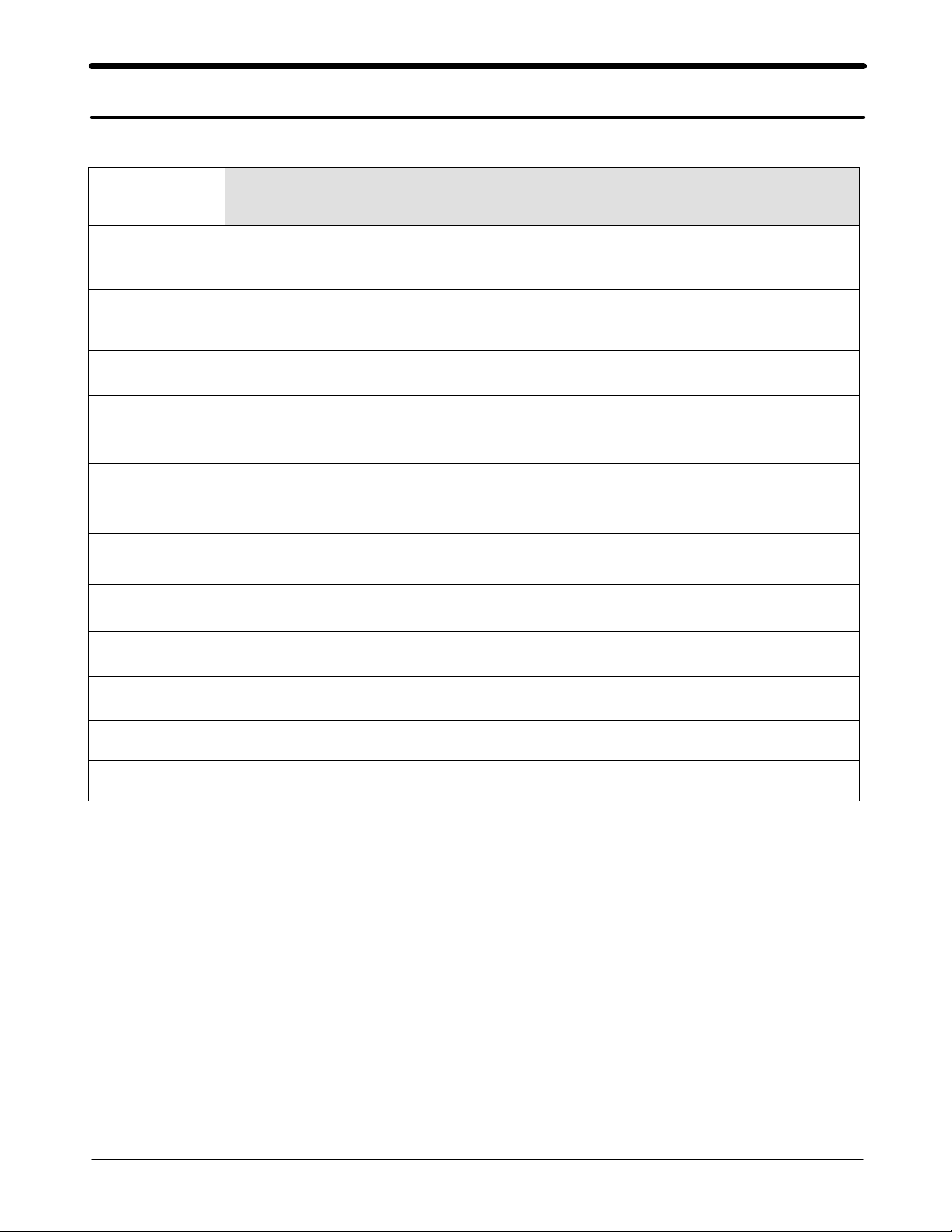
1. Specification
1-1. GSM General Specification
EGSM 900 DCS1800 PCS1900 W-CDMA
Freq.
Band[MHz]
Uplink/Downlink
ARFCN range
Tx/Rx spacing 45MHz 95MHz 80MHz 190MHz
Mod. Bit rate/
Bit Period
Time Slot
Period/Frame
Period
Modulation 0.3GMSK 0.3GMSK 0.3GMSK
MS Power 33dBm~5dBm 30dBm~0dBm 30dBm~0dBm 24dBm ~ - 50dBm
Power Class
880~915
925~960
0~124 &
975~1023
270.833kbps
3.692us
576.9us
4.615ms
4
(max +33dBm)1(max +30dBm)1(max +30dBm)
1710~1785
1805~1880
512~885 512~810
270.833kbps
3.692us
576.9us
4.615ms
1850~1910
1930~1990
270.833kbps
3.692us
576.9us
4.615ms
1920~1980
2110~2170
UL:9612~9888
DL:10562~10838
3.84Mcps
Frame length : 10ms
Slot length : 0.667ms
QPSK
HQPSK
3
(max +24dBm)
Sensitivity -102dBm -100dBm -100dBm -106.7dBm
TDMA Mux 8 8 8
Cell Radius 35Km 2Km 2Km 2Km
1-1
SAMSUNG Proprietary-Contents may change without notice
This Document can not be used without Samsung's authorization
Specification
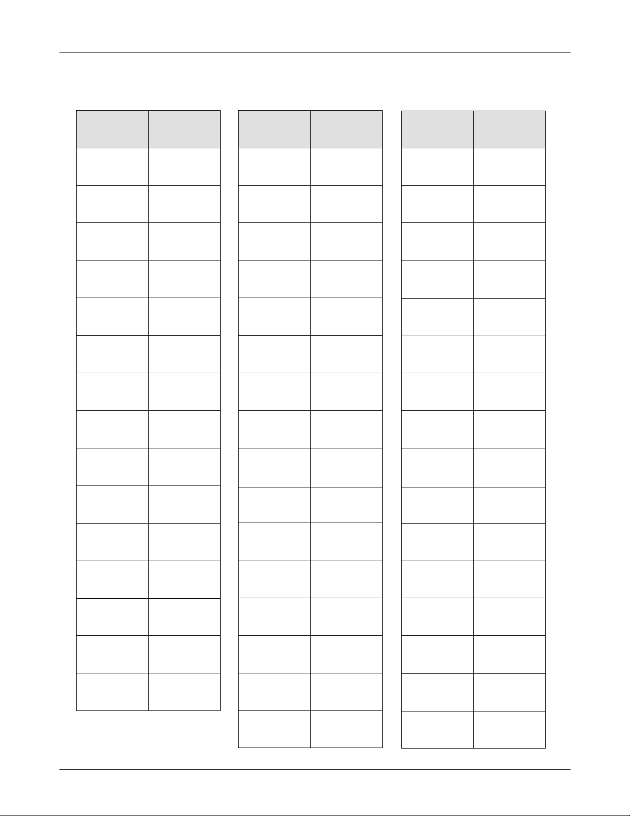
1-2. GSM TX power class
TX Power
control level
5 33±2 dBm
6 31±2 dBm
7 29±2 dBm
8 27±2 dBm
9 25±2 dBm
10 23±2 dBm
11 21±2 dBm
GSM900
TX Power
control level
0 30±3 dBm
1 28±3 dBm
2 26±3 dBm
3 24±3 dBm
4 22±3 dBm
5 20±3 dBm
6 18±3 dBm
DCS1800
TX Power
control level
0 30±3 dBm
1 28±3 dBm
2 26±3 dBm
3 24±3 dBm
4 22±3 dBm
5 20±3 dBm
6 18±3 dBm
PCS1900
12 19±2 dBm
13 17±2 dBm
14 15±2 dBm
15 13±2 dBm
16 11±3 dBm
17 9±3dBm
18 7±3 dBm
19 5±3 dBm
7 16±3 dBm
8 14±3 dBm
9 12±4 dBm
10 10±4 dBm
11 8±4dBm
12 6±4 dBm
13 4±4 dBm
14 2±5 dBm
7 16±3 dBm
8 14±3 dBm
9 12±4 dBm
10 10±4 dBm
11 8±4dBm
12 6±4 dBm
13 4±4 dBm
14 2±5 dBm
15 0±5 dBm
1-2
15 0±5 dBm
SAMSUNG Proprietary-Contents may change without notice
This Document can not be used without Samsung's authorization

2. Circuit Description
2-1. SGH-ZM60 RF Circuit Description
- Antenna Switch Module (U600)
The antenna switch module allows multiple operating bands and modes to share the same antenna. A common
antenna connects to one of five paths: 1) UMTS-2100 Rx/Tx, 2) EGSM-900 Rx, 3) EGSM-900 Tx, 4) DCS-1800
Rx, and 5) DCS-1800 Tx. 6) PCS-1900 Tx, 7) PCS-1900 Rx, UMTS operation requires simultaneous reception
and transmission.
-Filter
To convert Electromagnetic Field Wave to Acoustic Wave and then pass the specific frequency band.
- GSM Rx FILTER (F601)→For filtering the frequency band between 925 ~ 960 MHz.
- DCS Rx FILTER (F602)→For filtering the frequency band 1805 and 1880 MHz.
- DCS Rx FILTER (F603)→For filtering the frequency band 1930 and 1990 MHz.
- WCDMA Rx FILTER (F701)→For filtering the frequency band 2110 and 2170 MHz.
- WCDMA Tx FILTER (F703)→For filtering the frequency band 1920 and 1980 MHz.
- VCTCXO (OSC701)
To generate the 19.2MHz reference clock to drive the logic and RF.
- Duplexer (F202)
A duplexer splits a single operating band into receive and transmit paths.
- UMTS PAM (U701)
This is a key component in the transmitter chain and must complement the RTR6250 IC precisely; jointly they
dominate the UMTS transmitter performance characteristics. Parameters such as gain, output power level, ACLR,
harmonics, Rx-band noise, and power supply current are critical.
- GSM/DCS/PCS PAM (U603)
The PAM is a key component in any transmitter chain and must complement the rest of the transmitter precisely.
For GSM,DCS,PCS operation, the closed-loop transmit power control functions add even more requirements
relative to the UMTS PA. In addition to gain control and switching requirements, the usual RF parameters such
as gain, output power level, several output spectrum requirements, and power supply current are critical.
- GSM/DCS/PCS l Tx VCO (U601)
The Tx VCO outputs for EGSM, DCS, PCS drive a resistive network that splits the active signal into two signals:
1) the input to the active PAM – this is the low loss path, and 2) the OPLL feedback signal.
- RF VCO (OSC702)
The single-band UHF VCO is a key component within its phase-locked loop; VCO performance directly impacts
PLL and transceiver performance. UMTS Rx LO signal is generated from this VCO's output.
2-1
SAMSUNG Proprietary-Contents may change without notice
This Document can not be used without Samsung's authorization

Circuit Description
- RFL6200 (U702)
The RFL6200 includes an LNA circuit optimized for UMTS-2100 operation. The LNA is separated from all other
receive functions contained within the RFR6200 receiver IC to improve mixer LO to RF isolation – a critical
parameter in the Zero-IF architecture.
- RFR6200 (U703)
The RFR6200 provides the Zero-IF receiver signal path, from RF to analog baseband, for UMTS-2100
applications. The RFR6200 accepts its UMTS input signal from the handset RF front-end design. The UMTS input
is configured differentially to optimize second-order inter-modulation and common mode rejection performance, and
implements MSM-controlled gain adjustments to extend the receiver dynamic range.
- RTR6250 (U602)
The RTR6250 supports multi-band, multi-mode phones with two receiver signal paths and three transmitter signal
paths:
Receiver paths
- EGSM-900
-DCS-1800
- PCS-1900
Transmitter paths
- EGSM-900 (using OPLL technique)
- DCS-1800 (using OPLL technique)
- PCS-1900
- UMTS-2100
Numerous secondary functions are integrated on-chip as well:
2-2
SAMSUNG Proprietary-Contents may change without notice
This Document can not be used without Samsung's authorization

Circuit Description
2-2. Baseband Circuit description of SGH-ZM60
2-2-1. PM6650
- Power Management
Ten low-dropout regulators designed specifically for GSM applications power the terminal and help ensure optimal
system performance and long battery life. It provides LDOs support for 1.375V, 1.8V, 2.6V, 2.85V,
3.3V.
IC-level interfaces include the three-line serial bus interface(SBI) used by the MSM6250 device to control
and status the PM6650 IC.
- Keypad Backlight
The Keypad backlight driver output is at pin 23 (KYPD_BACKLIGHT_DRV) and is designed to drive parallel
connected LEDs directly. Its output current level is SBI-programmable and meets the performance specified below.
Input parameters are not specified since they are internal.
- TCXO Controller and Buffers
The PM6650 IC includes circuits for controlling the TCXO warm-up and buffering its signal for distribution
throughout the handset. Performance specifications are presented below.
2-2-2. Connector
- LCD Connector
LCD is consisted of main LCD(color 262K TFT LCD) and small LCD(OLED color 65K LCD). Chip select signals
in the U300, MAIN_LCD_CS can enable main LCD and SUB_LCD_CS can enable small LCD. CAM_PWR_ON
signal enables white LED of main LCD. MAIN_LCD_RESET signal initiates the reset
process of the main LCD. SUB_LCD_RESET signal initiates the Reset process of the small LCD.
16-bit data lines(D2(0)~D(15)) transfers data and commands to LCD. Data and commands use "RS" signal.
If this signal is high, Inputs to LCD are commands. If it is low, Inputs to LCD are data. The signal which informs
the input or output state to LCD, is required. But this system is not necessary this signal.
Power signals for LCD are "VBATT_LCD". "SPKP_RCVP" and "SPKP_RCVN" from HEA401 are used for audio
speaker. And "MOTOR_EN" from U100 enables the motor.
-Key
This is consisted of key interface pins among U100, KEYSENSE_N(0:4). These signals compose the matrix.
Result of matrix informs the key status to key interface in the U100. Power on/off key is seperated from the
matrix. The key LED use the "VBATT" supply voltage. "KEY_LED" signal enables LEDs with current control.
"HALL_SW" informs the status of folder (open or closed) to the. This uses the hall effect IC, A3212ELH.
2-3
SAMSUNG Proprietary-Contents may change without notice
This Document can not be used without Samsung's authorization

Circuit Description
- EMI ESD Filter
This system uses the EMI ESD filter, GMF05LC to protect noise from IF CONNECTOR part.
- IF connetor
It is 24-pin connector. They are designed to use VBATT, CF, UART1_TX, UART1_RX, UART1_RFR,
UART1_CTS, JIG_ON, RTCK, TCK, TDI, TDO, TMS and GND. They connected to power supply IC,
microprocessor and signal processor IC.
2-2-3. Audio
EAR1OP and EAR1ON from U100 are connected to the main speaker. AUXOP and AUXON are connected to
the Digital AMP. MIC1P and MIC1N are connected to the main MIC. And MIC2P and MIC2N are connected to
the Earphone.
YMU769 has a built-in amplifier, and thus, is an ideal device for outputting sounds that are used by mobile
phones in addition to game sounds and ringing melodies that are replayed by a synthesizer.
The synthesizer section adopts "stereophonic hybrid synthesizer system" that are given advantages of both FM
synthesizers and Wave Table synthesizers to allow simultaneous generation of up to 32 FM voices and 32 Wave
Table voices. Furthermore, YMU769 has a built-in hardware sequencer that helps to realize complex play without
heavily loading the host CPU. And this device also has a built-in circuit for controlling vibrators and LEDs
synchronizing with play of music. The consumed electric current can be stopped to the minimum by power down
mode when not operating.
The hardware sequence built in this device allows playing of the complex music without giving excessive load to
the CPU of the portable telephones. Moreover, the registers of the FM synthesizer can be operated directly for
real time sound generation, allowing, for example, utilization of various sound effects when using the game
software installed in the portable telephone.
2-2-4. Memory
The signals in the MSM6250 enable two memories. They use only one volt supply voltage, VDD_LP from
the PM6650. This system uses SEC's memory, KBE00F005M-F411. It is consisted of 1G bits flash NAND
memory and 512M bits SDRAM memory. It has 16 bit data line, D1[0~15] which is connected to MSM6250.
It has 22 bit address lines, A[1~22]. ROM_CS and RAM_CS signals is chip select.
2-2-5. Camera
The camera module consists of Mega pixel and VGA pixel. The Mega camera is a highly integrated CMOS color
image sensor implemented by Hynix COMS sensor process realizing high sensitivity and wide dynamic range.
Total pixel array size is 1184H x 914V, and 1170H x 880V pixels are active. The VGA camera is a
highly integrated CMOS color image sensor implemented by Hynix COMS sensor process realizing high sensitivity
and wide dynamic range. Total pixel array size is 656H x 492V, and 656H x 488V pixels are active.
2-2-6. Irda
This system uses IRDA module, HSDL_3208, Agilent's. This has signals, "IRA_DOWN"(enagle signal),
"RXD0"(Input data) and "TXD0"(output data). These signals are connected to U100(MSN6250). It uses two power
signals. "VDD_LP" is used for circuit and "VBATT" is used for LED.
2-4
SAMSUNG Proprietary-Contents may change without notice
This Document can not be used without Samsung's authorization
 Loading...