

Samsung SGH-X700 Schematics TSHOO
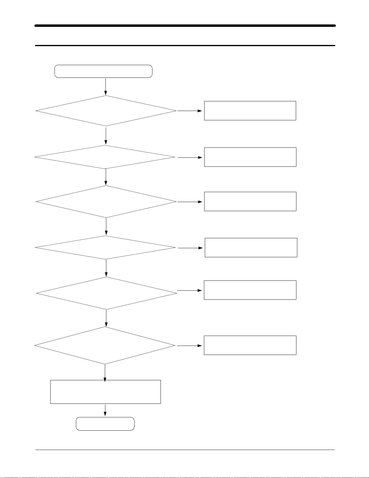
7. Flow Chart of Troubleshooting
7-1. Power On
' Power On ' does not work
Yes
Check the Battery Voltage
is more than 3.4V
Yes
C408(VINT) = 2.7V?
Yes
Check the Clock at
R401=32KHZ
Yes
C427(+VDD_IO_LOW) &
C426(+VDD_IO_HIGH) = "H"?
Yes
No
Charge the Battery
No
Check the PMU related to VINT
No
Resolder OSC400
No
Check the related circuit
C404(+VDD_GSM_CORE)
= 1.875V?
Yes
Check for the clock at C124
= 26MHz
Yes
Check the initial operation
Yes
END
SAMSUNG Proprietary-Contents may change without notice
This Document can not be used without Samsung's authorization
No
No
7-1
Check the +VDD_GSM_CORE circuit
Check the clock generation circuit
(related to TCX100)
Flow Chart of Troubleshooting
ONKEYN
+VDD_RX_TX_2V8
+VCC_SYN_2V8
+VDD_BT_1V8
+VDD_CAM_2V8
+VDD_IO_HIGH_2V9
+VDD_IO_LOW_1V8
C409
C411
VBAT
V400
C413
L402
C415
C416
C417
C424
C426
C427
OSC400
R401
C412
C407
C408
R404
2341
26
27
29
25
28
I
Y
T
C
O
C
E
F
N
C
I
S
E
K
S
V
O
R
N
O
O
_
24
RF2VDD
23
RF12VBAT
22
RF1VDD
21
D1VDD
20
LPD1VBAT
19
LPVDD
18
HCVBAT
17
HCVDD
16
D2VDD
15
IOD2VBAT
14
IOVDD
13
_REC2
S
C
A
I
H
T
B
Q
S
C
R
I
I
R
_
_
M
11
12
10
C425
BAT400
RB414II06N
LCD_BL_ON
C414
R402
R403
BACKLIGHT
T400
32
30
33
36
35
31
34
X
T
V
T
E
D
G
A
V
A
S
V
C
H
O
I
M
I
S
9
A
R
A
D
H
D
B
C
V
G
V
H
C
U400
C
C
1
2
H
H
S
N
N
K
R
E
E
C
R
R
M
I
M
W
W
I
S
_
S
P
P
7
8
6
37
M
B
V
SCP
T
V
P
A
P
C
B
C
/
38
SCN
R
U
C
39
G
D3VDD
H
C
40
SIMD3VBAT
41
SIMVCC
42
SIMIOCD
43
SIMCKCD
44
_SIMRSCD
45
SIMEN
46
GPO3
47
GPO2
48
GPO1
49
GND
50
GND
51
GND
52
K
GND
1
2
3
53
C
NC
L
A
K
E
54
L
C
D
R
NC
_
S
S
C
3
2
1
5
4
C418
+VDD_SD_2V9
+VDD_IO_LOW_1V8
C419
C420
SIM_VCC
SIM_IO
SIM400
SIM_CLK
SIM_RST
C421
6
1
6
1
5
22
5
4
33 4
G
G
G78G
910
C423
AUX_ON
SCL
SDA
32KHz_DIGIT
PON_TX
REF_ON
SIMRST
SIMCLK
MIC_BIAS_2V1
RSTON
IT_PMU
SIMIO
7-2
SAMSUNG Proprietary-Contents may change without notice
This Document can not be used without Samsung's authorization
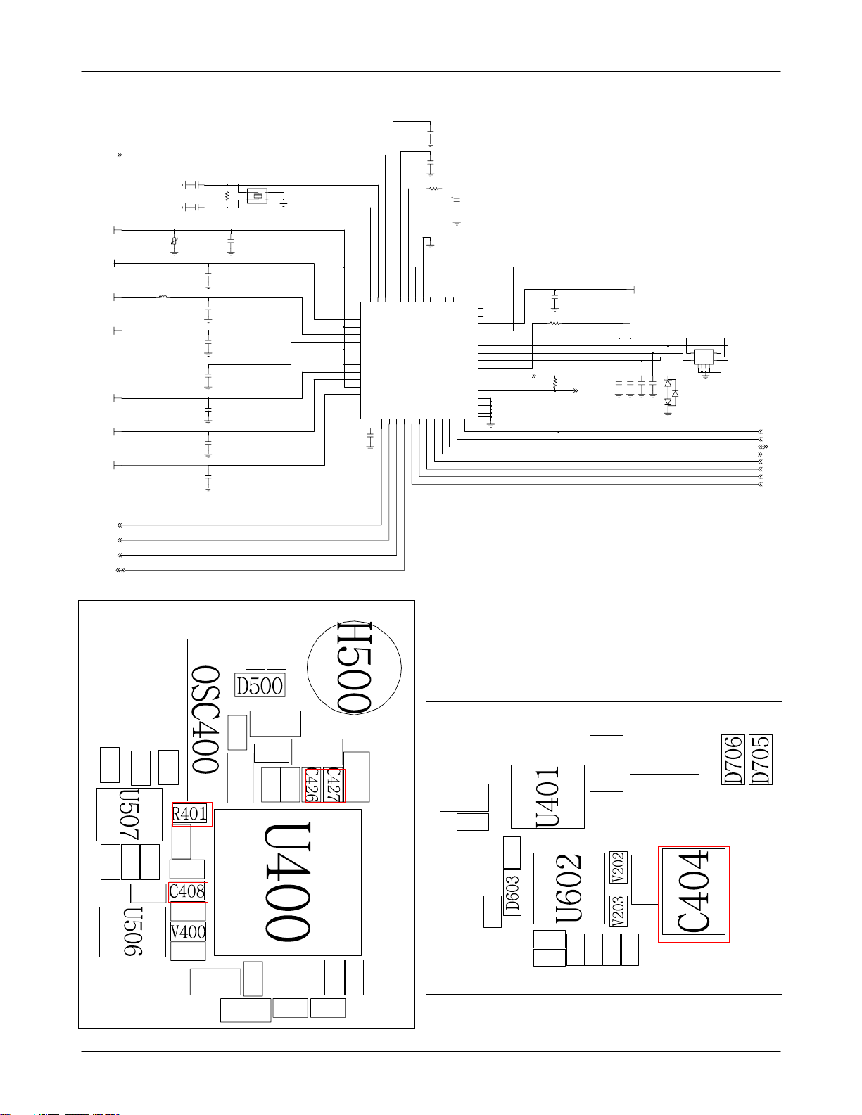
7-2. Initial
Flow Chart of Troubleshooting
Initial Failure
Yes
TP231 (RSTON) ="H"?
Yes
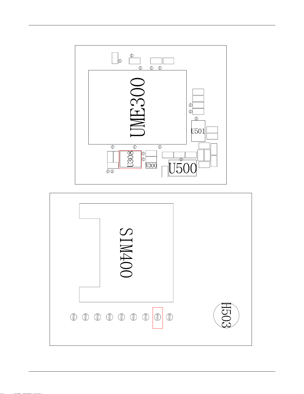
Is U308 pin 4
OK?
Yes
Check the 16bit data signal
&memoryCE
Yes
END
No
Check the circuit related to reset
No
Check the U308
7-3
SAMSUNG Proprietary-Contents may change without notice
This Document can not be used without Samsung's authorization
Flow Chart of Troubleshooting
HA(25)
+VDD_IO_LOW_1V8
GND
OUT
3
IN
2
VCC
NC
1
U308
R300
+VDD_IO_LOW_1V8
+VDD_IO_LOW_1V8
4
5
R317
C304C303 C336
HA(1:16)
HA(1:24)
OEn
CS0n_FLASH
OEn
WEn
CS4n_NAND
BE1n
HA(0)
WEn
CLKBURST
RSTEXTn
CS1n_RAM
ADVn
RSTEXTn
HA(1)
HA(2)
HA(3)
HA(4)
HA(5)
HA(6)
HA(7)
HA(8)
HA(9)
HA(10)
HA(11)
HA(12)
HA(13)
HA(14)
HA(15)
HA(16)
HA(1)
HA(2)
HA(3)
HA(4)
HA(5)
HA(6)
HA(7)
HA(8)
HA(9)
HA(10)
HA(11)
HA(12)
HA(13)
HA(14)
HA(15)
HA(16)
HA(17)
HA(18)
HA(19)
HA(20)
HA(21)
HA(22)
HA(23)
HA(24)
R314
TP315
100K
TP308
B11
N11
N10
P11
N12
G12
F10
E11
G10
F11
K11
K10
L11
L10
D10
E10
D11
C10
C11
D12
H11
G11
H10
P12
J11
J10
B3
B7
P7
N3
P5
P6
B5
N1
N5
N6
N9
F3
L2
F9
G8
G9
H9
K9
K8
K6
C2
D2
E2
C3
D3
E3
C4
F8
C9
D9
E9
G7
B4
D4
E8
D8
D6
P3
N4
M4
L4
E4
C1
C6
C7
B8
B9
E5
D7
G6
E7
C5
J9
N8
P1
P2
P9
1
2
VCCU
VCCU
VCCU
VCCU
VCCU
VCCU
VCCQU
VCCQU
VCCQU
VCCQU
VCCR
VCCR
VCCR
VCCQR
VCCQR
VCCQR
VCCO
VCCO
VCCO
A0O
A1O
A2O
A3O
A4O
A5O
A6O
A7O
A8O
A9O
A10O
A11O
A12O
A13O
A14O
A15O
A0RU
A1RU
A2RU
A3RU
A4RU
A5RU
A6RU
A7RU
A8RU
A9RU
A10RU
A11RU
A12RU
A13RU
A14RU
A15RU
A16RU
A17RU
A18RU
A19RU
A20RU
A21RU
A22RU
A23R
/OEU
/OER
/CER
/OEO
/WEO
/CEO
/WPR
/UBU
/LBU
/WER
/WEU
CLKO
/RESETR
_CSU
INTO
AVDO
_MRSU
VPPR
_RESETO
NC
NC
NC
NC
NC
NC
NC
UME300
VSS
VSS
VSS
VSS
VSS
VSS
VSS
VSS
VSS
VSS
VSS
VSS
DQ0O
DQ1O
DQ2O
DQ3O
DQ4O
DQ5O
DQ6O
DQ7O
DQ8O
DQ9O
DQ10O
DQ11O
DQ12O
DQ13O
DQ14O
DQ15O
DQ0RU
DQ1RU
DQ2RU
DQ3RU
DQ4RU
DQ5RU
DQ6RU
DQ7RU
DQ8RU
DQ9RU
DQ10RU
DQ11RU
DQ12RU
DQ13RU
DQ14RU
DQ15RU
DNU
DNU
DNU
DNU
DNU
DNU
DNU
DNU
DNU
DNU
DNU
CLKRU
RDYR_WAITU
RDYO
_AVDRU
B2
B10
C8
E12
F2
J12
K2
M2
N2
P4
P8
P10
M3
L5
K5
J4
J3
H4
G3
G5
K4
L3
K3
J5
H3
H5
G4
F4
M5
L6
M6
N7
K7
M8
L9
M10
J7
J8
M7
L7
L8
H8
M9
M11
A2
A3
A10
A11
A12
R1
R2
R3
R10
R11
R12
E6
D5
F5
F6
B1
NC
B6
NC
B12
NC
C12
NC
D1
NC
E1
NC
F1
NC
F7
NC
F12
NC
G1
NC
G2
NC
H1
NC
H2
NC
H12
NC
H6
NC
H7
NC
J1
NC
J2
NC
J6
NC
K12
NC
K1
NC
L1
NC
L12
NC
M1
NC
M12
NC
HD(0)
HD(1)
HD(2)
HD(3)
HD(4)
HD(5)
HD(6)
HD(7)
HD(8)
HD(9)
HD(10)
HD(11)
HD(12)
HD(13)
HD(14)
HD(15)
HD(0)
HD(1)
HD(2)
HD(3)
HD(4)
HD(5)
HD(6)
HD(7)
HD(8)
HD(9)
HD(10)
HD(11)
HD(12)
HD(13)
HD(14)
HD(15)
TP316
TP307
R312
MEMORY
HD(0:15)
HD(0:15)
CLKBURST
WAITn
ADVn
+VDD_IO_LOW_1V8
7-4
SAMSUNG Proprietary-Contents may change without notice
This Document can not be used without Samsung's authorization
Flow Chart of Troubleshooting
7-5
SAMSUNG Proprietary-Contents may change without notice
This Document can not be used without Samsung's authorization
Flow Chart of Troubleshooting
7-3. Charging Part
Abnormal charging part
Yes
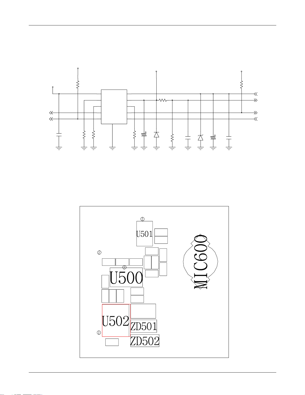
Check the U502 pin 10
>4.9V
Yes
U502 pin 6 = "L"?
Yes
U502 pin 4 = "L"?
Yes
Check the U502 pin 9
≒4.2V
No
No
No
No
Check the circuit related to
V_EXT_CHARGE
Resolder or replace U502
Check the circuit related to
AUX_ON signal
Resolder or replace U502
Yes
END
7-6
SAMSUNG Proprietary-Contents may change without notice
This Document can not be used without Samsung's authorization
Flow Chart of Troubleshooting
+VDD_IO_HIGH_2V9
+VBUS
AUX_ON USB_IN
END_OF_CHG CHG_ON
C506
R518
R520
R521
1
2
4
5
USBIN
IUSB
ITERM
PWR
CHRG
U502
10
DCIN
9
BAT
83
IDC
7
USBPWR
6
EN
GND
11
R522
C507
VBAT
R519
ZD502
R523
ZD501
C502
C504
+VDD_IO_HIGH_2V9
R517
V_EXT_CHARGE
MES_BATT
C503
7-7
SAMSUNG Proprietary-Contents may change without notice
This Document can not be used without Samsung's authorization
Flow Chart of Troubleshooting
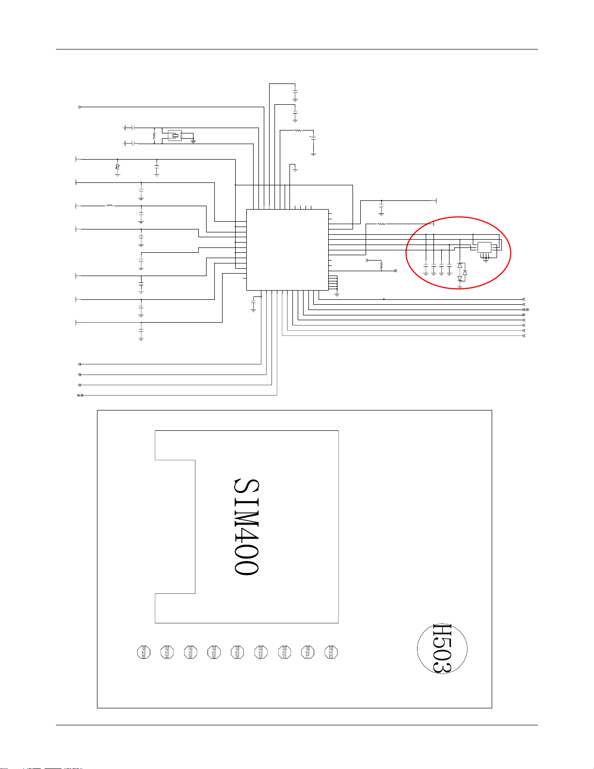
7-4. Sim Part
Phone can't access SIM Card
SIM400 pin 1,5 = "H"?
Yes
No
Check the sim charge pump
Yes
After Power ON,
Check SIMCLK Signal on
pin3 of SIM400 in a few
Yes
After SIM card insert,
SIM400 pin 2 = "H(SIM_RST)"?
Yes
Check the SIM Card
Yes
END
No
Check the Clock
No
Replace PBA
7-8
SAMSUNG Proprietary-Contents may change without notice
This Document can not be used without Samsung's authorization
+VDD_RX_TX_2V8
+VCC_SYN_2V8
+VDD_BT_1V8
+VDD_CAM_2V8
+VDD_IO_HIGH_2V9
+VDD_IO_LOW_1V8
ONKEYN
VBAT
Flow Chart of Troubleshooting
C407
C408
C409
C411
V400
C413
L402
C415
C416
C417
C424
C426
C427
OSC400
R401
C412
2341
27
25
26
I
O
C
C
S
S
O
O
24
RF2VDD
23
RF12VBAT
22
RF1VDD
21
D1VDD
20
LPD1VBAT
19
LPVDD
18
HCVBAT
17
HCVDD
16
D2VDD
15
IOD2VBAT
14
IOVDD
13
_REC2
S
A
I
B
C
I
M
12
C425
R404
BAT400
RB414II06N
LCD_BL_ON
C414
R402
R403
BACKLIGHT
T400
34
32
29
30
28
33
36
35
31
X
T
Y
E
K
N
O
_
C
H
T
S
R
_
V
T
E
T
C
F
N
I
E
V
R
Q
R
I
_
11
10
D
G
A
A
A
V
R
D
H
A
D
B
C
S
V
G
V
V
H
C
U400
C
C
H
1
2
C
H
S
N
N
H
K
R
E
E
O
I
C
R
R
M
I
M
M
I
I
W
W
S
_
S
S
P
P
8
7
6
9
37
M
B
V
SCP
T
V
P
A
P
C
C
B
38
/
SCN
R
U
C
39
G
D3VDD
H
C
40
SIMD3VBAT
41
SIMVCC
42
SIMIOCD
43
SIMCKCD
44
_SIMRSCD
45
SIMEN
46
GPO3
47
GPO2
48
GPO1
49
GND
50
GND
51
GND
52
K
GND
1
2
3
53
C
NC
A
L
K
E
54
L
D
C
R
NC
_
S
S
C
3
2
1
5
4
C418
+VDD_SD_2V9
+VDD_IO_LOW_1V8
C420
C419
SIM_VCC
SIM_IO
SIM400
SIM_CLK
SIM_RST
C421
6
1
6
1
5
22
5
4
33 4
G
G
G78G
910
C423
AUX_ON
SCL
SDA
32KHz_DIGIT
PON_TX
REF_ON
SIMRST
SIMCLK
MIC_BIAS_2V1
RSTON
IT_PMU
SIMIO
7-9
SAMSUNG Proprietary-Contents may change without notice
This Document can not be used without Samsung's authorization
 Loading...