

Samsung SGH-X700 Schematics CDESC
2. Circuit Description
2-1. SGH-X700 RF Circuit Description
2-1-1. RX PART
- FRONT END MODULE(ANTENNA SWITCH MODULE + RX SAW FILTER) (U100)
It performs to switch Tx & Rx paths for GSM900, DCS1800 and PCS1900 with logic controls below.
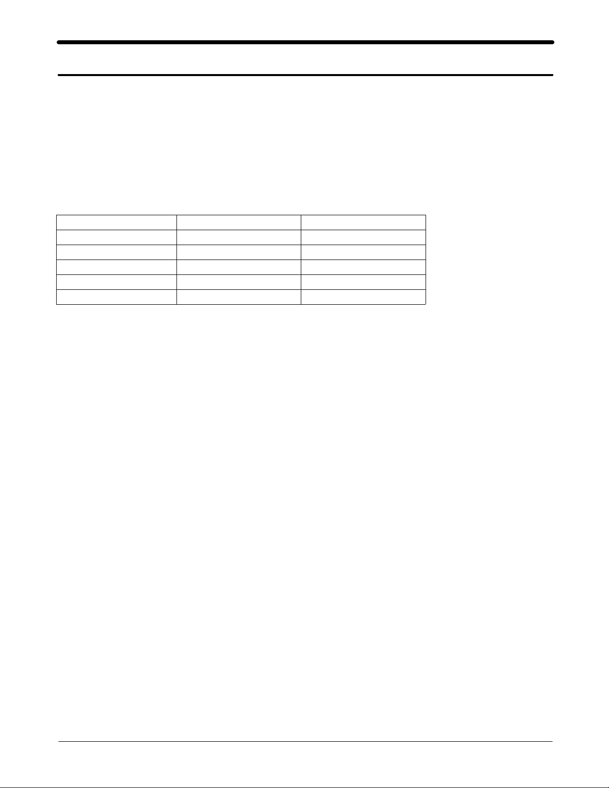
- FEM Control Logic Table
FESW1 FESW2
Tx Mode (GSM900) H L
Tx Mode (DCS1800/1900) L H
Rx Mode (GSM900) L L
Rx Mode (DCS1800) L L
Rx Mode (PCS1900) L L
- VC-TCXO (TCX100)
This module generates the 26MHz reference clock to drive the logic and RF systems.
It is turned on when the supply voltage (+VCC_SYN_2V8) is applied.
After buffering, the 26MHz reference clock is supplied to the other parts of the system through the transceiver pin
CLKOUT.
- Transceiver (U102)
This chip is fully integrated GSM & GPRS tri-band transceiver with RF VCO, loop filters and most of the
passive components required in it.
It also fully integrated fractional N RF synthesizer with AFC control possibility, RF VCO with integrated supply
regulator. Semi integrated reference oscillator with integrated supply regulator.
RF Receiver front-end amplifies the E-GSM900, DCS1800 and PCS1900 aerial signal, convert the chosen channel
down to a low IF of 100kHz.
In IF section, further amplifies the wanted channel, performs gain control to tune the output level to the desired value and
rejects DC.
2-1-2. TX PART
The transmitter is fully differential using a direct up conversion architecture. It consists of a signal side band
power up mixer. Gain is controlled by 6 dB via 3-wire serial bus programing. The fully integrated VCO and power
mixer achieve LO suppression, quadrature phase error, quadrature amplitude balance and low noise floor specification.
Output matching/balun components drive a standard 50 ohms single ended load.
2-1
SAMSUNG Proprietary-Contents may change without notice
This Document can not be used without Samsung's authorization

Circuit Description
2-2. Baseband Circuit description of SGH-X700
2-2-1. PCF50603 (U400)
- Power Management
Eight low-dropout regulators designed specifically for GSM applications power the terminal and help ensure optimal
system performance and long battery life. A programmable boost converter provides support for 1.8V, 3.0V SIMs,
while a self-resetting, electronically fused switch supplies power to external accessories. Ancillary support functions,
such as RTC module and High Voltage Charge pump, Clock generator, aid in reducing both board area and system
complexity.
I2C BUS serial interface provides access to control and configuration registers. This interface gives a microprocessor
full control of the PCF50603 and enables system designers to maximize both standby and talk times.
Supervisory functions. including a reset generator, an input voltage monitor, and a temperature sensor, support reliable
system design. These functions work together to ensure proper system behavior during start-up or in the event of a
fault condition(low microprocessor voltage, insufficient battery energy, or excessive die temperature).
- Pulse-Width Modulator
The Backlight Brightness Modulator (BBM) contains a programmable Pulse-width modulator (PWM) to modulate the
intensity of a series of LED's or to control a DC/DC converter that drives LCD backlight.
This phone is using PWM control to modulate the LCD backlight brightness.
- Clock Generator
The Clock Generator (CG) generates all clocks for internal and external usage. The 32.768 kHz crystal oscillator
provides an accurate low clock frequency for the PCF50603 and other circuitry.
2-2-2. LCD
X700 has just one 1.9" TFT LCD. 16-bit data lines(LD(0)~LD(15)) transfers data and commands to LCD. There are
couple of control signals such as RS, CS, RD, WR, etc. RS stands for "Register Select pin." When RS = 0, data can be
written to the index register or status can be read, and when RS = 1, an instruction can be issued or data can be written
to or read from RAM. Read or write operation is selected according to RD/WR signals. The data is received when the
R/W bit is 0, and is transmitted when the R/W bit is 1.
At the falling edge of CS input, serial data transfer is
initiated. On the other hand, at the rising edge of CS input, the data transfer is ceased.
2-2-3. Key
Key recognition part is consisted of 8 ports from PCF5213EL1. KEY_ROW(0:4) & KEY_COL(0:4)
These signals performs with the matrix. Any input from the matrix informs the key status to key interface in the
PCF5213EL1. Power on/off key is independent of the matrix. Therefore, 'power on/off' signal is directly connected with
PCF50603 to turn PCF50603 on.
3.3V LDO(U700) enables Key LED on. Key LED consists of 12 LEDs. It is controlled by "Key_led_on" signal.
2-2
SAMSUNG Proprietary-Contents may change without notice
This Document can not be used without Samsung's authorization
 Loading...