

Samsung SGH-X640 Service Manual

SAMSUNG Anycall
SGH-X640
SAMSUNG Anycall
CONTENTS
1. Specification
2. Circuit Description
3. Exploded Views and Parts List
4. Electrical Parts List
5. Block Diagrams
6. PCB Diagrams
7. Flow Chart of Troubleshooting
This Service Manual is a property of Samsung Electronics Co.,Ltd.
Any unauthorized use of Manual can be punished under applicable
International and/or domestic law.
ⓒ
Samsung Electronics Co.,Ltd. March. 2005
PrintedinKorea.
Code No.: GH68-06819A
BASIC.
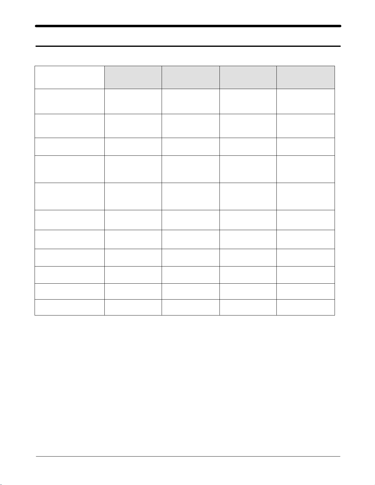
1. Specification
1. GSM General Specification
GSM900
Phase 1
Freq. Band[MHz]
Uplink/Downlink
ARFCN range 1~124
Tx/Rx spacing 45MHz 45MHz 95MHz 80MHz
Mod. Bit rate/
Bit Period
Time Slot
Period/Frame Period
Modulation 0.3GMSK 0.3GMSK 0 .3GMSK 0.3GMSK
MS Power 33dBm~13dBm 33dBm~5dBm 30dBm~0dBm 30dBm~0dBm
890~915
935~960
270.833kbps
3.692us
576.9us
4.615ms
EGSM 900
Phase 2
880~915
925~960
0~124 &
975~1023
270.833kbps
3.692us
576.9us
4.615ms
DCS1800
Phase 1
1710~1785
1805~1880
512~885 512~810
270.833kbps
3.692us
576.9us
4.615ms
1850~1910
1930~1990
270.833kbps
PC1900
Phase 1
3.692us
576.9us
4.615ms
Power Class 5pcl ~ 15pcl 5pcl ~ 19pcl 0pcl ~ 15pcl 0pcl ~ 15pcl
Sensitivity -102dBm -102dBm -100dBm -100dBm
TDMA Mux 8 8 8 8
Cell Radius 35Km 35Km 2Km 2Km
1-1
SAMSUNG Proprietary-Contents may change without notice
This Document can not be used without Samsung's authorization
Specification
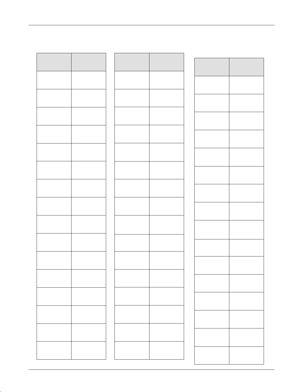
2. GSM TX power class
TX Power
control level
5 33±2 dBm
6 31±2 dBm
7 29±2 dBm
8 27±2 dBm
9 25±2 dBm
10 23±2 dBm
11 21±2 dBm
GSM900
TX Power
control level
0 30±3 dBm
1 28±3 dBm
2 26±3 dBm
3 24±3 dBm
4 22±3 dBm
5 20±3 dBm
6 18±3 dBm
DCS1800
TX Power
control level
0 30±3 dBm
1 28±3 dBm
2 26±3 dBm
3 24±3 dBm
4 22±3 dBm
5 20±3 dBm
6 18±3 dBm
PCS1900
12 19±2 dBm
13 17±2 dBm
14 15±2 dBm
15 13±2 dBm
16 11±3 dBm
17 9±3dBm
18 7±3 dBm
19 5±3 dBm
7 16±3 dBm
7 16±3 dBm
8 14±3 dBm
8 14±3 dBm
9 12±4 dBm
9 12±4 dBm
10 10±4 dBm
10 10±4 dBm
11 8±4dBm
11 8±4dBm
12 6±4 dBm
12 6±4 dBm
13 4±4 dBm
13 4±4 dBm
14 2±5 dBm
14 2±5 dBm
15 0±5 dBm
15 0±5 dBm
1-2
SAMSUNG Proprietary-Contents may change without notice
This Document can not be used without Samsung's authorization
2. Circuit Description
1. SGH-
X640
RF Circuit Description
1) RX PART
1. ASM(U103)→Switching Tx, Rx path for GSM900, DCS1800, PCS1900 by logic controlling.
2. ASM Control Logic (U103)
GSM Tx Mode H L L
DCS Tx Mode L H L
PCS Tx Mode H L L
GSM Rx Mode L L L
DCS Rx Mode L L L
PCS Rx Mode L L H
3. FILTER
To convert Electromagnetic Field Wave to Acoustic Wave and then pass the specific frequency band.
- GSM FILTER (F100)→For filtering the frequency band between 925 and 960 MHz
- DCS FILTER (F102)→For filtering the frequency band between 1805 and 1880 MHz.
- PCS FILTER (F101)→For filtering the frequency band between 1930 and 1990 MHz.
→
Truth Table
VC1 VC2 VC3
4. VC-TCXO (OSC100)
This module generates the 26MHz reference clock to drive the logic and RF. After division by two a reference clock of
13MHz is supplied to the other parts of the system through the pin CLKOUT. After additional process, the reference
clock applies to the U100 Rx IQ demodulator and Tx IQ modulator. And then, the oscillator is controlled by serial data
to select channel and use fast lock mode for GPRS high class operation.
5. Transceiver (U100)
The receiver front-end which amplifies the GSM, DCS aerial signal, converts the chosen channel down to a low IF signal
of 100 kHz. The first stages are symmetrical low noise amplifiers (LNAs). The LNAs are followed by an IQ down mixer.
It consists of two mixers in parallel but driven by quadrature out of phase LO signals. The In phase (I) and Quadrature
phase (Q) IF signals are low pass filtered to provide protection from high frequency offset interferes. The low IF I and Q
signals are then fed into the channel filter. The front-end low IF I and Q outputs enter the integrated bandpass channel
filter with provision for five 8 dB gain steps in front of the filter.
2) TX PART
I and Q baseband signals are applied to the IQ modulator that shifts the modulation spectrum up to the transmit IF. It is
designed for low harmonic distortion, low carrier leakage and high image rejection to keep the phase error as small as
possible.
2-1
SAMSUNG Proprietary-Contents may change without notice
This Document can not be used without Samsung's authorization
Circuit Description
The modulator is loaded at its IF output by an integrated low pass filter that suppress unwanted spurs prior to get into
the phase detector. The clock drive is generated by division of the RFLO signal provided for the transmit offset mixer.
Baseband IQ signal fed into offset PLL, this function is included inside of U100 chip. OSC101 chip generates modulator
signal which power level is about 6.5dBm and fed into Power Amplifier(U102). The PA output power and power ramping
are well controlled by Auto Power Control circuit. We use offset PLL below table.
GSM -35dBc
DCS -35dBc
GSM -66dBc
DCS -65dBc
GSM -75dBc
DCS -68dBc
Modulation Spectrum
200kHz offset
30 kHz bandwidth
400kHz offset
30 kHz bandwidth
600kHz ~ 1.8MHz offset
30 kHz bandwidth
2. Baseband Circuit description of SGH-X640
1. PCF50601
1.1. Power Management
Ten low-dropout regulators designed specifically for GSM applications power the terminal and help ensure optimal system
performance and long battery life. A programmable boost converter provides support for 1.8V, 3.0V, and 5.0V SIMs,
while a self-resetting, electronically fused switch supplies power to external accessories. Ancillary support functions, such
as RTC module and High Voltage Charge pump, Clock generator, aid in reducing both board area and system complexity.
I2C BUS serial interface provides access to control and configuration registers. This interface gives a microprocessor full
control of the PCF50601 and enables system designers to maximize both standby and talk times.
Supervisory functions. including a reset generator, an input voltage monitor, and a temperature sensor, support reliable
system design. These functions work together to ensure proper system behavior during start-up or in the event of a fault
condition(low microprocessor voltage, insufficient battery energy, or excessive die temperature).
Backlight Brightness Modulator
1.2.
The Backlight Brightness Modulator (BBM) contains a programmable Pulse-width
to modulate the intensity of a series of LED’s or to control a DC/DC converter that drives LCD backlight.
But, this phone (SGH-X640) is use UFB LCD. UFB LCD controls backlight brightness by contrast setting.
So "BL_VDD" voltage is always high value when phone is in active mode. When phone is in dimming mode "BL_VDD"
goes to about 10% duty PWM.
Clock Generato
1.3.
The Clock Generator (CG) generates all clocks for internal and external usage. The 32768 Hz crystal
oscillator provides an accurate low clock frequency for the PCF50601 and other circuitry.
r
modulator (PWM) and FET
2. LCD Connector
LCD is consisted of main LCD(color 65K UFB LCD).
Chip select signals LCD_MAIN_CS can enable LCD. BACKLIGHT signal enables white LED of main LCD.
"RESET_2V8" signal initiates the reset process of the LCD.
2-2
SAMSUNG Proprietary-Contents may change without notice
This Document can not be used without Samsung's authorization

Circuit Description
16-bit data lines(LD(0)~LD(15)) transfers data and commands to LCD through bypass capacitor. Data and commands use
"RS" signal. If this signal is high, inputs to LCD are commands. If it is low, inputs to LCD are data.
The signal which informs the state of LCD is whether input or output, is required. But in this system, there is no input
state from LCD. So only "L_WR" signal is used to indicate write data or command to LCD. Power signals for LCD are
"VBAT and "VDD2".
"M_SCL", "M_SCA", "PCLK", "FVALID", "LVALID" and "STANDBY" signals are all related to camera working.
"SVC_LED" is signal for service led when the signal is low led is on and vice versa. "SPK_P" and "SPK_N" are used
for audio speaker containing voice or melody. And "VDD_VIB" from PCF50601 enables the motor.
3. Key
This is consisted of key interface pins among OM6359, KBIO(0:7). These signals compose the matrix. Result of matrix
informs the key status to key interface in the OM6359. Power on/off key is separated from the matrix. So power on/off
signal is connected with PCF50601 to enable PCF50601. Fifteen key LEDs are use the "VBAT" as supply voltage.
"VDD_KEY" signal enables LEDs. "FLIP" informs the status of folder (open or closed) to the OM6359. This uses the
hall effect IC, SH248CSP. A magnet under main LCD enables SH248CSP.
4. EMI ESD Filter
This system uses the EMI ESD filter, EMIF09 to protect noise from IF CONNECTOR part.
5. IF connetor
It is 18-pin connector. They are designed to use VBAT, V_EXT_CHARGE, TXD0, RXD0, RTS0, CTS0, JIG_REC,
CHARGER_OK, RXD1, TXD1, AUX_MIC, AUX_SPK and GND. They connected to power supply IC, microprocessor
and signal processor IC.
6. Battery Charge Management
A complete constant-current/constant-voltage linear charger is used for single cell lithium-ion batteries.
If TA connected to phone, "V_EXT_CHARGE" enable charger IC and supply current to battery.
When fault condition caused, "CHG_ON" signal level change low to high and charger IC stop charging
process.
7. Audio
EARP_P and EARP_N from OM6359 are connected to the main speaker. AUXSP is connected to the Hands free kit.
MIC_P and MIC_N are connected to the main MIC. And AUX_MIC_P and AUX_MIC_N are connected to the Hands
free kit.
YMU762C is a LSI for portable telephone that is capable of playing high quality music by utilizing FM synthesizer and
ADPCM decoder that are included in this device.
As a synthesis, YMU762C is equipped 32 voices with different tones. Since the device is capable of simultaneously
generating up to synchronous with the play of the FM synthesizer, various sampled voices can be used as sound effects.
Since the play data of YMU762C are interpreted at anytime through FIFO, the length of the data(playing period) is not
limited, so the device can flexibly support application such as incoming call melody music distribution service. The
hardware sequencer built in this device allows playing of the complex music without giving excessive load to the CPU of
the portable telephones.
2-3
SAMSUNG Proprietary-Contents may change without notice
This Document can not be used without Samsung's authorization

Circuit Description
Moreover, the registers of the FM synthesizer can be operated directly for real time sound generation, allowing, for
example, utilization of various sound effects when using the game software installed in the portable telephone.
YMU762C includes a speaker amplifier with high ripple removal rate whose maximum output is 550mW (SPVDD=3.6V).
The device is also equipped with conventional function including a vibrator and a circuit for controlling LEDs
synchronous with music.
For the headphone, it is provided with a stereophonic output terminal.
For the purpose of enabling YMU762C to demonstrate its full capabilities, Yamaha purpose to use "SMAF:Synthetic music
Mobile Application Format" as a data distribution format that is compatible with multimedia. Since the SMAF takes a
structure that sets importance on the synchronization between sound and images, various contents can be written into it
including incoming call melody with words that can be used for training karaoke, and commercial channel that combines
texts, images and sounds, and others. The hardware sequencer of YMU762C directly interprets and plays blocks relevant
to synthesis (playing music and reproducing ADPCM with FM synthesizer) that are included in data distributed in SMAF.
8. Memory
Signals in the OM6359 enable two memories. They use only one volt supply voltage, VDD3 in the PCF50601. This
system uses Samsung's memory, KBB06A500M-T402. It is consisted of 128M bits flash NOR memory and 128M bits
flash NAND memory and 64M bits SCRAM. It has 16 bit data line, HD[0~15] which is connected to OM6359 and
MV317S. It has 26 bit address lines, HA[1~26]. CS_NAND and NCSRAM signals are chip select. Writing process,
HWR_N is low and it enables writing process to flash memory and SRAM. During reading process, HRD_N is low and
it enables reading process to flash memory and SRAM. Each chip select signals in the OM6359 select memory among 2
flash memory and SCRAM. Reading or writing procedure is processed after HWR_N or HRD_N is enabled. Memories
use reset, which is VDD3 delay from PCF50601. HA[25] signal enables lower byte of SRAM and HA[26] signal enables
higher byte of SRAM.
9. OM6359
OM6359 is consisted of ARM core and DSP core. It has
on-chip program ROM
of KBS, JTAG, EMI and UART. ARM core is consisted of EMI, PIC(Programmable Interrupt Controller),
reset/power/clock unit, DMA controller, TIC(Test Interface Controller), peripheral bridge, PPI, SSI(Synchronous Serial
Interface), ACC(Asynchronous communications controllers), timer, ADC, RTC(Real-Time Clock) and keyboard interface.
KBIO(0:7), address lines of DSP core and HD[0~15]. HA[1~26], address lines of ARM core and HD[0~15], data lines of
ARM core are connected to memory, YMU762C. MV317S(Camera DSP Chip) controls the communication between ARM
core and DSP core.
CS_NAND, NCSRAM, NCSFLASH in the ARM core are connected to each memory. HWR_N and HRD_N control the
process of memory. External IRQ(Interrupt ReQuest) signals from each units, such as, PMU need the compatible process.
KBIO[0~7] receive the status from key and RXD0/TXD0 are used for the communication using data link
cable(DEBUG_DTR/RTS/TXD/RXD/CTS/DSR).
It has JTAG control pins(TDI/TDO/TCK) for ARM core and DSP core. It receives 13MHz clock in CKI pin from
external TCXO. ADC(Analog to Digital Convertor) part receives the status of temperature, battery type and battery voltage.
in the DSP. It has 4K*32bits ROM and 2K*32bits RAM in the ARM core. DSP is consisted
8x1Kword on-chip program/data RAM, 55 Kwords
2-4
SAMSUNG Proprietary-Contents may change without notice
This Document can not be used without Samsung's authorization

Circuit Description
10. TOH2600DGI4KRA(26MHz)
This system uses the 26MHz TCXO, TOH2600DGI4KRA, SEM. AFC control signal from OM6359 controls frequency
from 26MHz x-tal. The clock output frequency of UAA3536 is 13MHz. This clock is connected to OM6359, YMU762C.
11. Camera DSP(MV317S)
Tiger is an Integrated circuit for mobile phone camera. This structure will allow effectiveness for large
data management and significantly reduces main processor will get burden.
In hence, Tiger will allow the user to be able to display to LCD direct without burdening the main
processor. It also allows to have various kinds of display size on the LCD and snapshot for Jpeg. Digital
effect will also be executed on real time base resulting Tiger as being a video co-processor in the
mobile platform. Also,an
interchange the data with Tiger. As the additional 8Mbit is usable except 2Mbit buffer embedded in Tiger, the diverse UI
data processing which is not a
ISO/IEC 10918-1 JPEG compliance (DCT-based). JPEG decoder supports YUV444, YUV422, YUV420 and
YUV411 format standard JPEG image.
i80 type processor’ s 16bit parallel interface of Tiger makes it available for the CPU to
burden to the CPU is available. JPEG encoder and decoder are baseline
2-5
SAMSUNG Proprietary-Contents may change without notice
This Document can not be used without Samsung's authorization

Circuit Description
2-6
SAMSUNG Proprietary-Contents may change without notice
This Document can not be used without Samsung's authorization
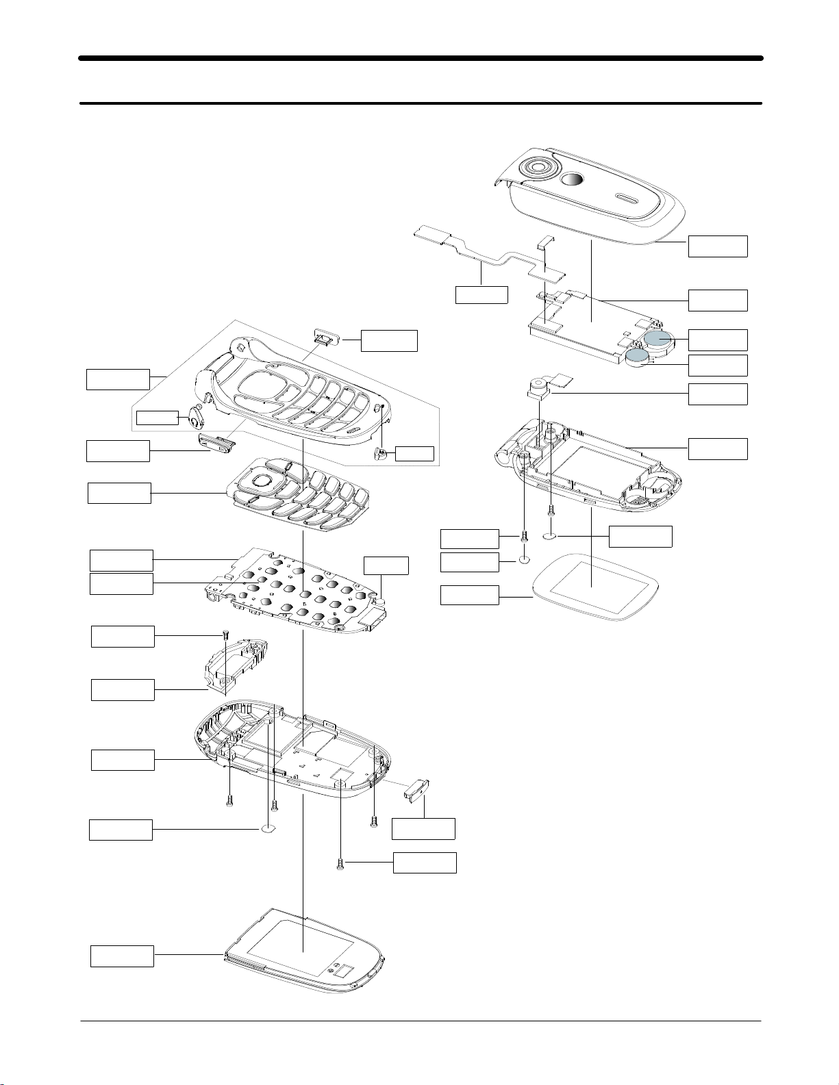
3. Exploded View and Parts list
1. Cellular phone Exploded View
QFU01
QFR01
QVO01
QKP01
QMP01
QME01
QCR08
QAN02
QRF03
QCK01
QMI03
QMI01
QPC01
QCR17
QSC08
QMW02
QLC01
QSP01
QMO01
QCA01
QFL01
QSC05
QRE01
QRF01
QBA01
QIF01
QCR21
3-1
SAMSUNG Proprietary-Contents may change without notice
This Document can not be used without Samsung's authorization
Exploded view and Part list
2. Cellular phone Parts list
Location
Description SEC CODE Remark
NO.
QFU01 FOLDER UPPER GH75-06199A
QLC01 LCD GH07-00653A
QPC01 FPCB GH41-00774A
QSP01 SPEAKER 3001-001731
QMO01 MOTOR DC 3101-001401
QCA01 UNIT CAMERA GH59-01472A
QFL01 FOLDER LOWER GH75-06200A
QSC05 SCREW SHEET R GH74-08872A
QSC08 SCREW SHEET L GH74-08873A
QCR17 SCREW MACHINE 6001-001639
QMW02 WINDOW MAIN GH72-19197A
QFR01 FRONT COVER GH75-06331A
QRF03 EAR COVER GH72-19199A
QMI03 MIC RUBBER GH73-04064A
QCK01 CAMERA KEY GH75-06567A
QVO01 VOLKEY ASSY GH75-06566A
QKP01 KEYPAD GH75-06201A
QMP01 MAIN PBA GH92-02030A
QME01 UNIT METAL DOME GH59-01921A
QMI01 MICROPHONE ASSY GH30-00130A
QCR08 SCREW MACHINE 6001-001456
QAN02 INTENNA GH42-00523A
QRE01 REAR COVER GH75-06202A
QRF01 RF SHEET GH74-13063A
QIF01 IF COVER GH72-19208A
QCR21 SCREW MACHINE 6001-001507
QBA01 BATTERY GH43-01658A
3-2
SAMSUNG Proprietary-Contents may change without notice
This Document can not be used without Samsung's authorization
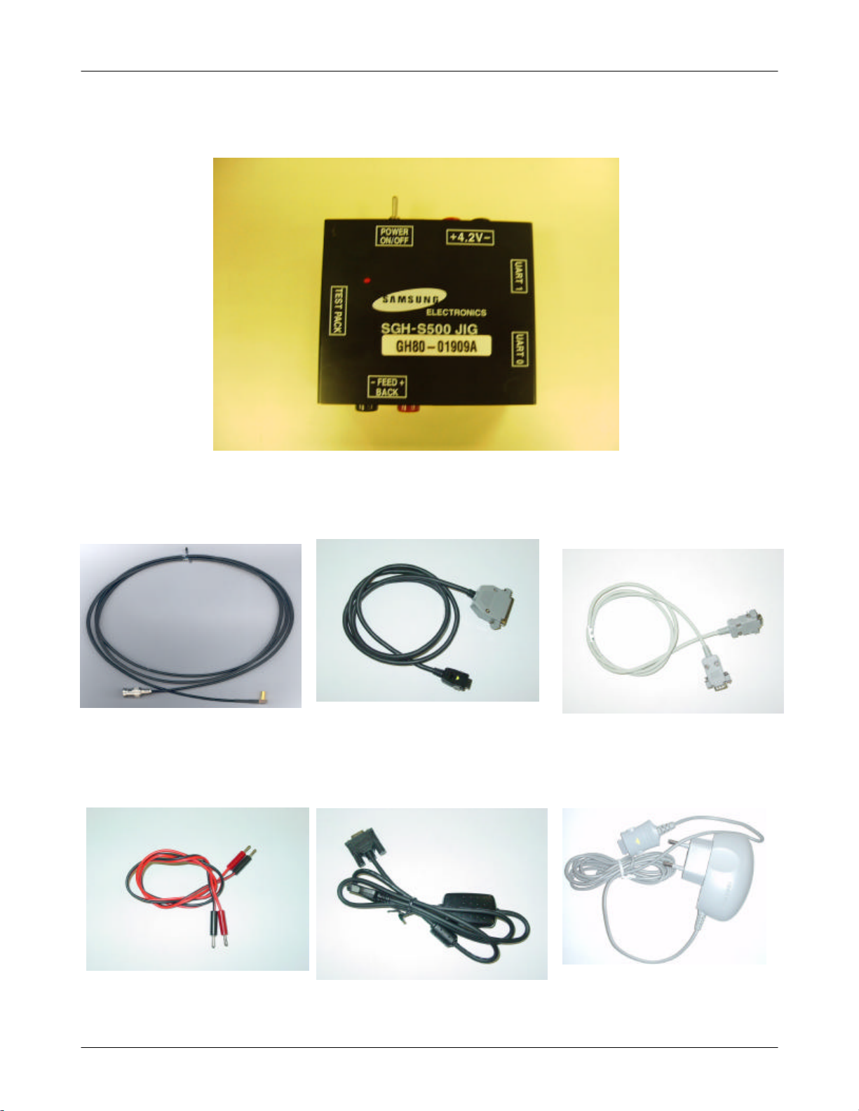
3. Test Jig (GH80-01909A)
Exploded view and Part list
3-1. RF Test Cable
(GH39-00283A)
3-2. Test Cable
(GH39-00217A)
3-4. Power Supply Cable 3-5. DATA CABLE
(GH39-00219A)
3-3. Serial Cable
3-6. TA
(GH44-00482A)
3-3
SAMSUNG Proprietary-Contents may change without notice
This Document can not be used without Samsung's authorization

Exploded view and Part list
3-4
SAMSUNG Proprietary-Contents may change without notice
This Document can not be used without Samsung's authorization
 Loading...