How it Works
Log In / Sign Up
Buy Points
How it Works
FAQ
Contact Us
Questions and Suggestions
Users
samsung
Loading...
S
SGH-X460SVC
SGH-X461
10
SGH-X466
2
SGH-X468
4
SGH-X468T
SGH-X475LSATMB
SGH-x475 Series
SGH-X478
2
SGH-X480C
5
SGH-X480L
2
SGH-X480S
6
SGH-X480T
2
SGH-X481
11
SGH-X486
SGH-X486S
SGH-X488
5
SGH-X488T
SGH-X490P
SGH-X495
5
SGH-X495B
SGH-x495H Series
SGH-x495 Series
2
SGH-x496 Series
SGH-X496ZSAGEN
SGH-X497A
SGH-X497OSACIN
SGH-x497 Series
3
SGH-X500
10
SGH-x506 Series
SGH-X507HBACIN
SGH-x507 Series
2
SGH-X508
3
SGH-X510
19
SGH-X510V
SGH-X520
19
SGH-X526
3
SGH-X530
17
SGH-X540
10
SGH-X600
26
SGH-X600A
2
SGH-X600CAA
2
SGH-X600IBA
5
SGH-X600IBB
2
SGH-X600MBA
2
SGH-X600SWA
4
SGH-X608
4
SGH-X608BRA
2
SGH-X608IBA
2
SGH-X608SWA
SGH-X610
7
SGH-X620
16
SGH-X620C
SGH-X620S
3
SGH-X628
3
SGH-X630
11
SGH-X636
2
SGH-X640
24
SGH-X640C
3
SGH-X640S
2
SGH-X648
3
SGH-X650
18
SGH-X656
3
SGH-X658
SGH-X660
9
SGH-X668
3
SGH-X670
23
SGH-X680
21
SGH-X699
SGH-X700
23
SGH-X708
SGH-X800
5
SGH-X808
2
SGH-X808B
SGH-X810
17
SGH-X820
21
SGH-X820B
SGH-X828
3
SGH-X830
15
SGH-X836
3
SGH-X838
3
SGH-Z100
3
SGH-Z100MSA
3
SGH-Z105
11
SGH-Z105M
2
SGH-Z105MSA
SGH-Z105T
SGH-Z105U
6
SGH-Z107
14
SGH-Z107M
2
SGH-Z107V
10
SGH-Z110
SGH-Z110V
SGH-Z140
9
SGH-Z140V
4
SGH-Z150
12
SGH-Z170
7
SGH-Z230
9
SGH-Z238
SGH-Z240
17
SGH-Z248
Loading...
Loading...
Nothing found
SGH-X620
PCB Diagram
2 pgs
124.49 Kb
0
Schematics
7 pgs
406.57 Kb
0
Schematics
18 pgs
802.76 Kb
0
Service Manual
62 pgs
1.99 Mb
0
User Manual
79 pgs
3.62 Mb
0
User manual
82 pgs
1.26 Mb
0
Users Manual
86 pgs
2.65 Mb
0
Service Manual
62 pgs
1.63 Mb
0
User Manual [de]
88 pgs
1.98 Mb
0
Instruction Manual [fr]
88 pgs
3.47 Mb
0
User Manual [hu]
83 pgs
2.03 Mb
0
User Manual [it]
83 pgs
2.04 Mb
0
User Manual [lv]
75 pgs
3.31 Mb
0
User Manual [nl]
78 pgs
3.33 Mb
0
User Manual [ru]
82 pgs
3.52 Mb
0
User Manual [tr]
79 pgs
2.1 Mb
0
Table of contents
Loading...
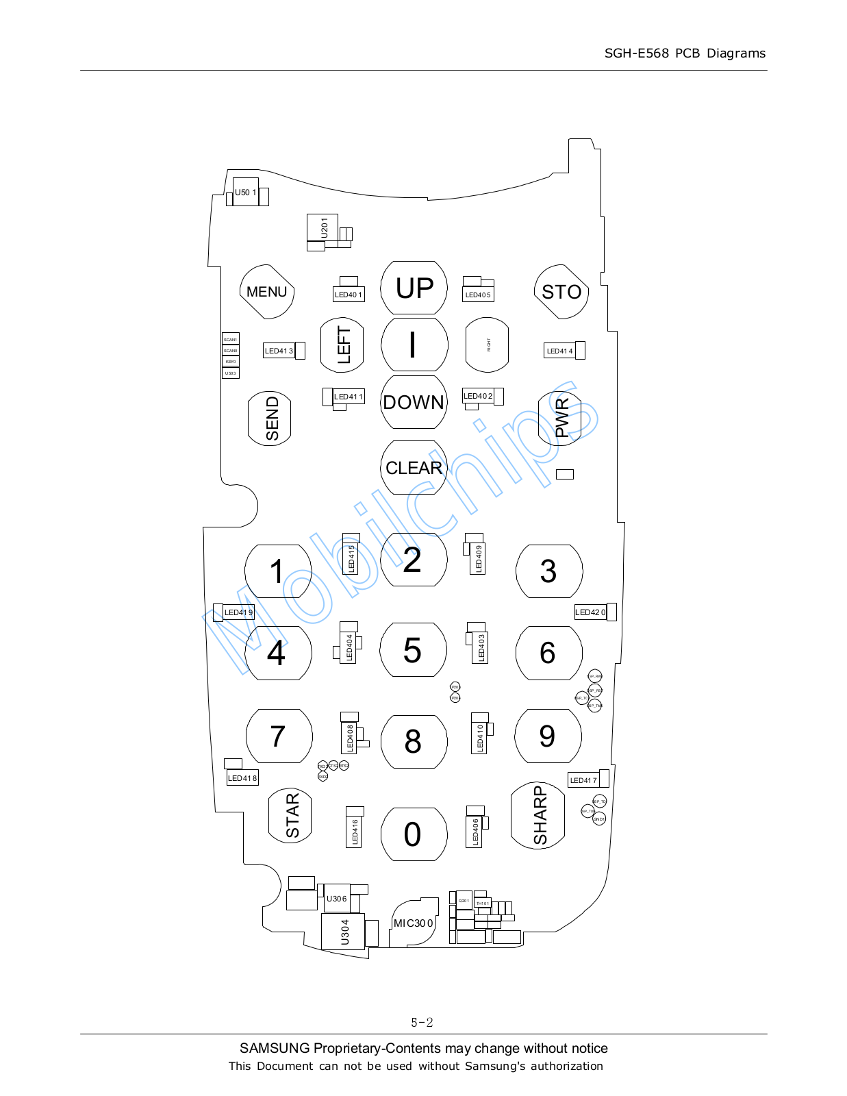
samsung SGH-X620 PCB Diagram
...
samsung PCB Diagram
Download
Specifications and Main Features
Frequently Asked Questions
User Manual
Download
Loading...
+
hidden pages
Unhide
You need points to download manuals.
1 point = 1 manual.
You can buy points or you can get point for every manual you upload.
Buy points
Upload your manuals
 Loading...