

Samsung SGH-X100 Schematics
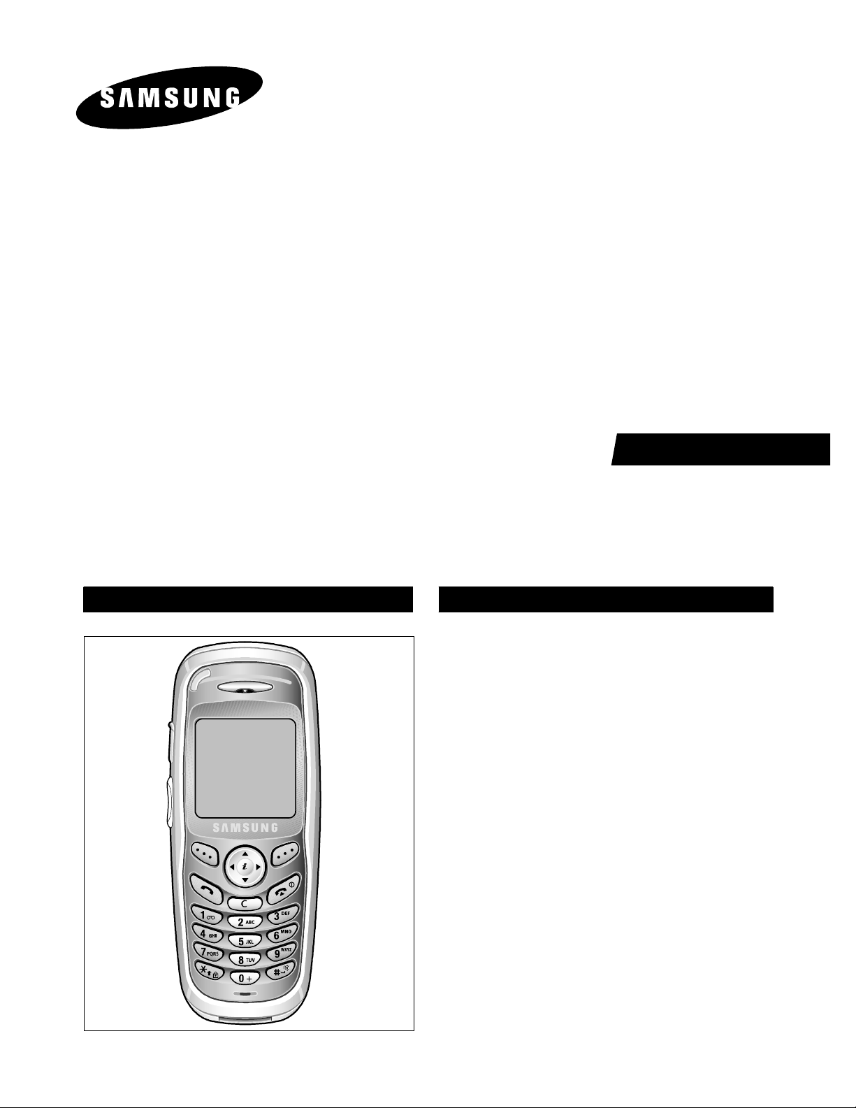
GSM TELEPHONE
SGH-X100
SERVICE
Manual
GSM TELEPHONE CONTENTS
1. Specification
2. Circuit Description
3. Exploded Views and Parts List
4. Electrical Parts List
5. Block Diagrams
6. PCB Diagrams
7. Flow Chart of Troubleshooting

ELECTRONICS
This Service Manual is a property of Samsung Electronics Co.,Ltd.
Any unauthorized use of Manual can be punished under applicable
International and/or domestic law.
ⓒ
Samsung Electronics Co.,Ltd. June. 2003
Printed in Korea.
Code No.: GH68-04326A
BASIC.
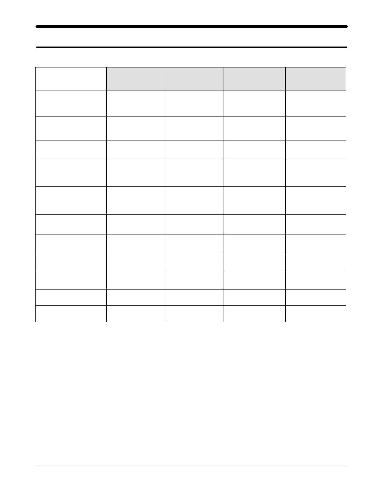
1. SGH-X100 Specification
1. GSM General Specification
GSM900
Phase 1
Freq. Band[MHz]
Uplink/Downlink
ARFCN range 1~124
Tx/Rx spacing 45MHz 45MHz 95MHz 80MHz
Mod. Bit rate/
Bit Period
Time Slot
Period/Frame Period
Modulation 0.3GMSK 0.3GMSK 0.3GMSK 0.3GMSK
MS Power 33dBm~13dBm 33dBm~5dBm 30dBm~0dBm 30dBm~0dBm
890~915
935~960
270.833kbps
3.692us
576.9us
4.615ms
EGSM 900
Phase 2
880~915
925~960
0~124 &
975~1023
270.833kbps
3.692us
576.9us
4.615ms
DCS1800
Phase 1
1710~1785
1805~1880
512~885 512~810
270.833kbps
3.692us
576.9us
4.615ms
PCS1900
1850~1910
1930~1990
270.833kbps
3.692us
576.9us
4.615ms
Power Class 5pcl ~ 15pcl 5pcl ~ 19pcl 0pcl ~ 15pcl 0pcl ~ 15pcl
Sensitivity -102dBm -102dBm -100dBm -100dBm
TDMA Mux 8 8 8 8
Cell Radius 35Km 35Km 2Km -
1-1
SAMSUNG Proprietary-Contents may change without notice
This Document can not be used without Samsung's authorization
SGH-V200 Specification
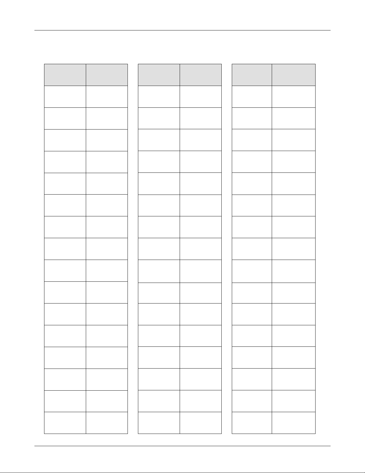
2. GSM TX power class
TX Power
control level
5 33±2 dBm
6 31±2 dBm
7 29±2 dBm
8 27±2 dBm
9 25±2 dBm
10 23±2 dBm
11 21±2 dBm
GSM900
TX Power
control level
0 30±3 dBm
1 28±3 dBm
2 26±3 dBm
3 24±3 dBm
4 22±3 dBm
5 20±3 dBm
6 18±3 dBm
DCS1800
TX Power
PCS1900
control level
0 30±3 dBm
1 28±3 dBm
2 26±3 dBm
3 24±3 dBm
4 22±3 dBm
5 20±3 dBm
6 18±3 dBm
12 19±2 dBm
13 17±2 dBm
14 15±2 dBm
15 13±2 dBm
16 11±3 dBm
17 9±3dBm
18 7±3 dBm
19 5±3 dBm
7 16±3 dBm
8 14±3 dBm
9 12±4 dBm
10 10±4 dBm
11 8±4dBm
12 6±4 dBm
13 4±4 dBm
14 2±5 dBm
7 16±3 dBm
8 14±3 dBm
9 12±4 dBm
10 10±4 dBm
11 8±4dBm
12 6±4 dBm
13 4±4 dBm
14 2±5 dBm
15 0±5 dBm
1-2
15 0±5 dBm
SAMSUNG Proprietary-Contents may change without notice
This Document can not be used without Samsung's authorization
2. SGH-X100 Circuit Description
1. SGH-
X108
RF Circuit Description
1) RX PART
1. ASM(U100)→Switching Tx, Rx path for GSM900, DCS1800 by logic controlling.
2. ASM Control Logic (U104, U106)→Truth Table
VC1 VC2
GSM Tx Mode H L
DCS Tx Mode L H
GSM Rx Mode L L
DCS Rx Mode L L
3. FILTER
To convert Electromagnetic Field Wave to Acoustic Wave and then pass the specific frequency band.
- GSM FILTER (F101)→For filtering the frequency band between 925 ~ 960 MHz
- DCS FILTER (F102)→For filtering the frequency band 1805 and 1880 MHz.
4. VC-TCXO (OSC101)
To generate the 26MHz reference clock to drive the logic and RF. After additional process, the reference clock applies to
the U103 Rx IQ demodulator and Tx IQ modulator. The oscillator for RX IQ demodulator and Tx modulator are
controlled by serial data to select channel and use fast lock mode for GPRS high class operation.
5. Transceiver (U103)
The receiver front-end converts the aerial RF signal from EGSM, DCS bands down to a low intermediate frequency (IF)
of 100 kHz. The first stages are symmetrical low noise amplifiers (LNAs). They are matched to 50 ohm. The LNAs are
followed by an I, Q down-mixer. It consists of two mixers in parallel but driven by quadrature out of phase LO signals.
The In phase (I) and Quadrature phase (Q) IF signals are low pass filtered to provide protection from high frequency
offset interferes. The low IF I and Q signals are then fed into the channel filter. The front-end low IF I and Q outputs
enter the integrated bandpass channel filter with provision for five 8 dB gain steps in front of the filter.
2-1
SAMSUNG Proprietary-Contents may change without notice
This Document can not be used without Samsung's authorization
SGH-X100 Circuit Description
2) TX PART
Baseband IQ signal fed into offset PLL, this function is included inside of U103 chip. OSC100 chip generates modulator
signal which power level is about 6.5dBm and fed into Power Amplifier(U101). The PA output power and power ramping
are well controlled by Auto Power Control circuit. We use offset PLL below
GSM -35dBc
DCS -35dBc
PCS -35dBc
GSM -66dBc
DCS -65dBc
PCS -66dBc
GSM -75dBc
DCS -68dBc
PCS -75dBc
Modulation Spectrum
200kHz offset
30 kHz bandwidth
400kHz offset
30 kHz bandwidth
600kHz ~ 1.8MHz offset
30 kHz bandwidth
2. Baseband Circuit description of SGH-X108
1. PCF50601
1.1 Power Management
Ten low-dropout regulators designed specifically for GSM applications power the terminal and help ensure optimal system
performance and long battery life. A programmable boost converter provides support for 1.8V, 3.0V, and 5.0V SIMs, while
a self-resetting, electronically fused switch supplies power to external accessories. Ancillary support functions, such as RTC
module and High Voltage Charge pump, Clock generator, aid in reducing both board area and system complexity.
I2C BUS serial interface provides access to control and configuration registers. This interface gives a microprocessor full
control of the PCF50601 and enables system designers to maximize both standby and talk times. Supervisory functions.
including a reset generator, an input voltage monitor, and a temperature sensor, support reliable system design. These
functions work together to ensure proper system behavior during start-up or in the event of a fault condition(low
microprocessor voltage, insufficient battery energy, or excessive die temperature).
1.2. Backlight Brightness Modulator
The Backlight Brightness Modulator (BBM) contains a programmable Pulse-width modulator (PWM) and FET to modulate
the intensity of a series of LED or to control a DC/DC converter that drives LCD backlight. This phone (SGH-X108) is
not use PWM, but use DC CONTROL (BACKLIGHT). So "BACKLIGHT" voltage is high value, backlight brigtness is
gloomy and "BACKLIGHT" voltage is low value, backlight is bright.
1.3. Clock Generato
The Clock Generator (CG) generates all clocks for internal and external usage. The 32768 Hz crystal oscillator provides an
accurate low clock frequency for the PCF50601 and other circuitry.
r
2-2
SAMSUNG Proprietary-Contents may change without notice
This Document can not be used without Samsung's authorization

2. SGH-X100 Circuit Description
2. Connector
2-1. LCD Connector
LCD is consisted of main LCD(color 65K STN LCD). Chip select signals in the U304, LCD_CS can enable LCD.
LCD_CS signal enables white LED of main LCD. This signal is from GPIO part of OM6357.
"RESET_2V8" signal initiates the Reset process of the LCD.
16-bit data lines(HD(0)~HD(15)) transfers data and commands to LCD through by pass capacitor. Data and commands use
"RS" signal. If this signal is high, Inputs to LCD are commands. If it is low, Inputs to LCD are data. The signal which
informs the input or output state to LCD, is required. But this system is not necessary this signal. So "L_WR" signal is
used to write data or commands to LCD. Power signali for LCD is "VDD3".
2-4. Key
This is consisted of key interface pins among OM6357, KBIO(0:7). These signals compose the matrix. Result of matrix
informs the key status to key interface in the OM6357. Power on/off key is seperated from the matrix. So power on/off
signal is connected with PCF50601 to enable PCF50601. ten key LEDs use the "VDD_KEY" supply voltage. "VDD_KEY"
signal enables LEDs with current control.
2-5. EMI ESD Filter
This system uses the EMI ESD filter, EMIF09 to protect noise from IF CONNECTOR part.
2-6 IF connetor
It is 18-pin connector. They are designed to use VBAT, V_EXT_CHARGE, TXD0, RXD0, RTS0, CTS0, JIG_REC,
CHARGER_OK, RXD1, TXD1, AUX_MIC, AUX_SPK and GND. They connected to power supply IC, microprocessor and
signal processor IC.
3. Battery Charge Management
a complete constant-current/constant-voltage linear charger for single cell lithium-ion batteries. If ta connected to phone,
"V_EXT_CHARGE" enable charger IC and supply current to battery. when fault condition caused, "CHG_ON" signal level
change low to high and charger IC stop charging process.
4. Audio
REC_P and REC_N from OM6357 are connected to the main receiver. AUXSP is connected to the Hands free kit.
MIC_P and MIC_N are connected to the main MIC. And AUX_MIC_P and AUX_MIC_N are connected to the Hands
free kit.
YMU762MA3 is a LSI for portable telephone that is capable of playing high quality music by utilizing FM sy nthesizer
and ADPCM decorder that are included in this device. As a synthesis, YMU762MA3 is equipped 32 voices with different
tones. Since the device is capable of simultaneously generating up to synchronous with the play of the FM synthesizer,
various sampled voices can be used as sound effects. Since the play data of YMU762MA3 are interpreted at anytime
through FIFO, the length of the data(playing period) is not limited, so the device can flexibly support application such as
incoming call melody music distribution service. The hardware sequencer built in this device allows playing of the
complex music without giving excessive load to the CPU of the portable telephones. Moreover, the registers of the FM
synthesizer can be operated directly for real time sound generation, allowing, for example, utilization of various sound
2-3
SAMSUNG Proprietary-Contents may change without notice
This Document can not be used without Samsung's authorization

SGH-X100 Circuit Description
effects when using the game software installed in the portable telephone. YMU762 includes a speaker amplifier with high
ripple removal rate whose maximum output is 550mW (SPVDD=3.6V). The device is also equipped with conventional
function including a vibartor and a circuit for controlling LEDs synchornous with music. For the headphone, it is provided
with a stereophonic output terminal. For the purpose of enabling YMU762MA3 to demonstrate its full capablities, Yamaha
purpose to use "SMAF:Synthetic music Mobile Application Format" as a data distribution format that is compatible with
multimedia. Since the SMAF takes a structure that sets importance on the synchronization between sound and images,
various contents can be written into it including incoming call melody with words that can be used for traning karaoke,
and commercial channel that combines texts, images and sounds, and others. The hardware sequencer of YMU762MA3
directly interprets and plays blocks relevant to systhesis (playing music and reproducing ADPCM with FM synthesizer) that
are included in data distributed in SMAF.
5. Memory
signals in the OM6357 enable two memories. They use only one volt supply voltage, VDD3 in the PCF50601. This
system uses Samsung's memory, KBB06A300M-T402. It is consisted of 128M bits flash NOR memory and 128M bits
flash NAND memory and 32M bits UtRAM. It has 16 bit data line, HD[0~15] which is connected to OM6357. It has 23
it address lines, HA[1~23]. CS_NAND and NCSRAM signals is chip select. Wrting process, HWR_N is low and it
enables writing process to flash memory and SRAM. During reading process, HRD_N is low and it enables reading
process to flash memory and SRAM. Each chip select signals in the OM6357 select memory among 2 flash memory and
UtRAM. Reading or writing procedure is processed after HWR_N or HRD_N is enabled. Memories use reset, which is
VDD3 delay from PCF50601. HA[22] signal enables lower byte of SRAM and HA[22] signal enables higher byte of
SRAM.
6. OM6357
OM6357 is consisted of ARM core and DSP core. It has 8x1Kword on-chip program/data RAM, 55 Kwords on-chip
program ROM in the DSP. It has 4K*32bits ROM and 2K*32bits RAM in the ARM core. DSP is consisted of KBS,
JTAG, EMI and UART. ARM core is consisted of EMI, PIC(Programmable Interrupt Controller), reset/power/clock unit,
DMA controller, TIC(Test Interface Controller), eripheral bridge, PPI, SSI(Synchronous Serial Interface), ACC(Asynchronous
communications controllers), timer, ADC, RTC(Real-Time Clock) and keyboard interface.
KBIO(0:7), address lines of DSP core and HD[0~15]. HA[1~23], address lines of ARM core and HD[0~15], data lines of
ARM core are connected to memory, YMU759. MV317S(Camera DSP Chip) controls the communication between ARM
core and DSP core.
CS_NAND, NCSRAM, NCSFLASH in the ARM core are connected to each memory. HWR_N and HRD_N control the
process of memory. External IRQ(Interrupt ReQuest) signals from each units, such as, PMU need the compatible process.
KBIO[0~7] receive the status from key and RXD0/TXD0/irDA_DOWN are used for the communications using IrDA and
data link cable(DEBUG_DTR/RTS/TXD/RXD/CTS/DSR).
It has JTAG control pins(TDI/TDO/TCK) for ARM core and DSP core. It recieves 13MHz clock in CKI pin from
external TCXO. ADC(Analog to Digital Convertor) part receives the status of temperature, battery type and battery voltage.
7. TCO-9141G(13MHz)
This system uses the 13MHz TCXO, TCO-9141G, Toyocom. AFC control signal form OM6357 controls frequency from
13MHz x-tal. It generates the clock frequency. This clock is connected to OM6357, YMU762.
2-4
SAMSUNG Proprietary-Contents may change without notice
This Document can not be used without Samsung's authorization
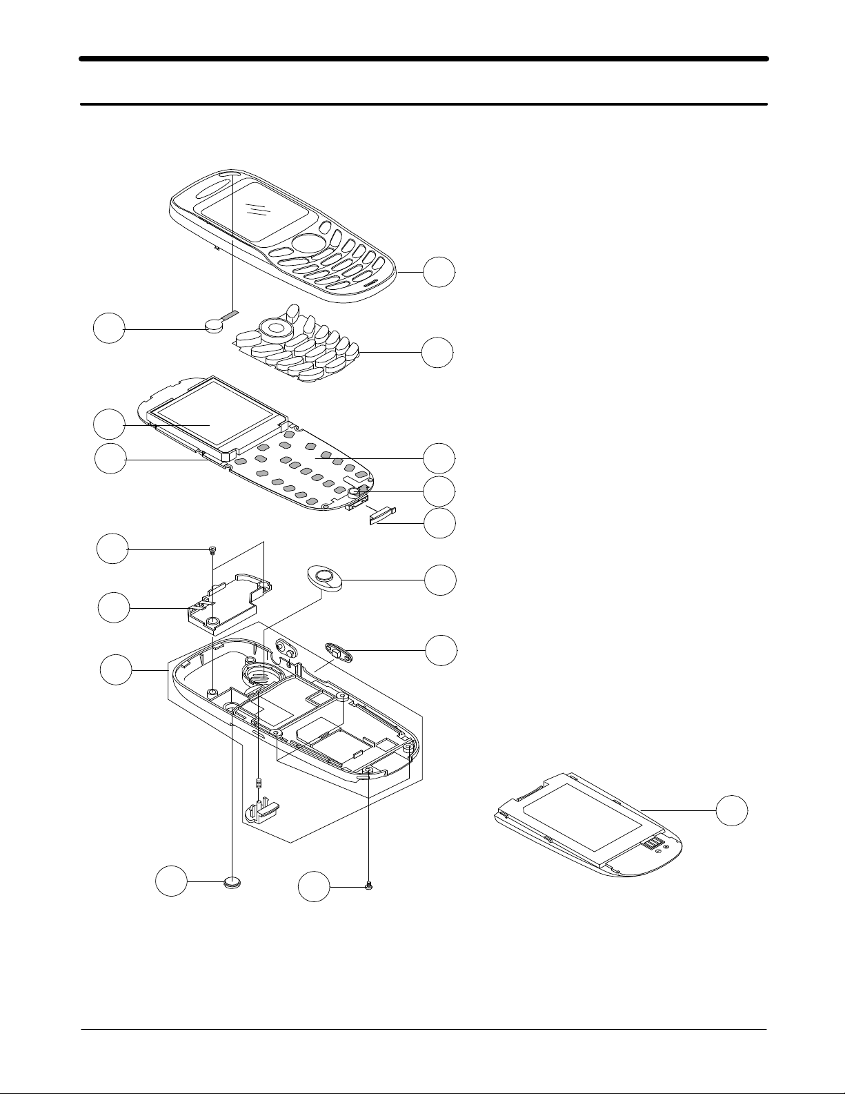
3. SGH-X100 Exploded View and its Parts list
1. Cellular phone Exploded View
1
3
2
9
10
11
12
13
4
5
6
7
8
16
14
15
3-1
SAMSUNG Proprietary-Contents may change without notice
This Document can not be used without Samsung's authorization
SGH- X100 Exploded view and its Part list
2. Cellular phone Parts list
NO DESCRIPTION SEC CODE REMARK
1 FRONT COVER GH75-03497A
2 KEYPAD GH75-03518A
3 AUDIO-RECEIVER 3009-001048
4 DOME SHEET GH59-00929A
5 MIC GH30-00044A
6 IF COVER GH73-02203A
7 MICRO SPEAKER 3001-001445
8 VOLKEY GH75-03728A
9 LCD GH07-00394A
10 MAIN PBA GH92-01558A
11 SCREW 6001-001654
12 INTENNA GH42-00308A
13 REAR COVER GH75-03496A
14 RF COVER GH72-09251A
15 SCREW 6001-001654
16 BATTERY GH43-00994A
3-2
SAMSUNG Proprietary-Contents may change without notice
This Document can not be used without Samsung's authorization
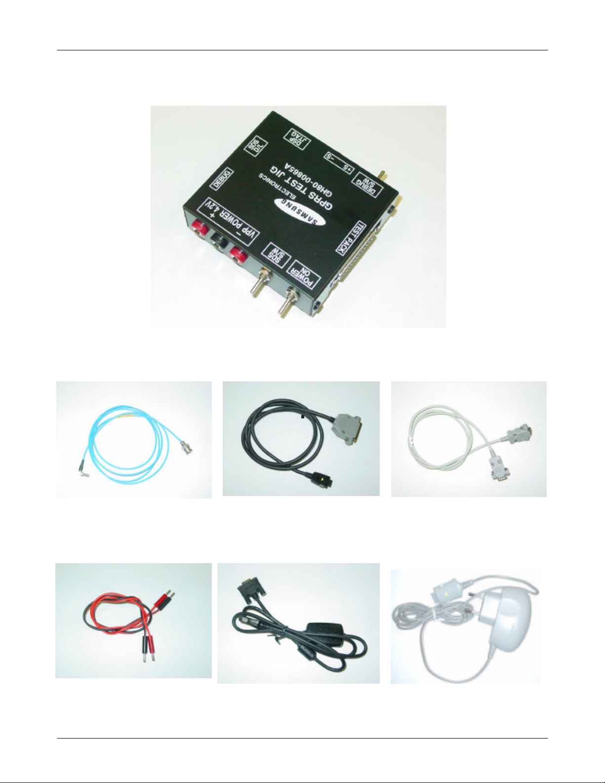
3. Test Jig (GH80-01909A)
SGH-X100 Exploded view and its Part list
3-1. RF Test Cable
(GH39-00140A)
3-2. Test Cable
(GH39-00217A)
3-4. Power Supply Cable 3-5. DATA CABLE
(GH39-00219A)
3-3. Serial Cable
3-6. TA
(GH44-00482G)
3-3
SAMSUNG Proprietary-Contents may change without notice
This Document can not be used without Samsung's authorization
4. SGH-X100 MAIN Electrical Parts List
SEC CODE Design LOC
0403-001446 ZD600
0406-001104 ZD201
0407-000115 D400
0504-001012 Q400
0504-001012 Q401
0504-001042 U104
0504-001042 U105
0504-001042 U106
0505-001423 U410
0506-000107 Q301,U405
0506-000107 U405
0601-001584 LED401
0601-001584 LED403
SEC CODE Design LOC
1203-002633 U307
1203-002764 U309
1204-001960 U301
1205-002257 U400
1205-002276 U200
1404-001256 TH200
1405-001082 V202
1405-001082 V204
1405-001082 V205
1405-001082 V207
1405-001082 V209
1405-001082 V210
1405-001082 V211
0601-001584 LED404
0601-001584 LED406
0601-001584 LED407
0601-001584 LED410
0601-001611 LED402
0601-001611 LED405
0601-001611 LED408
0601-001611 LED409
0801-002237 U300
0801-002529 U409
0801-002540 U211
0801-002540 U303
0801-002540 U304
1001-001183 U212
1405-001082 V212
1405-001082 V214
1405-001082 V215
1405-001082 V400
1405-001082 V401
1405-001082 V402
1405-001082 V403
1405-001082 V404
2007-000138 R132
2007-000138 R411
2007-000138 R412
2007-000140 R123
2007-000140 R124
2007-000140 R324
1109-001243 U305
1201-001954 U101
1202-001036 U203
SAMSUNG Proprietary-Contents may change without notice
This Document can not be used without Samsung's authorization
2007-000141 R105
2007-000141 R225
2007-000141 R226
4-1
SGH-X100 Electrical Parts List
SEC CODE Design LOC
2007-000143 R135
2007-000143 R136
2007-000143 R137
2007-000143 R138
2007-000143 R362
2007-000144 R115
2007-000147 R116
2007-000148 R126
2007-000148 R202
2007-000148 R204
2007-000148 R205
2007-000148 R210
2007-000148 R227
SEC CODE Design LOC
2007-000162 R361
2007-000164 R339
2007-000167 U730
2007-000171 R100
2007-000171 R109
2007-000171 R117
2007-000171 R107
2007-000171 R119
2007-000171 R121
2007-000171 R139
2007-000171 R213
2007-000171 R214
2007-000171 R228
2007-000148 R342
2007-000148 R410
2007-000148 U732
2007-000157 R321
2007-000162 R101
2007-000162 R102
2007-000162 R103
2007-000162 R203
2007-000162 R211
2007-000162 R212
2007-000162 R229
2007-000162 R237
2007-000162 R270
2007-000162 R300
2007-000171 R230
2007-000171 R231
2007-000171 R274
2007-000171 R307
2007-000171 R320
2007-000171 R414
2007-000172 R120
2007-000172 R131
2007-000174 R129
2007-000242 R200
2007-000242 R206
2007-000566 R125
2007-000566 R127
2007-000566 R337
2007-000162 R323
2007-000162 R350
2007-000162 R360
SAMSUNG Proprietary-Contents may change without notice
This Document can not be used without Samsung's authorization
2007-001288 R108
2007-001288 R112
2007-001301 R401
4-2
 Loading...